Document Outline
- COVER
- FEATURES
- APPLICATION FIELDS
- ORDERING INFORMATION
- QUALITY GRADE
- DIFFERENCES AMONG uPD78P324, 78P324(A), 78P324(A1), AND 78P324(A2)
- PIN CONFIGURATION (Top View)
- INTERNAL BLOCK DIAGRAM
- 1. LIST OF PIN FUNCTIONS
- 1.1 NORMAL OPERATION MODE
- 1.2 PROM PROGRAMMING MODE (RESET# = H, AVDD = L)
- 1.3 PIN I/O CIRCUIT AND UNUSED-PIN PROCESSING
- 2. DIFFERENCES BETWEEN uPD78P324 AND uPD78324
- 3. PROM PROGRAMMING
- 3.1 OPERATION MODE
- 3.2 PROCEDURE FOR PROM WRITE
- 3.3 PROCEDURE FOR PROM
- 4. ERASURE CHARACTERISTICS (uPD78P324KC/KD ONLY)
- 5. ERASURE WINDOW SEAL (uPD78P324KC/KD ONLY)
- 6. ONE-TIME PROM PRODUCT SCREENING
- 7. ELECTRICAL SPECIFICATIONS
- 8. PACKAGE DRAWINGS
- 9. RECOMMENDED SOLDERING CONDITIONS
- APPENDIX A. CONVERSION SOCKET PACKAGE DRAWING AND RECOMMENDED SUBSTRATE INSTALLATION PATTERN
- APPENDIX B. TOOLS
- B.1 DEVELOPMENT TOOLS
- B.2 EVALUATION TOOLS
- B.3 EMBEDDED SOFTWARE

µ
PD78P324, 78P324(A)
MOS INTEGRATED CIRCUIT
The information in this document is subject to change without notice.
16-/8-Bit Single-Chip Microcomputers
©
1991, 1995
DATA SHEET
The
µ
PD78P324 is a product in which the
µ
PD78324's internal mask ROM is replaced by a one-time PROM
or EPROM. The one-time PROM product, which enables writing only once, is effective for multiple-device
small production of sets or early start of mass-production. The EPROM product, which enables program
writing, deletion, and rewriting, is the most suitable for system evaluation.
The
µ
PD78P324(A) is more reliable than the
µ
PD78P324. The
µ
PD78P324(A) is a product resulting from
the
µ
PD78324(A) whose internal mask ROM is replaced by a one-time PROM.
For details of functions, please refer to the following User's Manual. Reading this manual is indispensable
especially for designing work.
µ
PD78322 User's Manual: IEU-1248
FEATURES
q
µ
PD78324 compatible
∑ For mass-production, this can be replaced by the
µ
PD78324 incorporated in the mask ROM.
q Minimum instruction run time: 250 ns (with the external clock operating at 16 MHz):
µ
PD78P324 & 78P324(A)
320 ns (with the external clock operating at 12.5 MHz):
µ
PD78P324(A1) &
78P324(A2)
q Internal PROM: 32768 x 8 bits
∑ Writing enabled only once (windowless one-time PROM product)
∑ Elimination by ultraviolet light and electrical rewriting enabled (EPROM product with window):
µ
PD78P324
only
q ECC circuit incorporated
∑ High internal PROM content reliablility possible
q PROM programming characteristic:
µ
PD27C1001A compatible
q QTOP
TM
microcomputer compatible
Remark
A QTOP microcomputer is a single-chip microcomputer with one-time PROM for which program
writing, marking, screening, and verifying is completely supported by NEC.
APPLICATION FIELDS
q
µ
PD78P324: Fields dealing with motor control equipment.
q
µ
PD78P324(A), 78P324(A1), and 78P324(A2): Automotive and transportation equipments, etc.
This document describes the
µ
PD78P324, 78P324(A),
µ
PD78P324(A1), and
µ
PD78P324(A2) as well. However,
unless there are particular differences, the
µ
PD78P324 is described as a representative product. PROM is
the representative term used for the part common to both the one-time PROM product and the EPROM
product.
Document No. IC-2857
(O. D. No. IC-8315)
Date Published January 1995 P
Printed in Japan

µ
PD78P324, 78P324(A)
2
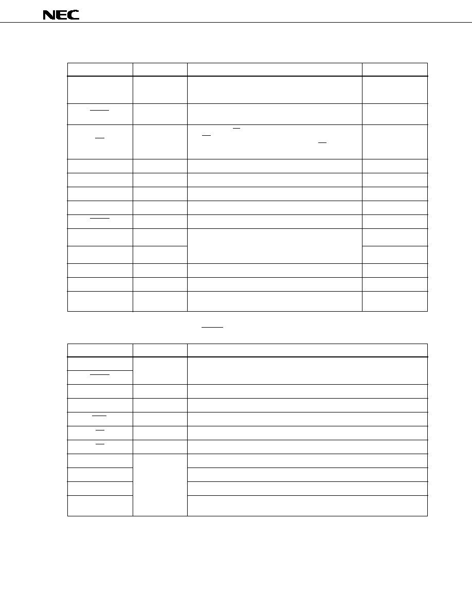
ORDERING INFORMATION
Part No.
Package
Internal ROM
Operating Temperature (T
A
)
µ
PD78P324GJ-5BJ
74-pin plastic QFP(20 x 20 mm)
One-time PROM
≠10 to +70
∞
C
µ
PD78P324LP
68-pin plastic QFJ(
s
s
950 mil)
One-time PROM
≠10 to +70
∞
C
µ
PD78P324KC
68-pin ceramic WQFN
EPROM
≠10 to +70
∞
C
µ
PD78P324KD
74-pin ceramic WQFN
EPROM
≠10 to +70
∞
C
µ
PD78P324GJ(A)-5BJ
74-pin plastic QFP(20 x 20 mm)
One-time PROM
≠40 to +85
∞
C
µ
PD78P324GJ(A1)-5BJ
74-pin plastic QFP(20 x 20 mm)
One-time PROM
≠40 to +110
∞
C
µ
PD78P324GJ(A2)-5BJ
74-pin plastic QFP(20 x 20 mm)
One-time PROM
≠40 to +125
∞
C
µ
PD78P324LP(A)
68-pin plastic QFJ(
s
s
950 mil)
One-time PROM
≠40 to +85
∞
C
µ
PD78P324LP(A1)
68-pin plastic QFJ(
s
s
950 mil)
One-time PROM
≠40 to +110
∞
C
µ
PD78P324LP(A2)
68-pin plastic QFJ(
s
s
950 mil)
One-time PROM
≠40 to +125
∞
C
QUALITY GRADE
Part No.
Quality Grade
µ
PD78P324GJ-5BJ
Standard
µ
PD78P324LP
Standard
µ
PD78P324KC
Standard
µ
PD78P324KD
Standard
µ
PD78P324GJ(A)-5BJ
Special
µ
PD78P324GJ(A1)-5BJ
Special
µ
PD78P324GJ(A2)-5BJ
Special
µ
PD78P324LP(A)
Special
µ
PD78P324LP(A1)
Special
µ
PD78P324LP(A2)
Special
Please refer to "Quality grade on NEC Semiconductor Devices" (Document number IEI-1209) published by
NEC Corporation to know the specification of quality grade on the devices and its recommended applications.

µ
PD78P324, 78P324(A)
3
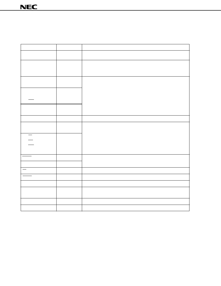
DIFFERENCES AMONG
µ
PD78P324, 78P324(A), 78P324(A1), AND 78P324(A2)
Product Name
Parameter
Quality grade
Operating ambient tempera-
ture (T
A
)
Operating frequency
Minimum instruction
execution time
Permissible pin injection
current characteristics on
overvoltage application
DC characteristics
AC characteristics
A/D converter characteristics
One-time PROM product
EPROM product
µ
PD78P324
µ
PD78P324(A)
µ
PD78P324(A1)
µ
PD78P324(A2)
Standard
Special
≠10 to +70
∞
C
≠40 to +85
∞
C
≠40 to +110
∞
C
≠40 to +125
∞
C
8 to 16 MHz
8 to 12.5 MHz
250 ns (when operated at 16 MHz)
320 ns (when operated at 12.5 MHz)
None
Provided
Differ in the analog pin input leak current, the V
DD
supply current, and the data retention
current.
Differ in the bus timing.
Differ in the analog input voltage and the A/D converter data retention current.
Provided
Provided
None
µ
PD78P324, 78P324(A)
4
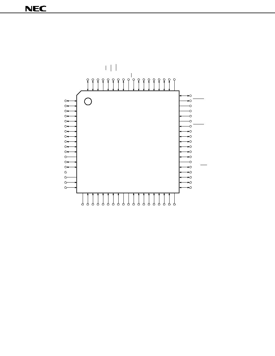
PIN CONFIGURATION (Top View)
(1) Normal operation mode
(a) 74-pin plastic QFP(20 x 20 mm); 74-pin ceramic WQFN
P43/AD3
P44/AD4
P45/AD5
P46/AD6
P47/AD7
P50/A8
P51/A9
P52/A10
P53/A11
P54/A12
P55/A13
NC
P56/A14
P57/A15
V
DD
AV
SS
P70/AN0
P71/AN1
1
2
3
4
5
6
7
8
9
10
11
12
13
14
15
16
17
18
55
54
53
52
51
50
49
48
47
46
45
44
43
42
41
40
39
38
19 20 21 22 23 24 25 26 27 28 29 30 31 32 33 34 35 36 37
74 73 72 71 70 69 68 67 66 65 64 63 62 61 60 59 58
P 0/RTP0
WDTO
V
SS
NC
X1
X2
RESET
P85/TO11
P84/TO10
P83/TO03
P82/TO02
P81/TO01
P80/TO00
NC
P34/SCK
P33/SI/SB1
P32/SO/SB0
P31/R
X
D
P30/T
X
D
P42/AD2
P41/AD1
P40/AD0
ASTB
P90/RD
P91/WR
P92/TAS
P93/TMD
V
SS
EA
P07/RTP7
P06/RTP6
P05/RTP5
P04/RTP4
P03/RTP3
P02/RTP2
P01/RTP1
NC
NC
P72/AN2
P73/AN3
P74/AN4
P75/AN5
P76/AN6
P77/AN7
AV
REF
AV
DD
V
DD
P20/NMI
P21/INTP0
P22/INTP1
P23/INTP2
P24/INTP3
P25/INTP4
P26/INTP5
P27/INTP6
NC
PD78P324GJ-5BJ
PD78P324KD
PD78P324GJ(A)-5BJ
PD78P324GJ(A1)-5BJ
PD78P324GJ(A2)-5BJ
57
56
µ
µ
µ
µ
µ
ÿ
Caution
As a measure against noise, please connect the NC pin to V
SS
. (It is also possible to leave this pin
unconnected.)
Remark
Pin-compatible with
µ
PD78324GJ.
µ
PD78P324, 78P324(A)
5
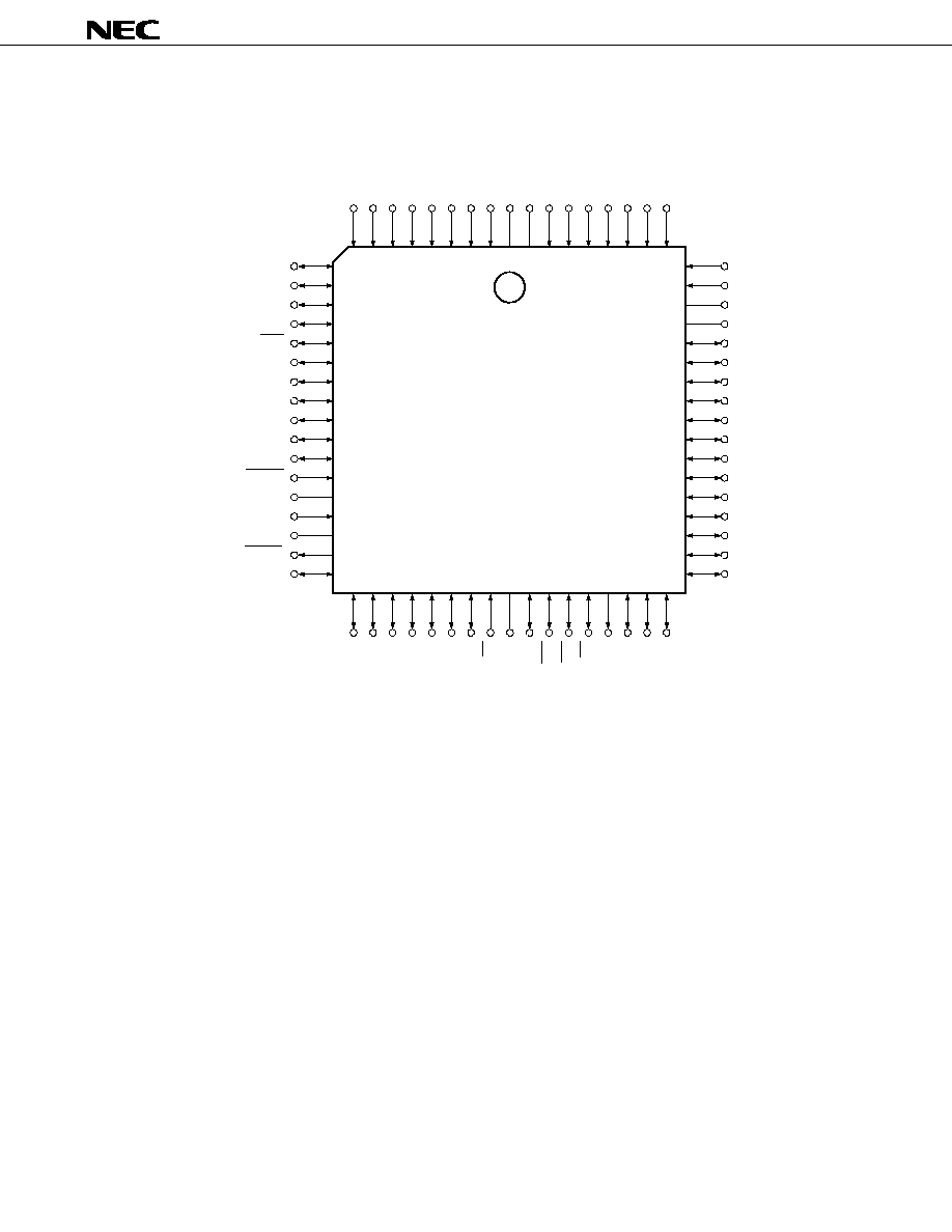
(b) 68-pin plastic QFJ(
s
s
950 mil); 68-pin ceramic WQFN
10
11
12
13
14
15
16
17
18
19
20
21
22
23
24
25
26
60
59
58
57
56
55
54
53
52
51
50
49
48
47
46
45
44
P71/AN1
P70/AN0
AV
SS
V
DD
P57/A15
P56/A14
P55/A13
P54/A12
P53/A11
P52/A10
P51/A9
P50/A8
P47/AD7
P46/AD6
P45/AD5
P44/AD4
P43/AD3
PD78P324LP
PD78P324KC
PD78P324LP(A)
PD78P324LP(A1)
PD78P324LP(A2)
P30/T
X
D
P31/R
X
D
P32/SO/SB0
P33/SI/SB1
P34/SCK
P80/TO00
P81/TO01
P82/TO02
P83/TO03
P84/TO10
P85/TO11
RESET
X2
X1
V
SS
WDTO
RTP /P00
9
8
7
6
5
4
3
2
1 68 67 66 65 64 63 62 61
27 28 29 30 31 32 33 34 35 36 37 38 39 40 41 42 43
P01/RTP1
P02/RTP2
P03/RTP3
P04/RTP4
P05/RTP5
P06/RTP6
P07/RTP7
EA
V
SS
P93/TMD
P92/TAS
P91/WR
P90/RD
ASTB
P40/AD0
P41/AD1
P42/AD2
P27/INTP6/T1
P26/INTP5
P25/INTP4
P24/INTP3
P23/INTP2
P22/INTP1
P21/INTP0
P20/NMI
V
DD
AV
DD
AV
REF
P77/AN7
P76/AN6
P75/AN5
P74/AN4
P73/AN3
P72/AN2
µ
µ
µ
µ
µ
0
Remark
Pin-compatible with
µ
PD78324LP.

µ
PD78P324, 78P324(A)
6
P00-P07
: Port0
P20-P27
: Port2
P30-P34
: Port3
P40-P47
: Port4
P50-P57
: Port5
P70-P77
: Port7
P80-P85
: Port8
P90-P93
: Port9
NMI
: Nonmakable Interrupt
INTP0-INTP6
: Interrupt from Peripherals
RTP0-RTP7
: Realtime Port
TI
: Timer Input
T
X
D
: Transmit Data
R
X
D
: Receive Data
SB0/SO
: Serial Bus/Serial Output
SB1/SI
: Serial Bus/Serial Input
SCK
: Serial Clock
TO00-TO03
:
TO10, TO11
:
RESET
: Reset
X1, X2
: Crystal
WDTO
: Watchdog Timer Output
EA
: External Access
TMD
: Turbo Mode
TAS
: Turbo Access Strobe
WR
: Write Strobe
RD
: Read Strobe
ASTB
: Address Strobe
AD0-AD7
: Address/Data Bus
A8-A15
: Address Bus
AN0-AN7
: Analog Input
AV
REF
: Analog Reference Voltage
AV
SS
: Analog V
SS
AV
DD
: Analog V
DD
V
DD
: Power Supply
V
SS
: Ground
NC
: Non-connection
Timer Output
µ
PD78P324, 78P324(A)
7
(2) PROM programming mode (RESET = H, AV
DD
= L)
(a) 74-pin plastic QFP (20 x 20 mm); 74-pin ceramic WQFN
Cautions
1. Codes marked by brackets refer to processing by pins unused in PROM programming mode.
L
: Connect to V
SS
individually via a resistor.
G
: Connect to V
SS
.
Open
: Do not connect anything.
2. As a measure against noise, please connect the NC pin to V
SS
. (It is also possible to leave this pin
unconnected.)
D2
D1
D0
(Open)
V
SS
V
PP
A7
A6
A5
A4
A3
A2
A1
NC
(L)
74 73 72 71 70 69 68 67 66 65 64 63 62 61 60 59 58 57
A0
(Open)
V
SS
NC
(G)
(Open)
RESET
A14
A13
A12
A11
A10
A8
NC
A16
A15
PGM
CE
OE
56
55
54
53
52
51
50
49
48
47
46
45
44
43
42
41
40
39
38
PD78P324GJ-5BJ
PD78P324KD
PD78P324GJ(A)-5BJ
PD78P324GJ(A1)-5BJ
PD78P324GJ(A2)-5BJ
19 20 21 22 23 24 25 26 27 28 29 30 31 32 33 34 35 36 37
NC
AV
DD
V
DD
A9
NC
(L)
(G)
(G)
1
2
3
4
5
6
7
8
9
10
11
12
13
14
15
16
17
18
D3
D4
D5
D6
D7
NC
V
DD
(G)
(L)
(L)
µ
µ
µ
µ
µ

µ
PD78P324, 78P324(A)
8
(b) 68-pin plastic QFJ(
s
s
950 mil); 68-pin ceramic WQFN
Caution
Codes marked by brackets refer to processing by pins unused in PROM programming mode.
L
: Connect to V
SS
individually via a resistor.
G
: Connect to V
SS
.
Open
: Do not connect anything.
A0-A16
: Address Bus
D0-D7
: Data Bus
CE
: Chip Enable
OE
: Output Enable
PGM
: Programming Mode
RESET
:
AV
DD
:
V
PP
: Programming Power Supply
NC
: Non-connection
Programming Mode Set
A9
V
DD
AV
DD
(L)
(G)
(G)
9
8
7
6
5
4
3
2
1 68 67 66 65 64 63 62 61
PD78P324LP
PD78P324KC
PD78P324LP(A)
PD78P324LP(A1)
PD78P324LP(A2)
27 28 29 30 31 32 33 34 35 36 37 38 39 40 41 42 43
A1
A2
A3
A4
A5
A6
A7
V
PP
V
SS
(Open)
D0
D1
D2
(L)
60
59
58
57
56
55
54
53
52
51
50
49
48
47
46
45
44
V
DD
D7
D6
D5
D4
D3
(G)
(L)
10
11
12
13
14
15
16
17
18
19
20
21
22
23
24
25
26
OE
CE
PGM
A15
A16
A8
A10
A11
A12
A13
A14
RESET
(Open)
(G)
V
SS
(Open)
A0
µ
µ
µ
µ
µ
µ
PD78P324, 78P324(A)
9
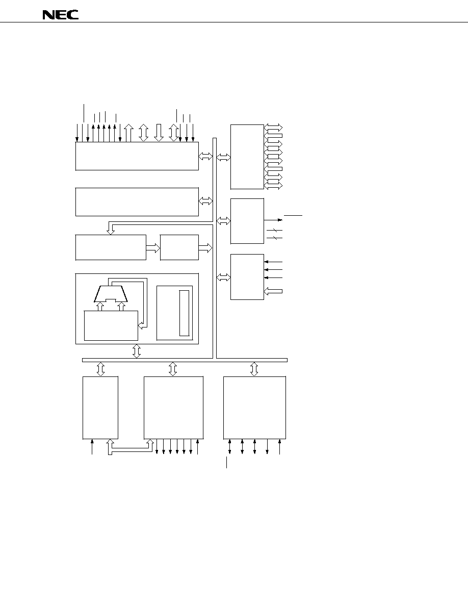
INTERNAL BLOCK DIAGRAM
Remark
*: When in PROM programming mode
(P20) NMI
INTP0-INTP5
(P21-P26)
(P80) TO00
(P81) TO01
(P82) TO02
(P83) TO03
(P84) TO10
(P85) TO11
(P27) T1/INTP6
(P34) SCK
(P32) SO/SB0
(P33) SI/SB1
(P30) T
X
D
(P31) R
X
D
PROGRAMMABLE
INTERRUPT
CONTROLLER
TINER/COUNTER UNIT
(REAL TIME PULSE UNIT)
SERIAL INTERFFACE
(SBI)
(UART)
EXU
PROM
Peripheral RAM
BCU
Main RAM
ALU
ECC
32K
bytes
768
bytes
SYSTEM
CONTROL
&
BUS
CONTROL
&
PREFETCH
CONTROL
PORT
WDT
GENERAL
REGISTERS
128 bytes
&
DATA
MEMORY
128 bytes
MICRO
SEQUENCE
CONTROL
MICRO ROM
A/D CONVERTER
(10 BITS)
X1
X2
RESET
ASTB
RD
WR
TAS
TMD
EA/V
PP
*
A8-A15 (P50-P57)
AD0-AD7 (P40-P47)
A0-A16*
D0-D7*
PGM*
CE*
OE*
P00-P07 (REALTIME PORT)
P20-P27
P30-P34
P40-P47
P50-P57
P70-P77
P80-P85
P90-P93
WDTO
V
DD
V
SS
2
2
AV
REF
AV
SS
AV
DD
AN0-AN7
(P70-P77)

µ
PD78P324, 78P324(A)
10
TABLE OF CONTENTS
1.
LIST OF PIN FUNCTIONS ...........................................................................................................
11
1.1
NORMAL OPERATION MODE ...........................................................................................................
11
1.2
PROM PROGRAMMING MODE (RESET = H, AV
DD
= L) .................................................................
13
1.3
PIN I/O CIRCUIT AND UNUSED-PIN PROCESSING .......................................................................
14
2.
DIFFERENCE BETWEEN
µ
PD78P324 AND
µ
PD78324 ..............................................................
16
3.
PROM PROGRAMMING ..............................................................................................................
17
3.1
OPERATION MODE ............................................................................................................................
18
3.2
PROCEDURE FOR PROM WRITE ......................................................................................................
19
3.3
PROCEDURE FOR PROM READ ........................................................................................................
21
4.
ERASURE CHARACTERISTICS (
µ
PD78P324KC/KD ONLY) .....................................................
22
5.
ERASURE WINDOW SEAL (
µ
PD78P324KC/KD ONLY) ...........................................................
22
6.
ONE-TIME PROM PRODUCT SCREENING ................................................................................
22
7.
ELECTRICAL SPECIFICATIONS ..................................................................................................
23
8.
PACKAGE DRAWINGS ................................................................................................................
65
9.
RECOMMENDED SOLDERING CONDITIONS ...........................................................................
69
APPENDIX A. CONVERSION SOCKET PACKAGE DRAWING AND
RECOMMENDED SUBSTRATE INSTALLATION PATTERN ..................................
71
APPENDIX B. TOOLS .........................................................................................................................
73
B.1
DEVELOPMENT TOOLS .....................................................................................................................
73
B.2
EVALUATION TOOLS ........................................................................................................................
77
B.3
EMBEDDED SOFTWARE ....................................................................................................................
77

µ
PD78P324, 78P324(A)
11
1.
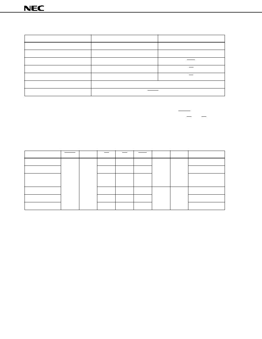
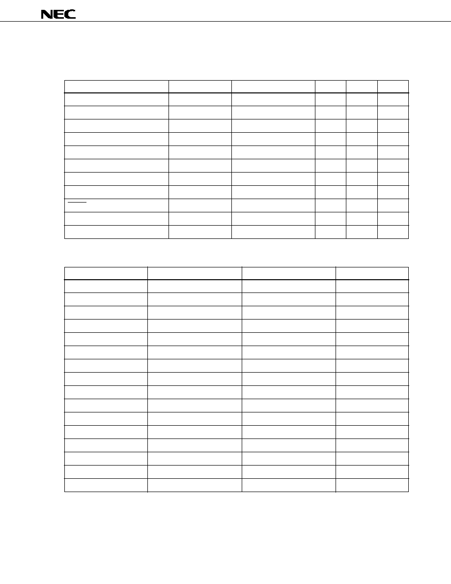
LIST OF PIN FUNCTIONS
1.1
NORMAL OPERATION MODE
(1) Port pins
Pin Name
P00-P07
P20
P21
P22
P23
P24
P25
P26
P27
P30
P31
P32
P33
P34
P40-P47
P50-P57
P70-P77
P80
P81
P82
P83
P84
P85
P90
P91
P92
P93
Function
Port 0.
8-bit I/O port.
I/O specifiable per bit.
(Operable as a real-time output port as well.)
Port 2.
8-bit input-only port.
Port 3.
5-bit I/O port.
I/O specifiable per bit.
Port 4.
8-bit I/O port.
I/O specifiable in units of eight bits.
Port 5.
8-bit I/O port.
I/O specifiable per bit.
Port 7.
8-bit input-only port.
Port 8.
6-bit I/O port.
I/O specifiable per bit.
Port 9.
4-bit I/O port.
I/O specifiable per bit.
Shared Pin Name
RTP0-RTP7
NMI
INTP0
INTP1
INTP2
INTP3
INTP4
INTP5
INTP6/TI
T
X
D
R
X
D
SO/SB0
SI/SB1
SCK
AD0-AD7
A8-A15
AN0-AN7
TO00
TO01
TO02
TO03
TO10
TO11
RD
WR
TAS
TMD
I/O
I/O
Input
I/O
I/O
I/O
Input
I/O
I/O

µ
PD78P324, 78P324(A)
12
(2) Pins other than ports (1/2)
I/O
Output
Input
Input
Input
Input
Output
Input
Output
I/O
I/O
I/O
Output
Output
Output
Output
Function
Real-time output port performing pulse outputs synchro-
nously with the trigger symbols from the real-time pulse
unit (RPU).
External interrupt request input of edge detection.
A valid edge can be selected by the external interrupt
mode register.
Non-maskable interrupt request input of edge detection.
A valid edge can be selected by the external interrupt
mode register.
External counter clock input to Timer 1 (TM1).
Serial data input of the asynchronous serial interface
(UART).
Serial data output of the asynchronous serial interface
(UART).
Serial data input in three-wire mode of the clock synchro-
nous serial interface.
Serial data input in three-wire mode of the clock synchro-
nous serial interface.
Serial data output in three-wire mode of the clock
synchronous serial interface.
Serial clock I/O of the clock synchronous serial interface.
Address data bus for accessing external memory.
Address bus for accessing external memory.
Read signal output to external memory.
Write signal output to external memory.
Control signal output for accessing the turbo access
manager (
µ
PD71P301)
Note
.
Output from the real-time pulse unit.
Shared Pin Name
P00-P07
P21
P22
P23
P24
P25
P26
P27/TI
P20
P27/INTP6
P31
P30
P33/SB1
P32/SB0
P32/SO
P33/SI
P34
P40-P47
P50-P57
P90
P91
P92
P93
P80
P81
P82
P83
P84
P85
Pin Name
RTP0-RTP7
INTP0
INTP1
INTP2
INTP3
INTP4
INTP5
INTP6
NMI
TI
R
X
D
T
X
D
SI
SO
SB0
SB1
SCK
AD0-AD7
A8-A15
RD
WR
TAS
TMD
TO00
TO01
TO02
TO03
TO10
TO11
Note
The turbo access manager (
µ
PD71P301) is a maintenance product.
µ
PD78P324, 78P324(A)
13
(2) Pins other than ports (2/2)
I/O
Output
Output
Input
Input
Input
--
--
Input
Input
--
--
--
--
Function
Access to external memory. Timing signal output for
externally latching the lower address which is output
from the AD0-AD7 pin.
Output of the signal which indicates that the watchdog
timer generated a non-maskable interrupt.
Normally, the EA pin is connected to V
DD
. By connecting
the EA pin to Vss, the system is placed in ROM-less mode
to access external memory. The level of the EA pin
cannot be switched over during operation.
Analog input to the A/D converter
Reference voltage input of the A/D converter.
Analog power of the A/D converter.
Ground of the A/D converter.
Input of the system reset.
Connection of the crystal oscillator for system clock
generation. When clocks are supplied externally, they are
input to the X1 pin and their reverse signals are input to
the X2 pin. (The X2 pin can also be left unconnected.)
Positive power voltage.
Ground.
Internally unconnected. Please connect this to Vss. (It can
also be left unconnected.)
Shared Pin Name
--
--
--
P70-P77
--
--
--
--
--
--
--
--
--
Pin Name
ASTB
WDTO
EA
AN0-AN7
AV
REF
AV
DD
AV
SS
RESET
X1
X2
V
DD
V
SS
NC
1.2
PROM PROGRAMMING MODE (RESET = H, AV
DD
= L)
I/O
Input
Input
I/O
Input
Input
Input
--
Function
PROM programming mode setting
Address bus
Data bus
Program input
PROM enable input
Read strobe to PROM
Write power
Positive power voltage
Ground
Internally unconnected. Please connect this to V
SS
. (It can also be left uncon-
nected.)
Pin Name
AV
DD
RESET
A0-A16
D0-D7
PGM
CE
OE
V
PP
V
DD
V
SS
NC
µ
PD78P324, 78P324(A)
14
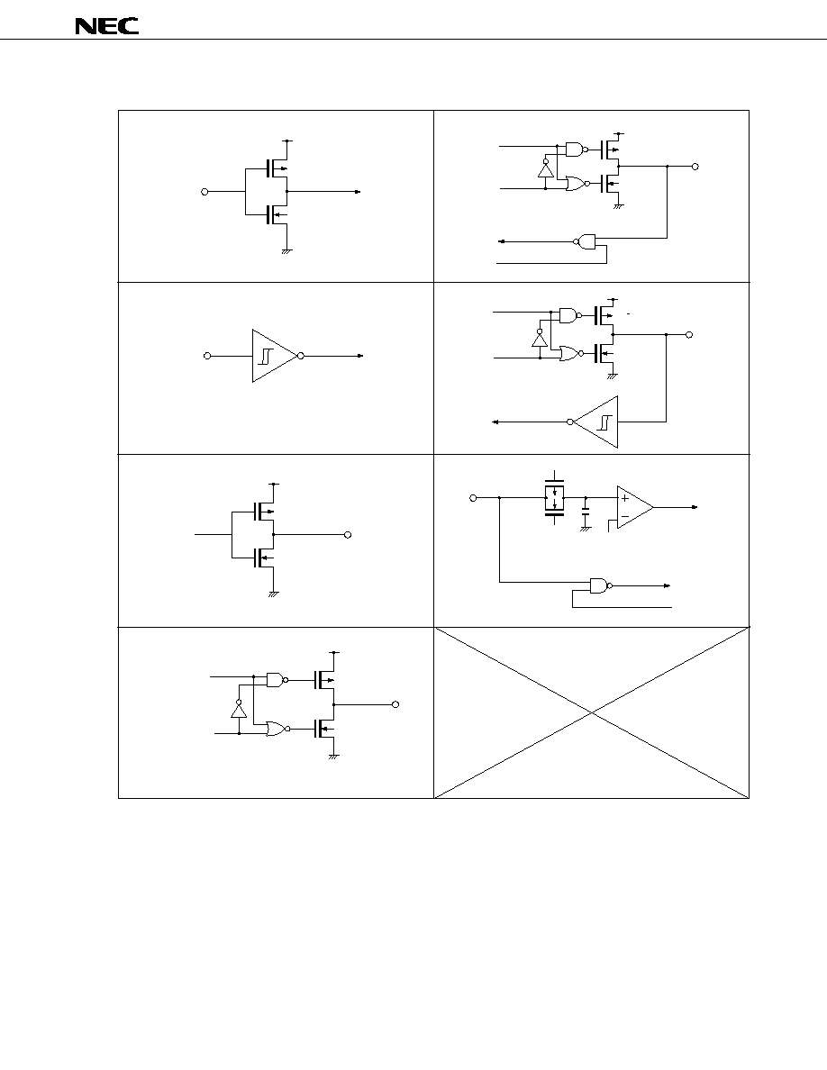
1.3
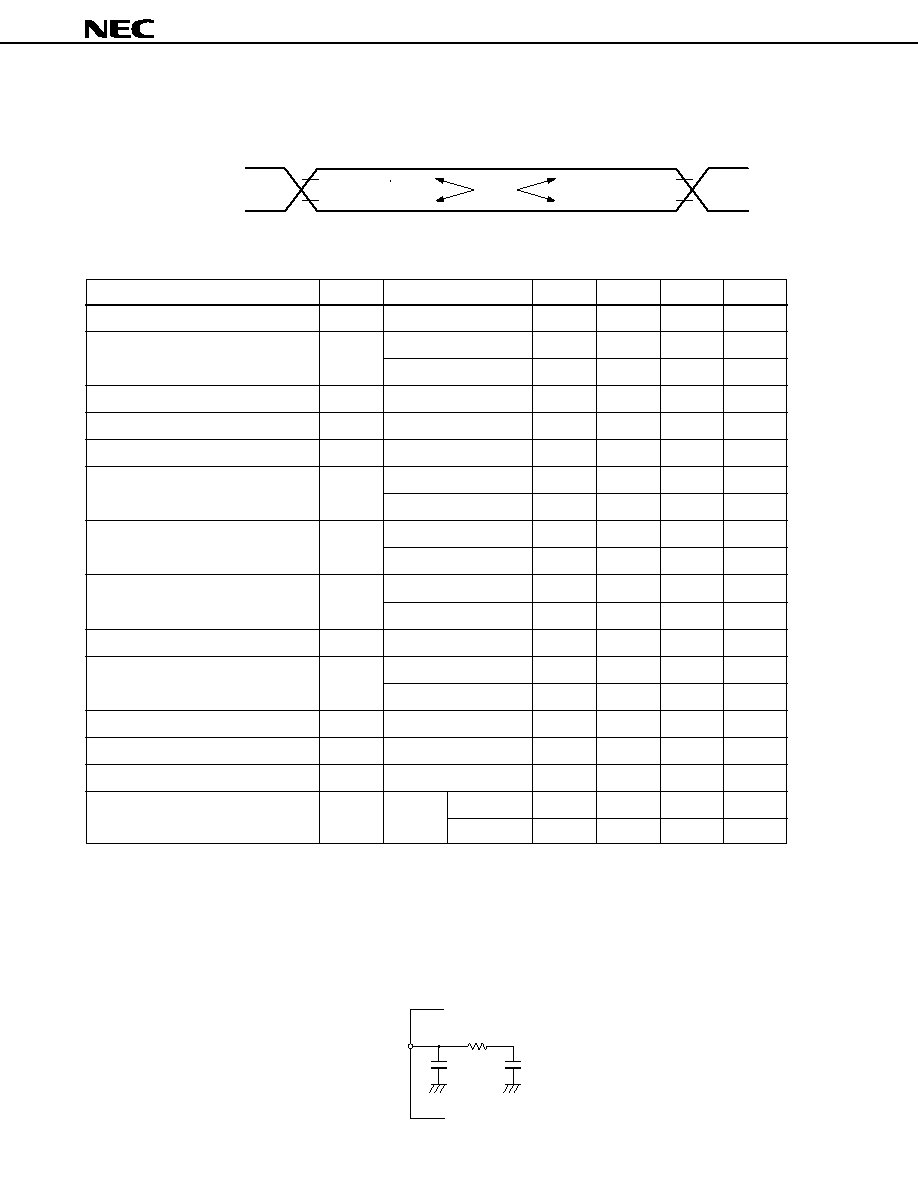
PIN I/O CIRCUIT AND UNUSED-PIN PROCESSING
The I/O circuits of the pins are shown in Table 1-1 and Figure 1-1 some of them in a simplified form.
Table 1-1. I/O Circuit Types of Pins and Recommended Connection Methods When Unused
Pin Name
P00/RTP0-P07/RTP7
P20/NMI
P21/INTP0-P26/INTP5
P27/INTP6/TI
P30/T
X
D
P31/R
X
D
P32/SO/SB0
P33/SI/SB1
P34/SCK
P40/AD0-P47/AD7
P50/A8-P57/A15
P70/AN0-P77/AN7
P80/TO00-P83/TO03
P84/TO10, P85/TO11
P90/RD
P91/WR
P92/TAS
P93/TMD
WDTO
ASTB
EA
RESET
AV
DD
AV
REF
AV
SS
V
PP
NC
I/O Circuit Type
5
2
5
8
5
9
5
5
3
4
1
2
--
--
--
--
Recommended Connection Method When Unused
Input status: Connected to V
DD
or V
SS
via a resistor individually.
Output status: No connection required.
Connected to V
SS
.
Input status: Connected to V
DD
or V
SS
via a resistor individually.
Output status: No connection required.
Connected to Vss.
Input status: Connected to V
DD
or Vss via a resistor individually.
Output status: No connection required.
No connection required.
--
--
Connected to V
DD
.
Connected to V
SS
.
Connected to V
DD
.
Connected to V
SS
. (It is also possible to leave this unconnected.)
µ
PD78P324, 78P324(A)
15
Figure 1-1. I/O Circuits of Pins
Type 1
Type 5
Type 2
Type 8
Type 3
Type 9
Type 4
This is a Schmitt-triggered input which has the hysteresis
characteristic.
This is the push-pull input which is capable of output high-
impedance (off for both P-ch and N-ch).
V
DD
P-ch
N-ch
IN
IN
P-ch
N-ch
OUT
V
DD
P-ch
N-ch
OUT
V
DD
output
disable
data
IN
P-ch
N-ch
Comparator
V
ref
(Threshold voltage)
input
enable
P-ch
N-ch
V
DD
IN/OUT
output
disable
data
P-ch
N-ch
V
DD
output
disable
data
IN/OUT
input
disable
µ
PD78P324, 78P324(A)
16
2.
DIFFERENCES BETWEEN
µ
PD78P324 AND
µ
PD78324
The
µ
PD78P324 is a product in which the
µ
PD78324's internal mask ROM is replaced by a 32KB PROM.
Therefore, these two products share the same functions, except for differences deriving from the ROM
specifications (for example, Write and Verify, etc.). Their differences are shown in Table 2-1 below.
Table 2-1. Differences between
µ
PD78P324 and
µ
PD78324
Product Name
Parameter
Internal program memory
(Electric write)
ECC circuit
PROM programming pin
Package
Electrical characteristics
Others
Cautions
1. The PROM product and the mask ROM product differ in their noise resistance volume and noise
reflection. If replacement of the PROM product with the mask ROM product in the process of trial
to mass production is being considered, ensure to make a sufficient evaluation with the CS
product (not ES product) of the mask ROM product.
2. The
µ
PD78P324(A)/(A1)/(A2) are one-time PROM products only. The differences between the
µ
PD78P324(A)/(A1)/(A2) and the
µ
PD78324(A)/(A1)/(A2) are the same as those shown in the table
above, except in terms of the EPROM product.
µ
PD78P324
µ
PD78324
One-time PROM
EPROM
Mask ROM
(Write enabled only once)
(Rewrite enabled)
With
Without
With
Without
∑ 68-pin plastic QFJ
∑ 68-pin ceramic WQFN
∑ 68-pin plastic QFJ
∑ 74-pin plastic QFP
∑ 74-pin ceramic WQFN
∑ 74-pin plastic QFP
Differ in current consumption, etc.
As they differ in their circuit size and mask layout, their noise resistance volume and
noise reflection differ.

µ
PD78P324, 78P324(A)
17
3.
PROM PROGRAMMING
The
µ
PD78P324 incorporates an electrically writable 32768-by-8-bit program PROM and an 8192-by-6-bit
ECC (error correcting code) PROM.
ECC corrects the errors in codes written in the program PROM, thus improving the reliability of the PROM
content. Figure 3-1 shows the memory map in programming mode.
Figure 3-1. Memory Map in Programming Mode
ECC (for ECW)
ECW
(4 x 8)
PROM for ECC
Note
(8192 x 6)
Program PROM
(32768 x 8)
A004H
A003H
A000H
9FFFH
8000H
7FFFH
0000H
Note
On the ECC PROM, the lower 6 bits are valid.
When programming, set the RESET pin and the AV
DD
pin to PROM programming mode. The programming
characteristics of the
µ
PD78P324 are compatible with the
µ
PD27C1001A. However, the programming mode
is compatible only with the byte program mode of the
µ
PD27C1001A. For setting on the PROM programmer,
please select the byte program mode of the 27C1001A mode.
When using the ECC circuit, reset the lowest bit (A000.0) of the lowest byte of the ECW (ECC control word)
to enable the operation of the ECC circuit. ECW is a 4-byte register which controls the operation of the ECC
circuit. ECC and ECW are generated automatically with the ECCGEN (ECC generator) which comes with the
RA78K3 assembler package. (ECC is generated in the lower 6 bits; and the upper 2 bits are fixed to 1.)
µ
PD78P324, 78P324(A)
18
Table 3-1. Pin Functions in Programming Mode
Function
Normal Operation Mode
Programming Mode
Address input
P00-P07, P80, P20, P81-P85, P33, P34
A0-A16
Data input
P40-P47
D0-D07
Program pulse
P32
PGM
Chip enable
P31
CE
Output enable
P30
OE
Program voltage
V
PP
Mode voltage
RESET, AV
DD
3.1
OPERATION MODE
When placing the microcomputer in programming Write/Verify mode, set it to RESET = H and AV
DD
= L.
In this mode, an operation mode in Table 3-2 can be selected by further setting the CE and OE pins.
When reading the content of the PROM, set it to Read mode. Process the unused pins in accordance with
the instructions in the PIN CONFIGURATION.
Table 3-2. Operation Mode of PROM Programming
Mode
Program Write
Program verify
Program inhibit
Read
Output disable
Standby
RESET
H
AV
DD
L
Remark
x: L or H
CE
L
L
X
X
L
L
H
OE
H
L
L
H
L
H
X
PGM
L
H
L
H
H
X
X
V
PP
+12.5 V
+5 V
V
DD
+6.5 V
+5 V
D0-D7
Data input
Data output
High impedance
Data output
High impedance
High impedance
µ
PD78P324, 78P324(A)
19
3.2
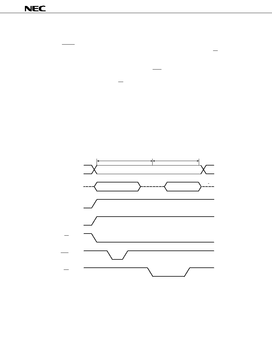
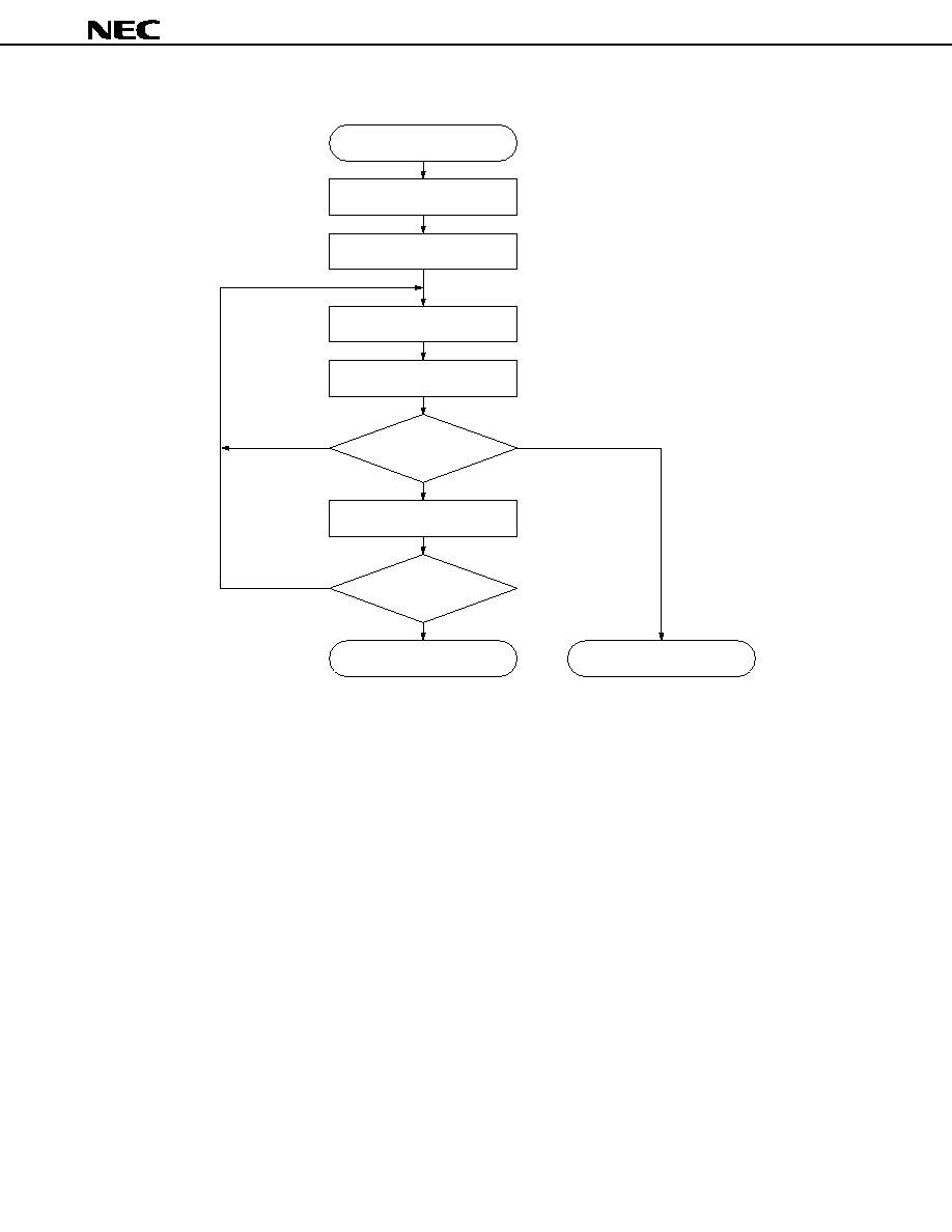
PROCEDURE FOR PROM WRITE
The procedure for writing into the PROM is as follows (see Figure 3-3).
(1) Fix to RESET = H; and AV
DD
= L. Other unused pins are processed as directed by the PIN CONFIGURATION.
(2) Supply +6.5 V to the V
DD
pin; and +12.5 V to the V
PP
pin. Enter the low level into the CE pin.
(3) Enter the initial address into A0-A16.
(4) Enter the Write data into D0-D7.
(5) Enter the 0.1 ms program pulse (active low) into the PGM pin.
(6) Verify mode. Check if the Write data has been written or not.
Enter the active low pulse into the OE pin and read the Write data from D0-D7.
∑ When written: Move to (8).
∑ When not able to write: Repeat (4) to (6). If it is not possible to write even when the repetition has been
made ten times, move to (7).
(7) Stop the Write operation as a defective device.
(8) Increment the address.
(9) Repeat (4) to (8) until the final address.
The timing of the above (2) to (7) steps is shown in Figure 3-2.
Figure 3-2. PROM Write/Verify Timing
Hi-Z
Hi-Z
Hi-Z
Program
Program verify
Address input
Data input
Data output
A0-A16
D0-D7
V
PP
V
DD
CE (input)
PGM (input)
OE (input)
+ 12.5V
V
DD
+ 6.5V
V
DD
µ
PD78P324, 78P324(A)
20
Figure 3-3. Write Procedure Flowchart
Start writing
Supply the supply voltage
Supply the initial address
Supply the Write data
Supply the program pulse
Write disabled
( less than 10 times )
Verify mode
Address increment
Write disabled
( 10th times )
Write complete
Defective device
Final address
>Final address
Final address
Write OK
(10)
(9)
(8)
(6)
(5)
(4)
(3)
(2)
(1)
(7)

µ
PD78P324, 78P324(A)
21
3.3
PROCEDURE FOR PROM READ
The PROM content is read to the external data bus (D0-D7) in accordance with the following procedure:
(1) Fix to RESET = H; and AV
DD
= L. Other unused pins are processed as directed by the PIN CONFIGURATION.
(2) Supply +5 V to the V
DD
and V
PP
pins.
(3) Enter the address of the data read into the A0-A16 pin.
(4) Read mode (CE = L; OE = L)
(5) Data is output to the D0-D7 pin.
The timing of the above (2) to (5) is shown in Figure 3-4.
Figure 3-4. PROM Read Timing
Address input
Data output
A0-A14
CE (input)
OE (input)
D0-D7
Hi-Z
Hi-Z
µ
PD78P324, 78P324(A)
22
4.
ERASURE CHARACTERISTICS (
µ
PD78P324KC/KD ONLY)
The
µ
PD78P324KC/KD can erase (FFH) the content of the data written in the program memory and perform
rewriting.
The data content is erased by radiating light with a wavelength shorter than about 400 nm on the erasure
window. Normally, ultraviolet light with a wavelength of 254 nm is radiated. The volume of light required
for erasing the data content completely is as follows:
∑ Ultraviolet ray intensity x erasure time: 15 W∑s/cm
2
or more
∑ Erasure time: 15 to 20 mins (This is so when using an ultraviolet lamp of 12,000
µ
W/cm
2
. However, a
longer time may be required due to performance degradation of the ultraviolet ray lamp or dirt
deposited on the erasure window, etc.)
For erasure, make sure to place the ultraviolet ray lamp at a location within 2.5 cm from the erasure
window. If the ultraviolet ray lamp is equipped with a filter, make sure that the filter is removed for radiation.
5.
ERASURE WINDOW SEAL (
µ
PD78P324KC/KD ONLY)
If the erasure window part of the
µ
PD78P324KC/KD is exposed to sunlight or fluorescent light for too long,
the EPROM data may be erased or the internal circuits may malfunction. To prevent such an accident, please
ensure that the erasure window part is covered with a protective seal except when the data is going to be
erased.
The EPROM package with window is shipped with a protective seal that is NEC's guarantee of quality.
6.
ONE-TIME PROM PRODUCT SCREENING
Structurally, it is not possible for NEC to test the one-time PROM products (
µ
PD78P324GJ-5BJ/(A)/(A1)/
(A2) and 78P324LP/(A)/(A1)/(A2) completely before shipment. Therefore, it recommended that, after writing
the required data, the screening be implemented to verify the PROM after storing the product in the
following temperature and condition.
Storage Temperature
Storage Time
125
∞
C
24 hrs
NEC provides at a charge services including the one-time PROM writing, sealing, screening and verifying
under the title of QTOP microcomputer. For further details, please contact an NEC salesperson.

µ
PD78P324, 78P324(A)
23
7.
ELECTRICAL SPECIFICATIONS
(1)
µ
PD78P324 Electrical Specifications (1/9)
Absolute Maximum Ratings (T
A
= 25
∞
C)
Parameter
Supply voltage
Input voltage
Output voltage
Low-level output current
High-level output current
Analog input voltage
A/D converter reference input voltage
Operating ambient temperature
Storage temperature
Unit
V
V
V
V
V
V
mA
mA
mA
mA
V
V
∞
C
∞
C
Rating
≠0.5 to +7.0
≠0.5 to V
DD
+0.5
≠0.5 to +13.5
≠0.5 to +0.5
≠0.5 to V
DD
+0.5
≠0.5 to V
DD
+0.5
4.0
90
≠1.0
≠20
≠0.5 to V
DD
+0.5
≠0.5 to AV
DD
+0.5
≠0.5 to V
DD
+0.5
≠0.5 to AV
DD
+0.5
≠10 to +70
≠65 to +150
Symbol
V
DD
AV
DD
V
PP
AV
SS
V
I
V
O
I
OL
I
OH
V
IAN
AV
REF
T
A
T
stg
Condition
Note 1
All output pins
Total of all output pins
All output pins
Total of all output pins
AV
DD
> V
DD
Note 2
V
DD
AV
DD
AV
DD
> V
DD
V
DD
AV
DD
Notes 1. Except P70/AN0-P77/AN7.
2. P70/AN0-P77/AN7 pins.
Caution
If the absolute maximum rating of any one of the parameters is exceeded even momentarily, the
quality of the product may be degraded. In other words, the product may be physically damaged
if any of the absolute maximum ratings is exceeded. Be sure to use the product without exceeding
these ratings.
Recommended Operating Range
Oscillation Frequency
T
A
V
DD
8MHz
f
XX
16MHz
≠10 to +70
∞
C
+5.0 V
±
10 %
Capacitance (T
A
= 25
∞
C, V
SS
= V
DD
= 0 V)
Parameter
Input capacitance
Output capacitance
I/O capacitance
Symbol
C
I
C
O
C
IO
Condition
f = 1 MHz;
0 V except measured pins
MIN.
TUP.
MAX.
Unit
10
pF
20
pF
20
pF

µ
PD78P324, 78P324(A)
24
(1)
µ
PD78P324 Electrical Specifications (2/9)
Oscillator Characteristics (T
A
= ≠10 to +70
∞
C, V
DD
= +5 V
±
10 %, V
SS
= 0 V)
Oscillator
Ceramic oscillator or
crystal oscillator
External clock
Recommended Circuit
Parameter
Oscillation frequency (f
XX
)
X1 input frequency (f
X
)
X1 input rise time, fall time
(t
XR
, t
XF
)
X1 input high-/low-level
width (t
WXH
, t
WXL
)
MIN.
MAX.
Unit
8
16
MHz
8
16
MHz
0
20
ns
25
80
ns
Caution
When using the system clock oscillation circuit, wire the part encircled in the dotted line in the
following manner to avoid the influence of the wiring capacity, etc.
∑ Make the wiring as short as possible.
∑ Avoid intersecting other signal conductors. Avoid approaching lines in which very high fluctuating
currents run.
∑ Make sure that the grounding point of the oscillation circuit capacitor always has the same
electrical potential as V
SS
. Avoid grounding with a grand pattern in which very high currents run.
∑ Do not fetch signals from the oscillation circuit.
X2
X1
V
SS
C2
C1
X2
X1
X2
X1
HCMOS
inverter
HCMOS
inverter
or
No connection
required
µ
PD78P324, 78P324(A)
25
(1)
µ
PD78P324 Electrical Specifications (3/9)
Recommended Oscillation Circuit Constants
Ceramic Oscillator
Recommended Constant
C1 (pF)
C2 (pF)
30
30
15
15
Incorporated
Incorporated
Product Name
CSA8.00MT
CSA12.0MT
CSA14.74MXZ040
CSA16.00MX040
CST8.00MTW
CST12.0MTW
CST14.74MXW0C3
CST16.00MXW0C3
Frequency (MHz)
8.0
12.0
14.74
16.0
8.0
12.0
14.74
16.0
Manufacturer
Murata Mfg. Co., Ltd.

µ
PD78P324, 78P324(A)
26
(1)
µ
PD78P324 Electrical Specifications (4/9)
DC Characteristics (T
A
= ≠10 to +70
∞
C, V
DD
= +5 V
±
10 %, V
SS
= 0 V)
Parameter
Low-level input voltage
High-level input voltage
Low-level output voltage
High-level output voltage
Input leakage current
Analog pin input leakage current
Output leakage current
V
DD
supply current
Data retention voltage
Data retention current
MIN.
TYP.
MAX.
Unit
0
0.8
V
2.2
V
0.8 V
DD
0.45
V
V
DD
≠1.0
V
±
10
µ
A
±
10
µ
A
±
10
µ
A
70
95
mA
35
55
mA
2.5
V
2
10
µ
A
10
50
µ
A
Symbol
V
IL
V
IH1
V
IH2
V
OL
V
OH
I
LI
I
LIAN
I
LO
I
DD1
I
DD2
V
DDDR
I
DDDR
Condition
Note 1
Note 2
I
OL
= 2.0mA
I
OH
= ≠400
µ
A
Note 3
0 V
V
I
V
DD
Note 4
0 V
V
IAN
AV
REF
0 V
V
O
V
DD
Operation mode
HALT mode
STOP mode
V
DDDR
= 2.5 V
STOP mode
V
DDDR
=5.0 V
±
10%
Notes 1. Pins other than pins in Note 2.
2. RESET, X1, X2, P20/NMI, P21/INTP0, P22/INTP1, P23/INTP2, P24/INTP3, P25/INTP4, P26/INTP5, P27/
INTP6/TI, P32/SO/SB0, P33/SI/SB1, P34/SCK pins.
3. Pins except P20/NMI, EA/V
PP
, X1, X2
4. When not sampling the analog input

µ
PD78P324, 78P324(A)
27
(1)
µ
PD78P324 Electrical Specifications (5/9)
AC Characteristics (T
A
= ≠10 to +70
∞
C, V
DD
= +5 V
±
10%, V
SS
= 0 V, C
L
= 100pF)
Non-serial Read/Write Operation (when connecting general-purpose memory)
Parameter
Symbol
Condition
MIN.
MAX.
Unit
System clock cycle time
t
CYK
125
250
ns
Address setup time (vs. ASTB
)
t
SAST
32
ns
Address hold time (vs. ASTB
)
t
HSTA
32
ns
Address
RD
delay time
t
DAR
85
ns
RD
address float time
t
FRA
10
ns
Address
data input time
t
DAID
222
ns
RD
data input time
t
DRID
112
ns
ASTB
RD
delay time
t
DSTR
42
ns
Data hold time (vs. RD
)
t
HRID
0
ns
RD
address active time
t
DRA
50
ns
RD low-level width
t
WRL
147
ns
ASTB high-level width
t
WSTH
37
ns
Address
WR
delay time
t
DAW
85
ns
ASTB
data output time
t
DSTOD
102
ns
WR
data output time
t
DWOD
40
ns
ASTB
WR
delay time
t
DSTW
42
ns
Data setup time (vs. WR
)
t
SODW
147
ns
Data hold time (vs. WR
)
t
HWOD
32
ns
WR
ASTB
delay time
t
DWST
42
ns
WR low-level width
t
WWL
147
ns
µ
PD78P324, 78P324(A)
28
(1)
µ
PD78P324 Electrical Specifications (6/9)
t
CYK
-dependent Bus Timing Definition
Symbol
Calculation formula
MIN./MAX.
Unit
t
SAST
0.5T≠30
MIN.
ns
t
HSTA
0.5T≠30
MIN.
ns
t
DAR
T≠40
MIN.
ns
t
DAID
(2.5+n) T≠90
MAX.
ns
t
DRID
(1.5+n) T≠75
MAX.
ns
t
DSTR
0.5T≠20
MIN.
ns
t
DRA
0.5T≠12
MIN.
ns
t
WRL
(1.5+n) T≠40
MIN.
ns
t
WSTH
0.5T≠25
MIN.
ns
t
DAW
T≠40
MIN.
ns
t
DSTOD
0.5T+40
MAX.
ns
t
DSTW
0.5T≠20
MIN.
ns
t
SODW
1.5T≠40
MIN.
ns
t
HWOD
0.5T≠30
MIN.
ns
t
DWST
0.5T≠20
MIN.
ns
t
WWL
(1.5+n) T≠40
MIN.
ns
Remarks
1. T = t
CYK
= 1/f
CLK
(f
CLK
refers to the internal system clock frequency)
2. n refers to the count of weight cycles defined by the user software.
3. Among the parameters for bus timing, only those listed in this table are dependent on t
CYK
.

µ
PD78P324, 78P324(A)
29
(1)
µ
PD78P324 Electrical Specifications (7/9)
Serial Operation (T
A
= ≠10 to +70
∞
C, V
DD
= +5 V
±
10 %, V
SS
= 0 V)
Parameter
Symbol
Condition
MIN.
MAX.
Unit
SCK output
Internal divide-by-eight
1
µ
s
Serial clock cycle time
t
CYSK
SCK input
External clock
1
µ
s
SCK output
Internal divide-by-eight
420
ns
Serial clock low-level width
t
WSKL
SCK input
External clock
420
ns
SCK output
Internal divide-by-eight
420
ns
Serial clock high-level width
t
WSKH
SCK input
External clock
420
ns
SI setup time (vs. SCK
)
t
SRXSK
80
ns
SI hold time (vs. SCK
)
t
HSKRX
80
ns
SCK
SO delay time
t
DSKTX
R = 1 k
, C = 100pF
210
ns
t
CYK
-dependent Serial Operation
Symbol
Condition
Calculation Formula
MIN./MAX.
Unit
SCK output
Internal divide-by-eight
8T
MIN.
ns
t
CYSK
SCK input
External clock
8T
MIN.
ns
SCK output
Internal divide-by-eight
4T≠80
MIN.
ns
t
WSKL
SCK input
External clock
4T≠80
MIN.
ns
SCK output
Internal divide-by-eight
4T≠80
MIN.
ns
t
WSKH
SCK input
External clock
4T≠80
MIN.
ns
Remarks
1. T = t
CYK
= 1/f
CLK
(f
CLK
refers to the internal system clock frequency)
2. Among the parameters for serial operation, only those listed in this table are dependent on t
CYK
.

µ
PD78P324, 78P324(A)
30
(1)
µ
PD78P324 Electrical Specifications (8/9)
Other Operations (T
A
= ≠10 to +70
∞
C, V
DD
= +5 V
±
10 %, V
DD
= 0 V)
Parameter
Symbol
Condition
MIN.
MAX.
Unit
NMI high-/low-level width
t
WNIH
, t
WNIL
Analog noises removed
4
µ
s
INTP0 high-/low-level width
t
WIOH
, t
WIOL
1
µ
s
INTP1 high-/low-level width
t
WI1H
, t
WI1L
1
µ
s
INTP2 high-/low-level width
t
WI2H
, t
WI2L
1
µ
s
INTP3 high-/low-level width
t
WI3H
, t
WI3L
1
µ
s
INTP4 high-/low-level width
t
WI4H
, t
WI4L
1
µ
s
INTP5 high-/low-level width
t
WI5H
, t
WI5L
1
µ
s
INTP6 high-/low-level width
t
WI6H
, t
WI6L
1
µ
s
RESET high-/low-level width
t
WRSH
, t
WRSL
Analog noises removed
3.5
µ
s
TI high-/low-level width
t
WTIH
, t
WTIL
1
µ
s
V
DD
rise/fall time
t
RVD
, t
FVD
200
µ
s
Other t
CYK
-dependent Operations
Symbol
Calculation formula
MIN./MAX.
Unit
t
WIOH
8T
MIN.
ns
t
WIOL
8T
MIN.
ns
t
WI1H
8T
MIN.
ns
t
WI1L
8T
MIN.
ns
t
WI2H
8T
MIN.
ns
t
WI2L
8T
MIN.
ns
t
WI3H
8T
MIN.
ns
t
WI3L
8T
MIN.
ns
t
WI4H
8T
MIN.
ns
t
WI4L
8T
MIN.
ns
t
WI5H
8T
MIN.
ns
t
WI5L
8T
MIN.
ns
t
WI6H
8T
MIN.
ns
t
WI6L
8T
MIN.
ns
t
WTIH
8T
MIN.
ns
t
WTIL
8T
MIN.
ns
Remarks
1. T = t
CYK
= 1/f
CLK
(f
CLK
refers to the internal system clock frequency)
2. Only the parameters listed in this table depend on t
CYK
.
µ
PD78P324, 78P324(A)
31
(1)
µ
PD78P324 Electrical Specifications (9/9)
AC Timing Test Point
A/D Converter Characteristics (T
A
= ≠10 to +70
∞
C, V
DD
= +5 V
±
10 %, V
SS
= AV
SS
= 0 V, V
DD
≠0.5 V
AV
DD
V
DD
)
Parameter
Resolution
Total error
Note1
Quantization error
Conversion time
Sampling time
Zero-scale error
Note1
Full-scale error
Note 1
Non-linear error
Note 1
Analog input voltage
Note 2
Analog input impedance
Reference voltage
AV
REF
current
AV
DD
supply current
A/D converter data retention current
MIN.
TYP.
MAX.
Unit
10
bit
±
0.4
%FSR
±
0.7
%FSR
±
1/2
LSB
144
t
CYK
24
t
CYK
±
1.5
±
2.5
LSB
±
1.5
±
4.5
LSB
±
1.5
±
2.5
LSB
±
1.5
±
4.5
LSB
±
1.5
±
2.5
LSB
±
1.5
±
4.5
LSB
0
AV
DD
V
10
M
Note 3
3.4
AV
DD
V
1.0
3.0
mA
2.0
6.0
mA
2
15
µ
A
10
50
µ
A
Symbol
t
CONV
t
SAMP
V
IAN
R
AN
AV
REF
AI
REF
AI
DD
AI
DDDR
Condition
4.5 V
AV
REF
AV
DD
3.5 V
AV
REF
AV
DD
4.5 V
AV
REF
AV
DD
3.4 V
AV
REF
AV
DD
4.5 V
AV
REF
AV
DD
3.4 V
AV
REF
AV
DD
4.5 V
AV
REF
AV
DD
3.4 V
AV
REF
AV
DD
When not sampled
When sampled
Operation mode
AV
DDDR
= 2.5 V
STOP mode
AV
DDDR
=5 V
±
10%
Notes 1. Quantization error excluded.
2. When ≠0.3 V
V
IAN
0 V, the conversion result becomes 000H.
When 0 V < V
IAN
< AV
REF
, the conversion is performed at a resolution of 10 bits.
When AV
REF
V
IAN
AV
DD
, the conversion result is 3FFH.
3. The analog input impedance in sampling is the same as the equivalent circuit shown in the diagram
below. (The values in the diagram are TYP. values; therefore, they are not assured.)
0.8V
DD
or 2.2V
0.8V
0.8V
DD
or 2.2V
0.8V
Test point
V
DD
0V
20k
10pF
30pF
Analog input pin
( input
capacitance
included )

µ
PD78P324, 78P324(A)
32
(2)
µ
PD78P324(A) Electrical Specifications (1/9)
Absolute Maximum Ratings (T
A
= 25
∞
C)
Parameter
Supply voltage
Input voltage
Output voltage
Low-level output current
High-level output current
Analog input voltage
A/D converter reference input voltage
Operating ambient temperature
Storage temperature
Unit
V
V
V
V
V
V
mA
mA
mA
mA
V
V
∞
C
∞
C
Rating
≠0.5 to +7.0
≠0.5 to V
DD
+0.5
≠0.5 to +13.5
≠0.5 to +0.5
≠0.5 to V
DD
+0.5
≠0.5 to V
DD
+0.5
4.0
90
≠1.0
≠20
≠0.5 to V
DD
+0.5
≠0.5 to AV
DD
+0.5
≠0.5 to V
DD
+0.5
≠0.5 to AV
DD
+0.5
≠40 to +85
≠65 to +150
Symbol
V
DD
AV
DD
V
PP
AV
SS
V
I
V
O
I
OL
I
OH
V
IAN
AV
REF
T
A
T
stg
Condition
Notes 1, 2
All output pins
Total of all output pins
All output pins
Total of all output pins
AV
DD
> V
DD
Notes 2, 3
V
DD
AV
DD
AV
DD
> V
DD
V
DD
AV
DD
Notes 1. Except P70/AN0-P77/AN7.
2. The overvoltage condition of the allowable pin injectioncurrent characteristics in overvoltage application
is excluded.
3. P70/AN0-P77/AN7 pins.
Caution
If the absolute maximum rating of any one of the parameters is exceeded even momentarily, the
quality of the product may be degraded. In other words, the product may be physically damaged
if any of the absolute maximum ratings is exceeded. Be sure to use the product without exceeding
these ratings.

µ
PD78P324, 78P324(A)
33
(2)
µ
PD78P324(A) Electrical Specifications (2/9)
Permissible Pin Injection Current Characteristics in Overvoltage Application (T
A
= ≠40 to +85
∞
C, V
DD
= +5 V
±
10%, V
SS
= 0 V)
Parameter
Positive
injection
current
(V
IN
> V
DD
)
Negative
injection
current
(V
IN
< V
SS
)
Symbol
I
IJH1
I
IJH2
I
IJH
I
IJL1
I
IJL2
I
IJL
MIN.
TYP.
MAX.
Unit
10
mA
0.5
mA
3
mA
1
mA
100
mA
5
mA
≠4
mA
≠0.4
mA
≠4
mA
≠0.3
mA
≠40
mA
≠3
mA
Condition
Peak value
Mean value
1 pin
Peak value
Mean value
Peak value
Total of all input pins
Mean value
Peak value
Mean value
1 pin
Peak value
Mean value
Peak value
Total of all input pins
Mean value
Input ports other
than ANn (n = 0-7)
ANn (n = 0-7)
Input ports other
than ANn (n = 0-7)
ANn (n = 0-7)
Cautions
1. When the injection current has run into the analog input pin (ANn: n = 0-7), the A/D conversion
result of the analog input contiguous to the current injection pin has the value of the standard
in which the injection current is not running plus
±
2LSB.
2. The mean value (absolute value) of the pin injected current is as follows:
Mean value = ((1/T)
| i(t) |
3/2
dt)
2/3
In this, i(t) refers to the pin injected current. The maximum value of |i(t)| is the peak value.
Recommended Operating Range
Oscillation Frequency
T
A
V
DD
8MHz
f
XX
16MHz
≠40 to +85
∞
C
+5.0 V
±
10 %
Capacitance (T
A
= 25
∞
C, V
SS
= V
DD
= 0 V)
Parameter
Input capacitance
Output capacitance
I/O capacitance
Symbol
C
I
C
O
C
IO
Condition
f = 1 MHz;
0 V except measured pins
MIN.
TUP.
MAX.
Unit
10
pF
20
pF
20
pF
T
0
µ
PD78P324, 78P324(A)
34
(2)
µ
PD78P324(A) Electrical Specifications (3/9)
Oscillator Characteristics (T
A
= ≠40 to +85
∞
C, V
DD
= +5 V
±
10 %, V
SS
= 0 V)
Oscillator
Ceramic oscillator or
crystal oscillator
External clock
Recommended Circuit
Parameter
Oscillation frequency (f
XX
)
X1 input frequency (f
X
)
X1 input rise time, fall time
(t
XR
, t
XF
)
X1 input high-/low-level
width (t
WXH
, t
WXL
)
MIN.
MAX.
Unit
8
16
MHz
8
16
MHz
0
20
ns
25
80
ns
Caution
When using the system clock oscillation circuit, wire the part encircled in the dotted line in the
following manner to avoid the influence of the wiring capacity, etc.
∑ Make the wiring as short as possible.
∑ Avoid intersecting other signal conductors. Avoid approaching lines in which very high fluctuating
currents run.
∑ Make sure that the grounding point of the oscillation circuit capacitor always has the same
electrical potential as V
SS
. Avoid grounding with a grand pattern in which very high currents run.
∑ Do not fetch signals from the oscillation circuit.
X2
X1
V
SS
C2
C1
X2
X1
X2
X1
HCMOS
inverter
HCMOS
inverter
or
No connection
required

µ
PD78P324, 78P324(A)
35
(2)
µ
PD78P324(A) Electrical Specifications (4/9)
DC Characteristics (T
A
= ≠40 to +85
∞
C, V
DD
= +5 V
±
10 %, V
SS
= 0 V)
Parameter
Low-level input voltage
High-level input voltage
Low-level output voltage
High-level output voltage
Input leakage current
Analog pin input leakage current
Output leakage current
V
DD
supply current
Data retention voltage
Data retention current
MIN.
TYP.
MAX.
Unit
0
0.8
V
2.2
V
0.8 V
DD
0.45
V
V
DD
≠1.0
V
±
10
µ
A
±
1
µ
A
±
10
µ
A
70
95
mA
35
55
mA
2.5
V
2
10
µ
A
10
50
µ
A
Symbol
V
IL
V
IH1
V
IH2
V
OL
V
OH
I
LI
I
LIAN
I
LO
I
DD1
I
DD2
V
DDDR
I
DDDR
Condition
Note 1
Note 2
I
OL
= 2.0mA
I
OH
= ≠400
µ
A
Note 3
0 V
V
I
V
DD
Note 4
0 V
V
IAN
AV
REF
0 V
V
O
V
DD
Operation mode
HALT mode
STOP mode
V
DDDR
= 2.5 V
STOP mode
V
DDDR
=5.0 V
±
10%
Notes 1. Pins other than pins in Note 2.
2. RESET, X1, X2, P20/NMI, P21/INTP0, P22/INTP1, P23/INTP2, P24/INTP3, P25/INTP4, P26/INTP5, P27/
INTP6/TI, P32/SO/SB0, P33/SI/SB1, P34/SCK pins.
3. Pins except P20/NMI, EA/V
PP
, X1, X2
4. When not sampling the analog input

µ
PD78P324, 78P324(A)
36
(2)
µ
PD78P324(A) Electrical Specifications (5/9)
AC Characteristics (T
A
= ≠40 to +85
∞
C, V
DD
= +5 V
±
10%, V
SS
= 0 V, C
L
= 100pF)
Non-serial Read/Write Operation (when connecting general-purpose memory)
Parameter
Symbol
Condition
MIN.
MAX.
Unit
System clock cycle time
t
CYK
125
250
ns
Address setup time (vs. ASTB
)
t
SAST
32
ns
Address hold time (vs. ASTB
)
t
HSTA
32
ns
Address
RD
delay time
t
DAR
85
ns
RD
address float time
t
FRA
10
ns
Address
data input time
t
DAID
222
ns
RD
data input time
t
DRID
112
ns
ASTB
RD
delay time
t
DSTR
42
ns
Data hold time (vs. RD
)
t
HRID
0
ns
RD
address active time
t
DRA
50
ns
RD low-level width
t
WRL
147
ns
ASTB high-level width
t
WSTH
37
ns
Address
WR
delay time
t
DAW
85
ns
ASTB
data output time
t
DSTOD
102
ns
WR
data output time
t
DWOD
40
ns
ASTB
WR
delay time
t
DSTW
42
ns
Data setup time (vs. WR
)
t
SODW
147
ns
Data hold time (vs. WR
)
t
HWOD
32
ns
WR
ASTB
delay time
t
DWST
42
ns
WR low-level width
t
WWL
147
ns

µ
PD78P324, 78P324(A)
37
(2)
µ
PD78P324(A) Electrical Specifications (6/9)
t
CYK
-dependent Bus Timing Definition
Symbol
Calculation formula
MIN./MAX.
Unit
t
SAST
0.5T≠30
MIN.
ns
t
HSTA
0.5T≠30
MIN.
ns
t
DAR
T≠40
MIN.
ns
t
DAID
(2.5+n) T≠90
MAX.
ns
t
DRID
(1.5+n) T≠75
MAX.
ns
t
DSTR
0.5T≠20
MIN.
ns
t
DRA
0.5T≠12
MIN.
ns
t
WRL
(1.5+n) T≠40
MIN.
ns
t
WSTH
0.5T≠25
MIN.
ns
t
DAW
T≠40
MIN.
ns
t
DSTOD
0.5T+40
MAX.
ns
t
DSTW
0.5T≠20
MIN.
ns
t
SODW
1.5T≠40
MIN.
ns
t
HWOD
0.5T≠30
MIN.
ns
t
DWST
0.5T≠20
MIN.
ns
t
WWL
(1.5+n) T≠40
MIN.
ns
Remarks
1. T = t
CYK
= 1/f
CLK
(f
CLK
refers to the internal system clock frequency)
2. n refers to the count of weight cycles defined by the user software.
3. Among the parameters for bus timing, only those listed in this table are dependent on t
CYK
.

µ
PD78P324, 78P324(A)
38
(2)
µ
PD78P324(A) Electrical Specifications (7/9)
Serial Operation (T
A
= ≠40 to +85
∞
C, V
DD
= +5 V
±
10 %, V
SS
= 0 V)
Parameter
Symbol
Condition
MIN.
MAX.
Unit
SCK output
Internal divide-by-eight
1
µ
s
Serial clock cycle time
t
CYSK
SCK input
External clock
1
µ
s
SCK output
Internal divide-by-eight
420
ns
Serial clock low-level width
t
WSKL
SCK input
External clock
420
ns
SCK output
Internal divide-by-eight
420
ns
Serial clock high-level width
t
WSKH
SCK input
External clock
420
ns
SI setup time (vs. SCK
)
t
SRXSK
80
ns
SI hold time (vs. SCK
)
t
HSKRX
80
ns
SCK
SO delay time
t
DSKTX
R = 1 k
, C = 100pF
210
ns
t
CYK
-dependent Serial Operation
Symbol
Condition
Calculation Formula
MIN./MAX.
Unit
SCK output
Internal divide-by-eight
8T
MIN.
ns
t
CYSK
SCK input
External clock
8T
MIN.
ns
SCK output
Internal divide-by-eight
4T≠80
MIN.
ns
t
WSKL
SCK input
External clock
4T≠80
MIN.
ns
SCK output
Internal divide-by-eight
4T≠80
MIN.
ns
t
WSKH
SCK input
External clock
4T≠80
MIN.
ns
Remarks
1. T = t
CYK
= 1/f
CLK
(f
CLK
refers to the internal system clock frequency)
2. Among the parameters for serial operation, only those listed in this table are dependent on t
CYK
.
µ
PD78P324, 78P324(A)
39
(2)
µ
PD78P324(A) Electrical Specifications (8/9)
Other Operations (T
A
= ≠40 to +85
∞
C, V
DD
= +5 V
±
10 %, V
DD
= 0 V)
Parameter
Symbol
Condition
MIN.
MAX.
Unit
NMI high-/low-level width
t
WNIH
, t
WNIL
Analog noises removed
4
µ
s
INTP0 high-/low-level width
t
WIOH
, t
WIOL
1
µ
s
INTP1 high-/low-level width
t
WI1H
, t
WI1L
1
µ
s
INTP2 high-/low-level width
t
WI2H
, t
WI2L
1
µ
s
INTP3 high-/low-level width
t
WI3H
, t
WI3L
1
µ
s
INTP4 high-/low-level width
t
WI4H
, t
WI4L
1
µ
s
INTP5 high-/low-level width
t
WI5H
, t
WI5L
1
µ
s
INTP6 high-/low-level width
t
WI6H
, t
WI6L
1
µ
s
RESET high-/low-level width
t
WRSH
, t
WRSL
Analog noises removed
3.5
µ
s
TI high-/low-level width
t
WTIH
, t
WTIL
1
µ
s
V
DD
rise/fall time
t
RVD
, t
FVD
200
µ
s
Other t
CYK
-dependent Operations
Symbol
Calculation formula
MIN./MAX.
Unit
t
WIOH
8T
MIN.
ns
t
WIOL
8T
MIN.
ns
t
WI1H
8T
MIN.
ns
t
WI1L
8T
MIN.
ns
t
WI2H
8T
MIN.
ns
t
WI2L
8T
MIN.
ns
t
WI3H
8T
MIN.
ns
t
WI3L
8T
MIN.
ns
t
WI4H
8T
MIN.
ns
t
WI4L
8T
MIN.
ns
t
WI5H
8T
MIN.
ns
t
WI5L
8T
MIN.
ns
t
WI6H
8T
MIN.
ns
t
WI6L
8T
MIN.
ns
t
WTIH
8T
MIN.
ns
t
WTIL
8T
MIN.
ns
Remarks
1. T = t
CYK
= 1/f
CLK
(f
CLK
refers to the internal system clock frequency)
2. Only the parameters listed in this table depend on t
CYK
.
µ
PD78P324, 78P324(A)
40
(2)
µ
PD78P324(A) Electrical Specifications (9/9)
AC Timing Test Point
A/D Converter Characteristics (T
A
= ≠40 to +85
∞
C, V
DD
= +5 V
±
10 %, V
SS
= AV
SS
= 0 V, V
DD
≠0.5 V
AV
DD
V
DD
)
Parameter
Resolution
Total error
Note 1
Quantization error
Conversion time
Sampling time
Zero-scale error
Note 1
Full-scale error
Note 1
Non-linear error
Note 1
Analog input voltage
Note 2
Analog input impedance
Reference voltage
AV
REF
current
AV
DD
supply current
A/D converter data retention current
MIN.
TYP.
MAX.
Unit
10
bit
±
0.4
%FSR
±
0.7
%FSR
±
1/2
LSB
144
t
CYK
24
t
CYK
±
1.5
±
2.5
LSB
±
1.5
±
4.5
LSB
±
1.5
±
2.5
LSB
±
1.5
±
4.5
LSB
±
1.5
±
2.5
LSB
±
1.5
±
4.5
LSB
0
AV
DD
V
10
M
Note 3
3.4
AV
DD
V
1.0
3.0
mA
2.0
6.0
mA
2
15
µ
A
10
50
µ
A
Symbol
t
CONV
t
SAMP
V
IAN
R
AN
AV
REF
AI
REF
AI
DD
AI
DDDR
Condition
4.5 V
AV
REF
AV
DD
3.5 V
AV
REF
AV
DD
4.5 V
AV
REF
AV
DD
3.4 V
AV
REF
AV
DD
4.5 V
AV
REF
AV
DD
3.4 V
AV
REF
AV
DD
4.5 V
AV
REF
AV
DD
3.4 V
AV
REF
AV
DD
When not sampled
When sampled
Operation mode
AV
DDDR
= 2.5 V
STOP mode
AV
DDDR
=5 V
±
10%
Notes 1. Quantization error excluded.
2. When V
IAN
= 0 V, the conversion result becomes 000H.
When 0 V < V
IAN
< AV
REF
, the conversion is performed at a resolution of 10 bits.
When AV
REF
V
IAN
AV
DD
, the conversion result is 3FFH.
3. The analog input impedance in sampling is the same as the equivalent circuit shown in the diagram
below. (The values in the diagram are TYP. values; therefore, they are not assured.)
20k
10pF
30pF
Analog input pin
( input
capacitance
included )
0.8V
DD
or 2.2V
0.8V
0.8V
DD
or 2.2V
0.8V
Test point
V
DD
0V
µ
PD78P324, 78P324(A)
41
(3)
µ
PD78P324(A1) Electrical Specifications (1/9)
Absolute Maximum Ratings (T
A
= 25
∞
C)
Parameter
Supply voltage
Input voltage
Output voltage
Low-level output current
High-level output current
Analog input voltage
A/D converter reference input voltage
Operating ambient temperature
Storage temperature
Unit
V
V
V
V
V
V
mA
mA
mA
mA
V
V
∞
C
∞
C
Rating
≠0.5 to +7.0
≠0.5 to V
DD
+0.5
≠0.5 to +13.5
≠0.5 to +0.5
≠0.5 to V
DD
+0.5
≠0.5 to V
DD
+0.5
4.0
90
≠1.0
≠20
≠0.5 to V
DD
+0.5
≠0.5 to AV
DD
+0.5
≠0.5 to V
DD
+0.5
≠0.5 to AV
DD
+0.5
≠40 to +110
≠65 to +150
Symbol
V
DD
AV
DD
V
PP
AV
SS
V
I
V
O
I
OL
I
OH
V
IAN
AV
REF
T
A
T
stg
Condition
Notes 1, 2
All output pins
Total of all output pins
All output pins
Total of all output pins
AV
DD
> V
DD
Notes 2, 3
V
DD
AV
DD
AV
DD
> V
DD
V
DD
AV
DD
Notes 1. Except P70/AN0-P77/AN7.
2. The overvoltage condition of the allowable pin injectioncurrent characteristics in overvoltage application
is excluded.
3. P70/AN0-P77/AN7 pins.
Caution
If the absolute maximum rating of any one of the parameters is exceeded even momentarily, the
quality of the product may be degraded. In other words, the product may be physically damaged
if any of the absolute maximum ratings is exceeded. Be sure to use the product without exceeding
these ratings.

µ
PD78P324, 78P324(A)
42
(3)
µ
PD78P324(A1) Electrical Specifications (2/9)
Permissible Pin Injection Current Characteristics in Overvoltage Application (T
A
= ≠40 to +110
∞
C, V
DD
= +5 V
±
10%, V
SS
= 0 V)
Parameter
Positive
injection
current
(V
IN
> V
DD
)
Negative
injection
current
(V
IN
< V
SS
)
Symbol
I
IJH1
I
IJH2
I
IJH
I
IJL1
I
IJL2
I
IJL
MIN.
TYP.
MAX.
Unit
10
mA
0.5
mA
3
mA
1
mA
100
mA
5
mA
≠4
mA
≠0.4
mA
≠4
mA
≠0.3
mA
≠40
mA
≠3
mA
Condition
Peak value
Mean value
1 pin
Peak value
Mean value
Peak value
Total of all input pins
Mean value
Peak value
Mean value
1 pin
Peak value
Mean value
Peak value
Total of all input pins
Mean value
Input ports other
than ANn (n = 0-7)
ANn (n = 0-7)
Input ports other
than ANn (n = 0-7)
ANn (n = 0-7)
Cautions
1. When the injection current has run into the analog input pin (ANn: n = 0-7), the A/D conversion
result of the analog input contiguous to the current injection pin has the value of the standard
in which the injection current is not running plus
±
2LSB.
2. The mean value (absolute value) of the pin injected current is as follows:
Mean value = ((1/T)
| i(t) |
3/2
dt)
2/3
In this, i(t) refers to the pin injected current. The maximum value of |i(t)| is the peak value.
Recommended Operating Range
Oscillation Frequency
T
A
V
DD
8MHz
f
XX
12.5 MHz
≠40 to +110
∞
C
+5.0 V
±
10 %
Capacitance (T
A
= 25
∞
C, V
SS
= V
DD
= 0 V)
Parameter
Input capacitance
Output capacitance
I/O cpapacitance
Symbol
C
I
C
O
C
IO
Condition
f = 1 MHz;
0 V except measured pins
MIN.
TUP.
MAX.
Unit
10
pF
20
pF
20
pF
T
0
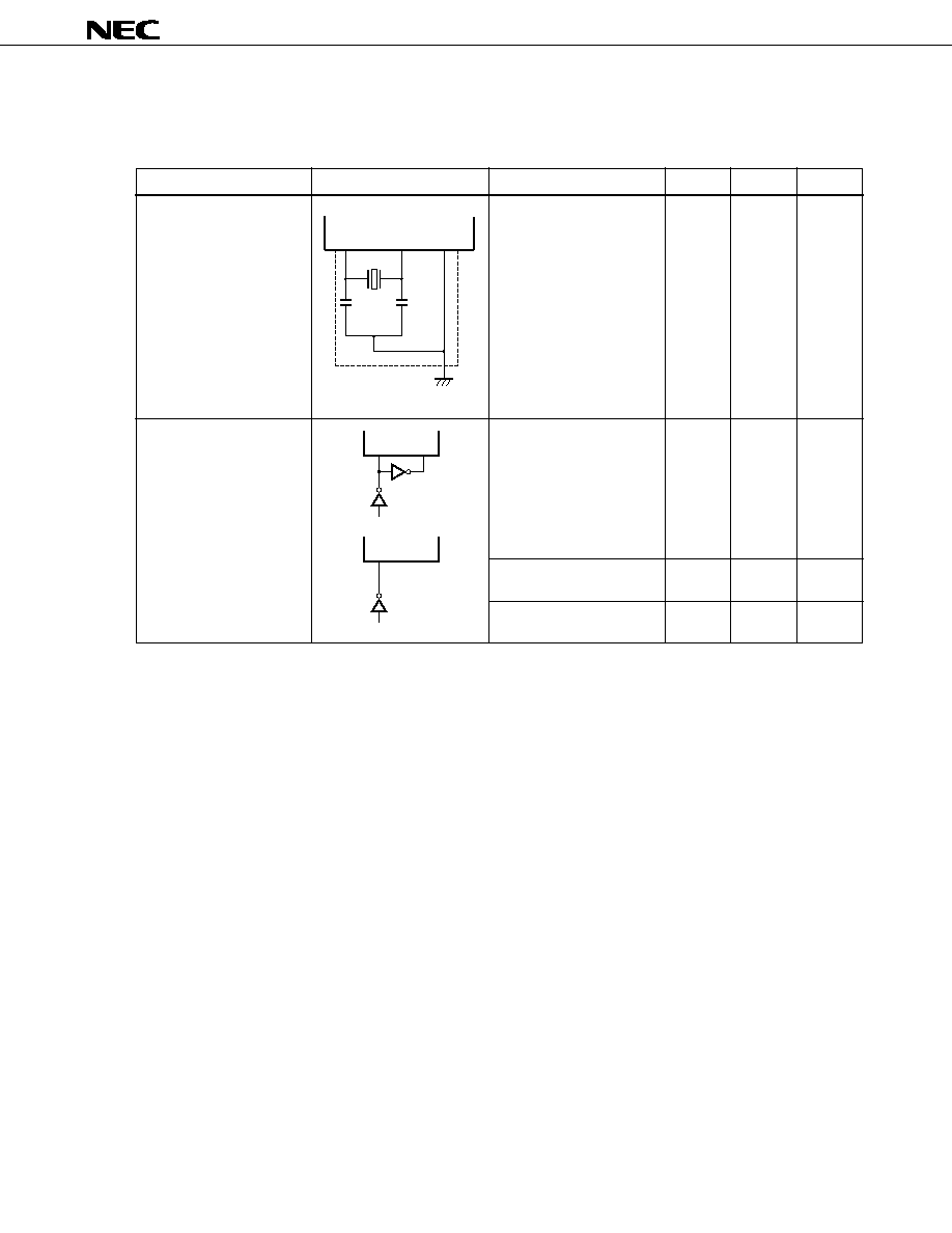
µ
PD78P324, 78P324(A)
43
(3)
µ
PD78P324(A1) Electrical Specifications (3/9)
Oscillator Characteristics (T
A
= ≠40 to +110
∞
C, V
DD
= +5 V
±
10 %, V
SS
= 0 V)
Oscillator
Ceramic oscillator or
crystal oscillator
External clock
Recommended Circuit
Parameter
Oscillation frequency (f
XX
)
X1 input frequency (f
X
)
X1 input rise time, fall time
(t
XR
, t
XF
)
X1 input high-/low-level
width (t
WXH
, t
WXL
)
MIN.
MAX.
Unit
8
12.5
MHz
8
12.5
MHz
0
20
ns
46
100
ns
Caution
When using the system clock oscillation circuit, wire the part encircled in the dotted line in the
following manner to avoid the influence of the wiring capacity, etc.
∑ Make the wiring as short as possible.
∑ Avoid intersecting other signal conductors. Avoid approaching lines in which very high fluctuating
currents run.
∑ Make sure that the grounding point of the oscillation circuit capacitor always has the same
electrical potential as V
SS
. Avoid grounding with a grand pattern in which very high currents run.
∑ Do not fetch signals from the oscillation circuit.
X2
X1
V
SS
C2
C1
X2
X1
X2
X1
HCMOS
inverter
HCMOS
inverter
or
No connection
required
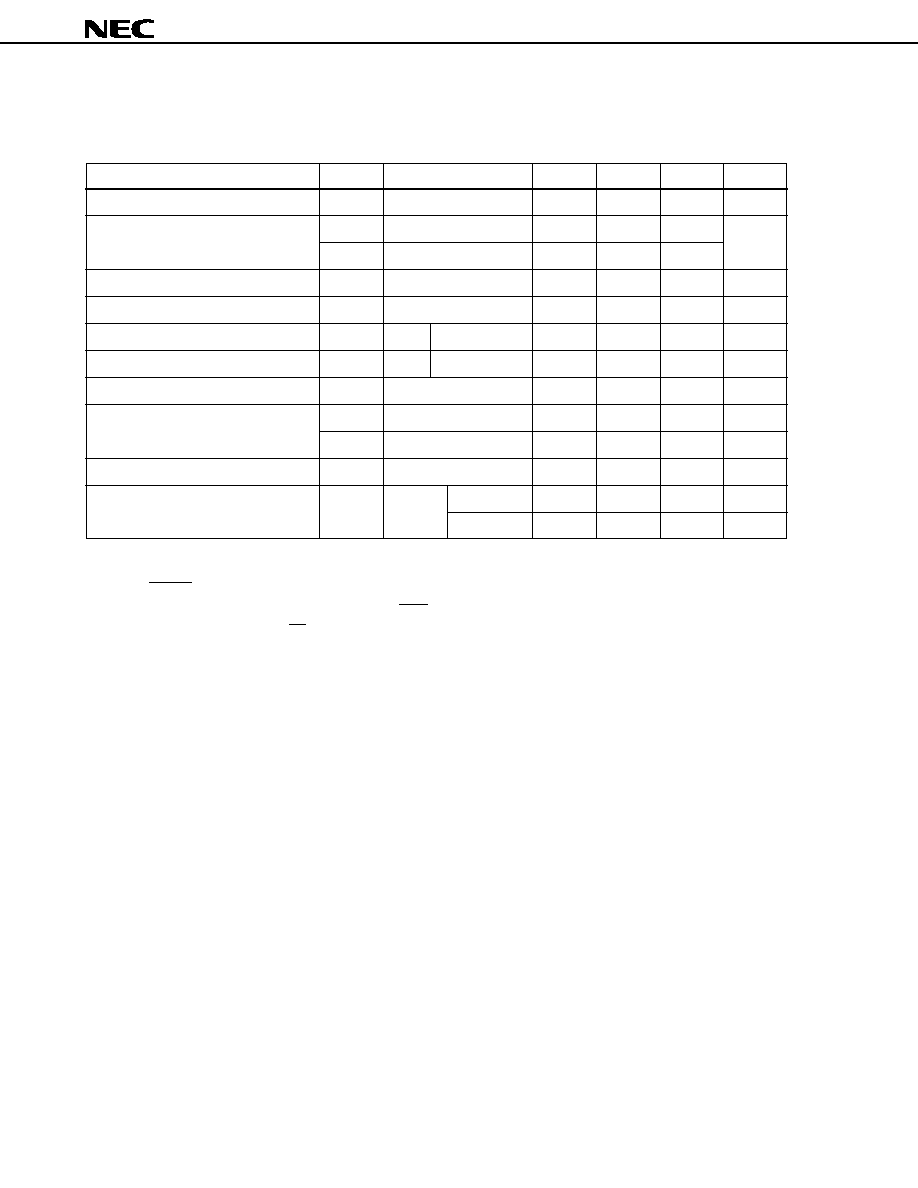
µ
PD78P324, 78P324(A)
44
(3)
µ
PD78P324(A1) Electrical Specifications (4/9)
DC Characteristics (T
A
= ≠40 to +110
∞
C, V
DD
= +5 V
±
10 %, V
SS
= 0 V)
Parameter
Low-level input voltage
High-level input voltage
Low-level output voltage
High-level output voltage
Input leakage current
Analog pin input leakage current
Output leakage current
V
DD
supply current
Data retention voltage
Data retention current
MIN.
TYP.
MAX.
Unit
0
0.8
V
2.2
V
0.8 V
DD
0.45
V
V
DD
≠1.0
V
±
10
µ
A
±
2
µ
A
±
10
µ
A
65
87
mA
25
48
mA
2.5
V
2
100
µ
A
10
1000
µ
A
Symbol
V
IL
V
IH1
V
IH2
V
OL
V
OH
I
LI
I
LIAN
I
LO
I
DD1
I
DD2
V
DDDR
I
DDDR
Condition
Note 1
Note 2
I
OL
= 2.0mA
I
OH
= ≠400
µ
A
Note 3
0 V
V
I
V
DD
Note 4
0 V
V
IAN
AV
REF
0 V
V
O
V
DD
Operation mode
HALT mode
STOP mode
V
DDDR
= 2.5 V
STOP mode
V
DDDR
=5.0 V
±
10%
Notes 1. Pins other than pins in Note 2.
2. RESET, X1, X2, P20/NMI, P21/INTP0, P22/INTP1, P23/INTP2, P24/INTP3, P25/INTP4, P26/INTP5, P27/
INTP6/TI, P32/SO/SB0, P33/SI/SB1, P34/SCK pins.
3. Pins except P20/NMI, EA/V
PP
, X1, X2
4. When not sampling the analog input
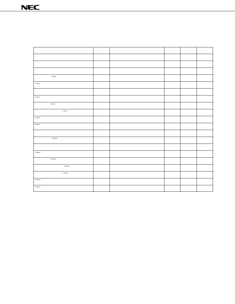
µ
PD78P324, 78P324(A)
45
(3)
µ
PD78P324(A1) Electrical Specifications (5/9)
AC Characteristics (T
A
= ≠40 to +110
∞
C, V
DD
= +5 V
±
10%, V
SS
= 0 V, C
L
= 100pF)
Non-serial Read/Write Operation (when connecting general-purpose memory)
Parameter
Symbol
Condition
MIN.
MAX.
Unit
System clock cycle time
t
CYK
160
250
ns
Address setup time (vs. ASTB
)
t
SAST
40
ns
Address hold time (vs. ASTB
)
t
HSTA
50
ns
Address
RD
delay time
t
DAR
120
ns
RD
address float time
t
FRA
10
ns
Address
data input time
t
DAID
310
ns
RD
data input time
t
DRID
165
ns
ASTB
RD
delay time
t
DSTR
60
ns
Data hold time (vs. RD
)
t
HRID
0
ns
RD
address active time
t
DRA
68
ns
RD low-level width
t
WRL
191
ns
ASTB high-level width
t
WSTH
55
ns
Address
WR
delay time
t
DAW
120
ns
ASTB
data output time
t
DSTOD
120
ns
WR
data output time
t
DWOD
40
ns
ASTB
WR
delay time
t
DSTW
60
ns
Data setup time (vs. WR
)
t
SODW
191
ns
Data hold time (vs. WR
)
t
HWOD
50
ns
WR
ASTB
delay time
t
DWST
60
ns
WR low-level width
t
WWL
195
ns

µ
PD78P324, 78P324(A)
46
(3)
µ
PD78P324(A1) Electrical Specifications (6/9)
t
CYK
-dependent Bus Timing Definition
Symbol
Calculation formula
MIN./MAX.
Unit
t
SAST
0.5T≠40
MIN.
ns
t
HSTA
0.5T≠30
MIN.
ns
t
DAR
T≠40
MIN.
ns
t
DAID
(2.5+n) T≠90
MAX.
ns
t
DRID
(1.5+n) T≠75
MAX.
ns
t
DSTR
0.5T≠20
MIN.
ns
t
DRA
0.5T≠12
MIN.
ns
t
WRL
(1.5+n) T≠49
MIN.
ns
t
WSTH
0.5T≠25
MIN.
ns
t
DAW
T≠40
MIN.
ns
t
DSTOD
0.5T+40
MAX.
ns
t
DSTW
0.5T≠20
MIN.
ns
t
SODW
1.5T≠49
MIN.
ns
t
HWOD
0.5T≠30
MIN.
ns
t
DWST
0.5T≠20
MIN.
ns
t
WWL
(1.5+n) T≠45
MIN.
ns
Remarks
1. T = t
CYK
= 1/f
CLK
(f
CLK
refers to the internal system clock frequency)
2. n refers to the count of weight cycles defined by the user software.
3. Among the parameters for bus timing, only those listed in this table are dependent on t
CYK
.

µ
PD78P324, 78P324(A)
47
(3)
µ
PD78P324(A1) Electrical Specifications (7/9)
Serial Operation (T
A
= ≠40 to +110
∞
C, V
DD
= +5 V
±
10 %, V
SS
= 0 V)
Parameter
Symbol
Condition
MIN.
MAX.
Unit
SCK output
Internal divide-by-eight
1280
µ
s
Serial clock cycle time
t
CYSK
SCK input
External clock
1280
µ
s
SCK output
Internal divide-by-eight
560
ns
Serial clock low-level width
t
WSKL
SCK input
External clock
560
ns
SCK output
Internal divide-by-eight
560
ns
Serial clock high-level width
t
WSKH
SCK input
External clock
560
ns
SI setup time (vs. SCK
)
t
SRXSK
80
ns
SI hold time (vs. SCK
)
t
HSKRX
80
ns
SCK
SO delay time
t
DSKTX
R = 1 k
, C = 100pF
210
ns
t
CYK
-dependent Serial Operation
Symbol
Condition
Calculation Formula
MIN./MAX.
Unit
SCK output
Internal divide-by-eight
8T
MIN.
ns
t
CYSK
SCK input
External clock
8T
MIN.
ns
SCK output
Internal divide-by-eight
4T≠80
MIN.
ns
t
WSKL
SCK input
External clock
4T≠80
MIN.
ns
SCK output
Internal divide-by-eight
4T≠80
MIN.
ns
t
WSKH
SCK input
External clock
4T≠80
MIN.
ns
Remarks
1. T = t
CYK
= 1/f
CLK
(f
CLK
refers to the internal system clock frequency)
2. Among the parameters for serial operation, only those listed in this table are dependent on t
CYK
.
µ
PD78P324, 78P324(A)
48
(3)
µ
PD78P324(A1) Electrical Specifications (8/9)
Other Operations (T
A
= ≠40 to +110
∞
C, V
DD
= +5 V
±
10 %, V
DD
= 0 V)
Parameter
Symbol
Condition
MIN.
MAX.
Unit
NMI high-/low-level width
t
WNIH
, t
WNIL
Analog noises removed
4
µ
s
INTP0 high-/low-level width
t
WIOH
, t
WIOL
1280
ns
INTP1 high-/low-level width
t
WI1H
, t
WI1L
1280
ns
INTP2 high-/low-level width
t
WI2H
, t
WI2L
1280
ns
INTP3 high-/low-level width
t
WI3H
, t
WI3L
1280
ns
INTP4 high-/low-level width
t
WI4H
, t
WI4L
1280
ns
INTP5 high-/low-level width
t
WI5H
, t
WI5L
1280
ns
INTP6 high-/low-level width
t
WI6H
, t
WI6L
1280
ns
RESET high-/low-level width
t
WRSH
, t
WRSL
Analog noises removed
3.5
µ
s
TI high-/low-level width
t
WTIH
, t
WTIL
1280
ns
V
DD
rise/fall time
t
RVD
, t
FVD
200
µ
s
Other t
CYK
-dependent Operations
Symbol
Calculation formula
MIN./MAX.
Unit
t
WIOH
8T
MIN.
ns
t
WIOL
8T
MIN.
ns
t
WI1H
8T
MIN.
ns
t
WI1L
8T
MIN.
ns
t
WI2H
8T
MIN.
ns
t
WI2L
8T
MIN.
ns
t
WI3H
8T
MIN.
ns
t
WI3L
8T
MIN.
ns
t
WI4H
8T
MIN.
ns
t
WI4L
8T
MIN.
ns
t
WI5H
8T
MIN.
ns
t
WI5L
8T
MIN.
ns
t
WI6H
8T
MIN.
ns
t
WI6L
8T
MIN.
ns
t
WTIH
8T
MIN.
ns
t
WTIL
8T
MIN.
ns
Remarks
1. T = t
CYK
= 1/f
CLK
(f
CLK
refers to the internal system clock frequency)
2. Only the parameters listed in this table depend on t
CYK
.

µ
PD78P324, 78P324(A)
49
(3)
µ
PD78P324(A1) Electrical Specifications (9/9)
AC Timing Test Point
A/D Converter Characteristics (T
A
= ≠40 to +110
∞
C, V
DD
= +5 V
±
10 %, V
SS
= AV
SS
= 0 V, V
DD
≠0.5 V
AV
DD
V
DD
)
Parameter
Resolution
Total error
Note 1
Quantization error
Conversion time
Sampling time
Zero-scale error
Note 1
Full-scale error
Note 1
Non-linear error
Note 1
Analog input voltage
Note 2
Analog input impedance
Reference voltage
AV
REF
current
AV
DD
supply current
A/D converter data retention current
MIN.
TYP.
MAX.
Unit
10
bit
±
0.4
%FSR
±
0.7
%FSR
±
1/2
LSB
144
t
CYK
24
t
CYK
±
1.5
±
2.5
LSB
±
1.5
±
4.5
LSB
±
1.5
±
2.5
LSB
±
1.5
±
4.5
LSB
±
1.5
±
2.5
LSB
±
1.5
±
4.5
LSB
0
AV
DD
V
10
M
Note 3
3.4
AV
DD
V
1.0
3.0
mA
2.0
6.0
mA
2
100
µ
A
10
1000
µ
A
Symbol
t
CONV
t
SAMP
V
IAN
R
AN
AV
REF
AI
REF
AI
DD
AI
DDDR
Condition
4.5 V
AV
REF
AV
DD
3.5 V
AV
REF
AV
DD
4.5 V
AV
REF
AV
DD
3.4 V
AV
REF
AV
DD
4.5 V
AV
REF
AV
DD
3.4 V
AV
REF
AV
DD
4.5 V
AV
REF
AV
DD
3.4 V
AV
REF
AV
DD
When not sampled
When sampled
Operation mode
AV
DDDR
= 2.5 V
STOP mode
AV
DDDR
=5 V
±
10%
Notes 1. Quantization error excluded.
2. When V
IAN
= 0 V, the conversion result becomes 000H.
When 0 V < V
IAN
< AV
REF
, the conversion is performed at a resolution of 10 bits.
When AV
REF
V
IAN
AV
DD
, the conversion result is 3FFH.
3. The analog input impedance in sampling is the same as the equivalent circuit shown in the diagram
below. (The values in the diagram are TYP. values; therefore, they are not assured.)
0.8V
DD
or 2.2V
0.8V
0.8V
DD
or 2.2V
0.8V
Test point
V
DD
0V
20k
10pF
30pF
Analog input pin
( input
capacitance
included )
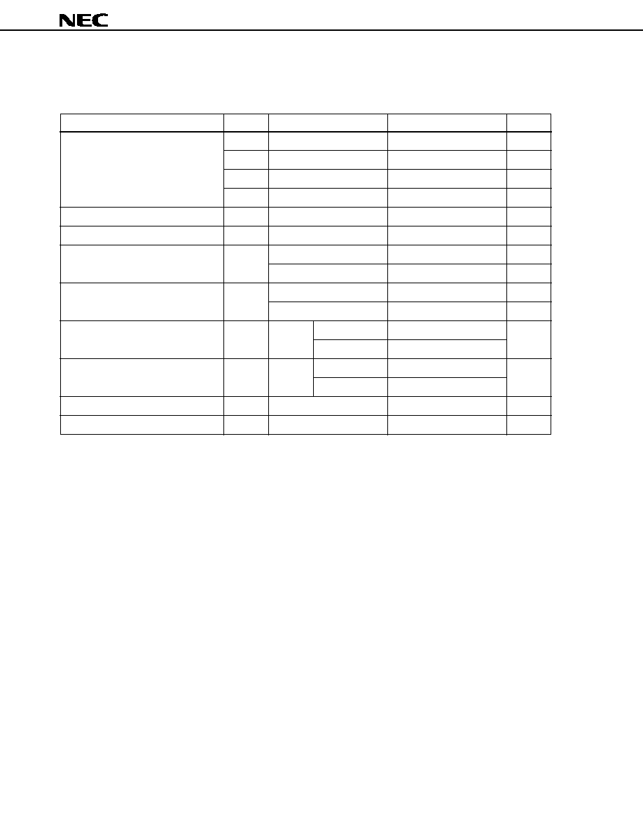
µ
PD78P324, 78P324(A)
50
(4)
µ
PD78P324(A2) Electrical Specifications (1/9)
Absolute Maximum Ratings (T
A
= 25
∞
C)
Parameter
Supply voltage
Input voltage
Output voltage
Low-level output current
High-level output current
Analog input voltage
A/D converter reference input voltage
Operating ambient temperature
Storage temperature
Unit
V
V
V
V
V
V
mA
mA
mA
mA
V
V
∞
C
∞
C
Rating
≠0.5 to +7.0
≠0.5 to V
DD
+0.5
≠0.5 to +13.5
≠0.5 to +0.5
≠0.5 to V
DD
+0.5
≠0.5 to V
DD
+0.5
4.0
90
≠1.0
≠20
≠0.5 to V
DD
+0.5
≠0.5 to AV
DD
+0.5
≠0.5 to V
DD
+0.5
≠0.5 to AV
DD
+0.5
≠40 to +125
≠65 to +150
Symbol
V
DD
AV
DD
V
PP
AV
SS
V
I
V
O
I
OL
I
OH
V
IAN
AV
REF
T
A
T
stg
Condition
Notes 1, 2
All output pins
Total of all output pins
All output pins
Total of all output pins
AV
DD
> V
DD
Notes 2, 3
V
DD
AV
DD
AV
DD
> V
DD
V
DD
AV
DD
Notes 1. Except P70/AN0-P77/AN7.
2. The overvoltage condition of the allowable pin injectioncurrent characteristics in overvoltage application
is excluded.
3. P70/AN0-P77/AN7 pins.
Caution
If the absolute maximum rating of any one of the parameters is exceeded even momentarily, the
quality of the product may be degraded. In other words, the product may be physically damaged
if any of the absolute maximum ratings is exceeded. Be sure to use the product without exceeding
these ratings.
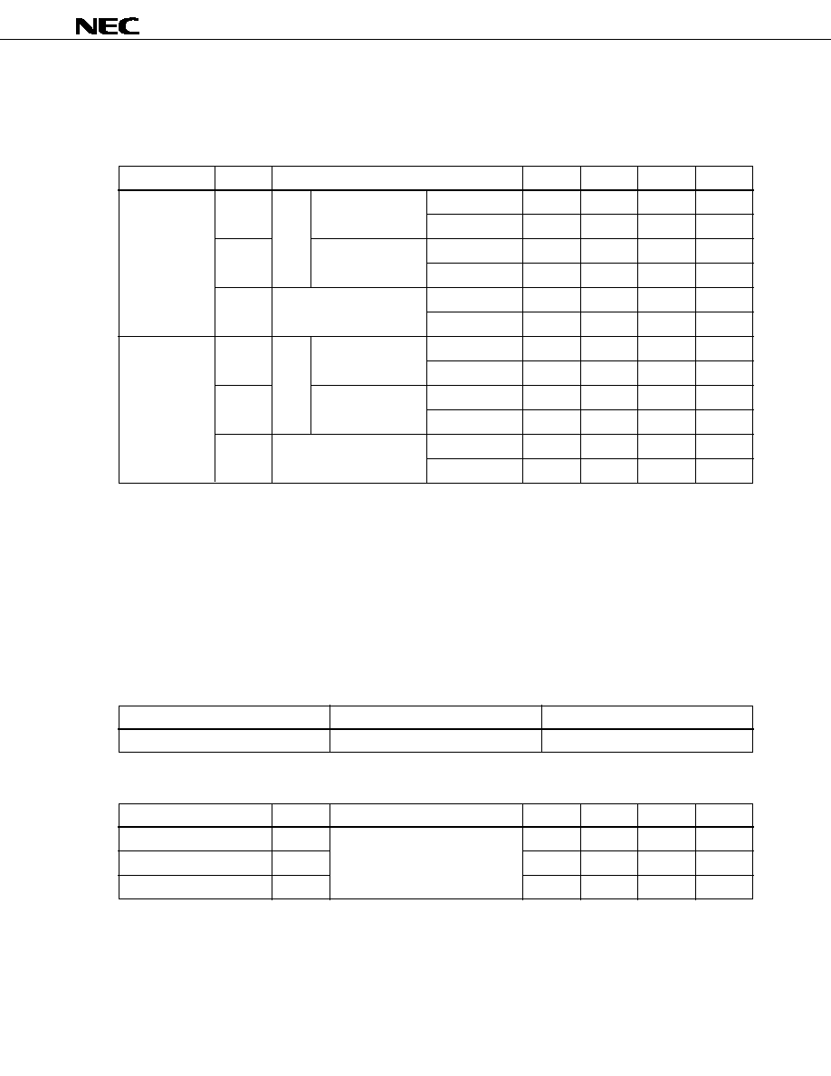
µ
PD78P324, 78P324(A)
51
(4)
µ
PD78P324(A2) Electrical Specifications (2/9)
Permissible Pin Injection Current Characteristics in Overvoltage Application (T
A
= ≠40 to +125
∞
C, V
DD
= +5 V
±
10%, V
SS
= 0 V)
Parameter
Positive
injection
current
(V
IN
> V
DD
)
Negative
injection
current
(V
IN
< V
SS
)
Symbol
I
IJH1
I
IJH2
I
IJH
I
IJL1
I
IJL2
I
IJL
MIN.
TYP.
MAX.
Unit
10
mA
0.5
mA
3
mA
1
mA
100
mA
5
mA
≠4
mA
≠0.4
mA
≠4
mA
≠0.3
mA
≠40
mA
≠3
mA
Condition
Peak value
Mean value
1 pin
Peak value
Mean value
Peak value
Total of all input pins
Mean value
Peak value
Mean value
1 pin
Peak value
Mean value
Peak value
Total of all input pins
Mean value
Input ports other
than ANn (n = 0-7)
ANn (n = 0-7)
Input ports other
than ANn (n = 0-7)
ANn (n = 0-7)
Cautions. 1. When the injection current has run into the analog input pin (ANn: n = 0-7), the A/D conversion
result of the analog input contiguous to the current injection pin has the value of the standard
in which the injection current is not running plus
±
2LSB.
2. The mean value (absolute value) of the pin injected current is as follows:
Mean value = ((1/T)
| i(t) |
3/2
dt)
2/3
In this, i(t) refers to the pin injected current. The maximum value of |i(t)| is the peak value.
Recommended Operating Range
Oscillation Frequency
T
A
V
DD
8MHz
f
XX
12.5 MHz
≠40 to +125
∞
C
+5.0 V
±
10 %
Capacitance (T
A
= 25
∞
C, V
SS
= V
DD
= 0 V)
Parameter
Input capacitance
Output capacitance
I/O capacitance
Symbol
C
I
C
O
C
IO
Condition
f = 1 MHz;
0 V except measured pins
MIN.
TUP.
MAX.
Unit
10
pF
20
pF
20
pF
T
0

µ
PD78P324, 78P324(A)
52
(4)
µ
PD78P324(A2) Electrical Specifications (3/9)
Oscillator Characteristics (T
A
= 40 to +125
∞
C, V
DD
= +5 V
±
10 %, V
SS
= 0 V)
Oscillator
Ceramic oscillator or
crystal oscillator
External clock
Recommended Circuit
Parameter
Oscillation frequency (f
XX
)
X1 input frequency (f
X
)
X1 input rise time, fall time
(t
XR
, t
XF
)
X1 input high-/low-level
width (t
WXH
, t
WXL
)
MIN.
MAX.
Unit
8
12.5
MHz
8
12.5
MHz
0
20
ns
46
100
ns
Caution
When using the system clock oscillation circuit, wire the part encircled in the dotted line in the
following manner to avoid the influence of the wiring capacity, etc.
∑ Make the wiring as short as possible.
∑ Avoid intersecting other signal conductors. Avoid approaching lines in which very high fluctuating
currents run.
∑ Make sure that the grounding point of the oscillation circuit capacitor always has the same
electrical potential as V
SS
. Avoid grounding with a grand pattern in which very high currents run.
∑ Do not fetch signals from the oscillation circuit.
X2
X1
V
SS
C2
C1
X2
X1
X2
X1
HCMOS
inverter
HCMOS
inverter
or
No connection
required
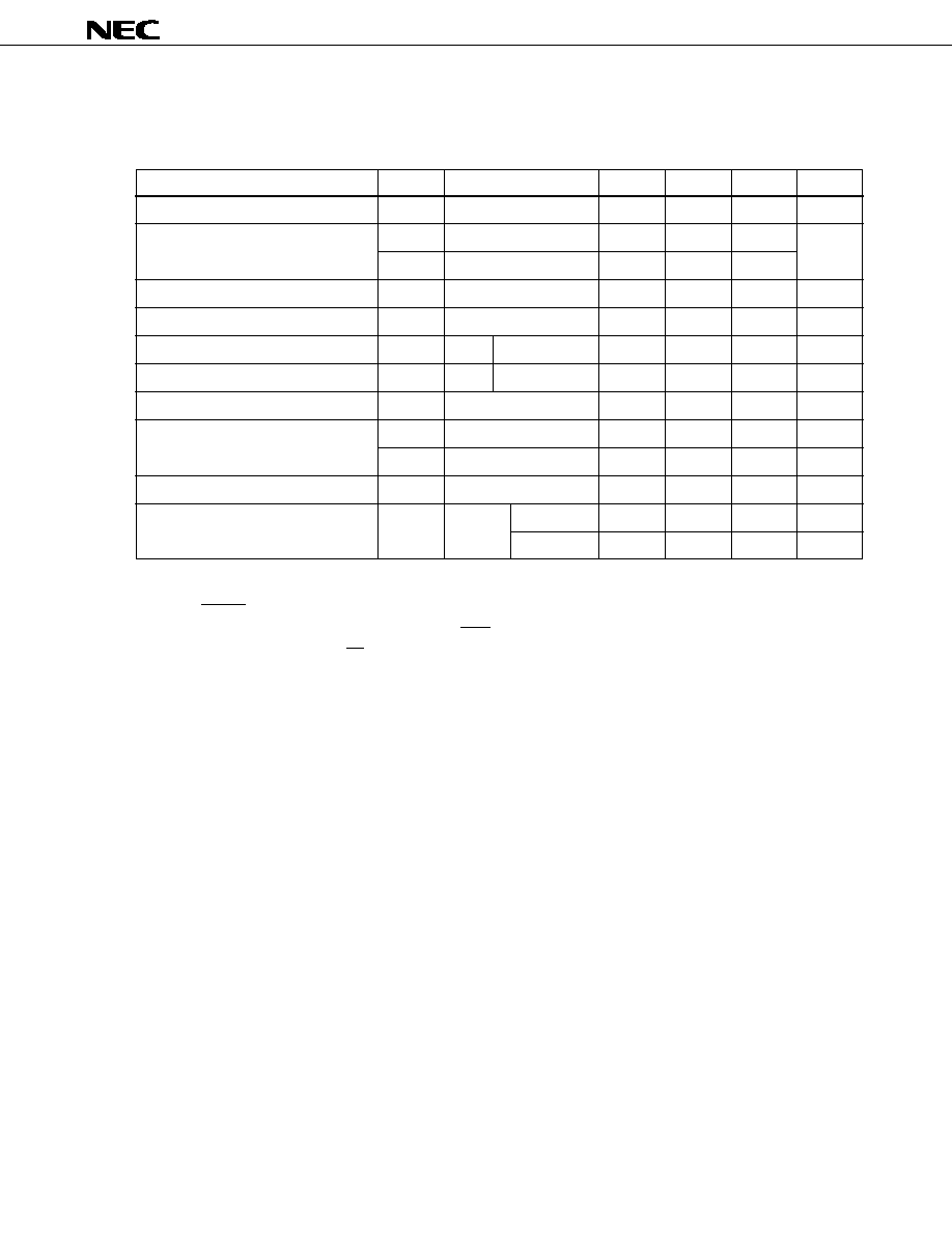
µ
PD78P324, 78P324(A)
53
(4)
µ
PD78P324(A2) Electrical Specifications (4/9)
DC Characteristics (T
A
= ≠40 to +125
∞
C, V
DD
= +5 V
±
10 %, V
SS
= 0 V)
Parameter
Low-level input voltage
High-level input voltage
Low-level output voltage
High-level output voltage
Input leakage current
Analog pin input leakage current
Output leakage current
V
DD
supply current
Data retention voltage
Data retention current
MIN.
TYP.
MAX.
Unit
0
0.8
V
2.2
V
0.8 V
DD
0.45
V
V
DD
≠1.0
V
±
10
µ
A
±
2
µ
A
±
10
µ
A
65
87
mA
25
48
mA
2.5
V
2
100
µ
A
10
1000
µ
A
Symbol
V
IL
V
IH1
V
IH2
V
OL
V
OH
I
LI
I
LIAN
I
LO
I
DD1
I
DD2
V
DDDR
I
DDDR
Condition
Note 1
Note 2
I
OL
= 2.0mA
I
OH
= ≠400
µ
A
Note 3
0 V
V
I
V
DD
Note 4
0 V
V
IAN
AV
REF
0 V
V
O
V
DD
Operation mode
HALT mode
STOP mode
V
DDDR
= 2.5 V
STOP mode
V
DDDR
=5.0 V
±
10%
Notes 1. Pins other than pins in Note 2.
2. RESET, X1, X2, P20/NMI, P21/INTP0, P22/INTP1, P23/INTP2, P24/INTP3, P25/INTP4, P26/INTP5, P27/
INTP6/TI, P32/SO/SB0, P33/SI/SB1, P34/SCK pins.
3. Pins except P20/NMI, EA/V
PP
, X1, X2
4. When not sampling the analog input
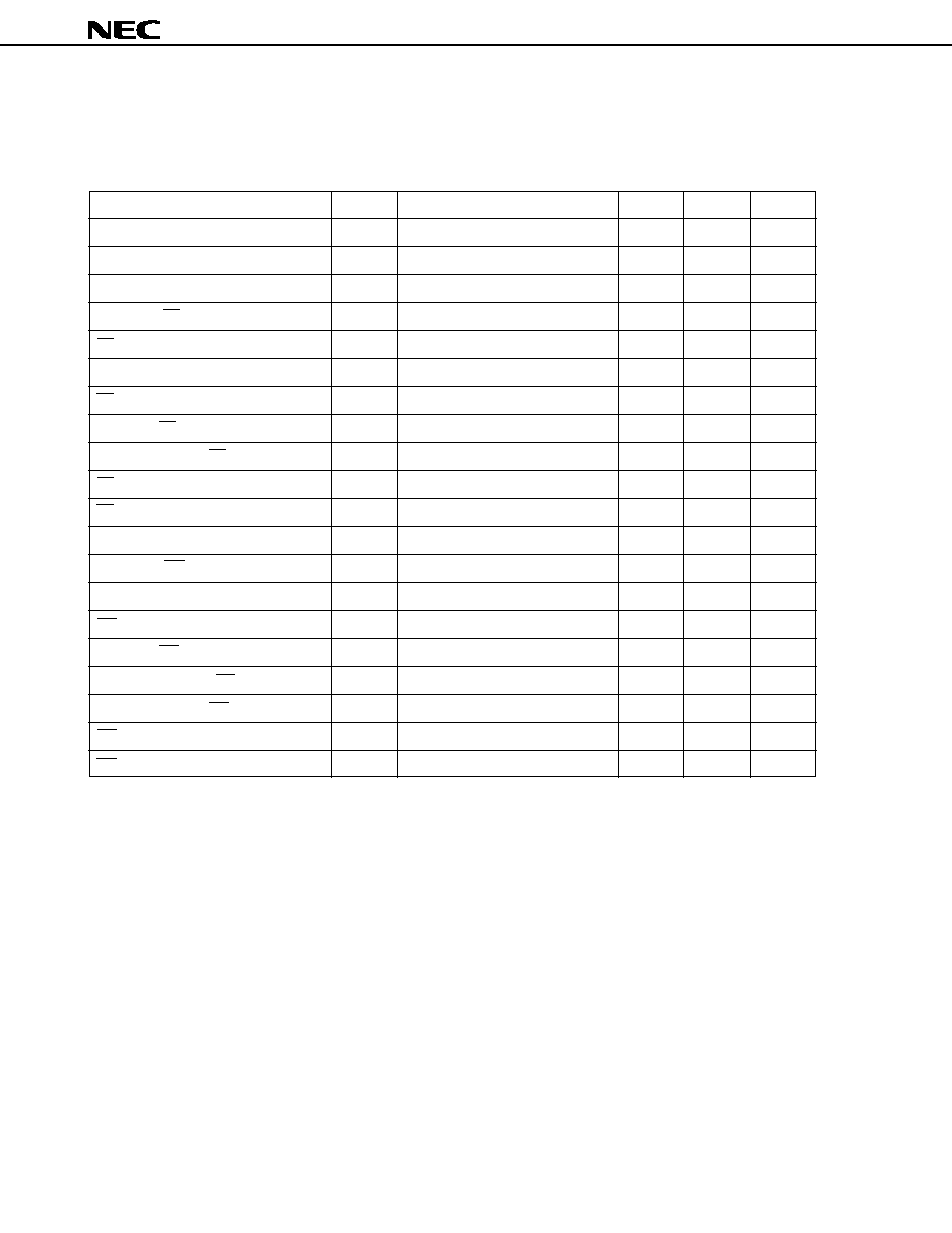
µ
PD78P324, 78P324(A)
54
(4)
µ
PD78P324(A2) Electrical Specifications (5/9)
AC Characteristics (T
A
= ≠40 to +125
∞
C, V
DD
= +5 V
±
10%, V
SS
= 0 V, C
L
= 100pF)
Non-serial Read/Write Operation (when connecting general-purpose memory)
Parameter
Symbol
Condition
MIN.
MAX.
Unit
System clock cycle time
t
CYK
160
250
ns
Address setup time (vs. ASTB
)
t
SAST
40
ns
Address hold time (vs. ASTB
)
t
HSTA
50
ns
Address
RD
delay time
t
DAR
120
ns
RD
address float time
t
FRA
10
ns
Address
data input time
t
DAID
310
ns
RD
data input time
t
DRID
165
ns
ASTB
RD
delay time
t
DSTR
60
ns
Data hold time (vs. RD
)
t
HRID
0
ns
RD
address active time
t
DRA
68
ns
RD low-level width
t
WRL
191
ns
ASTB high-level width
t
WSTH
55
ns
Address
WR
delay time
t
DAW
120
ns
ASTB
data output time
t
DSTOD
120
ns
WR
data output time
t
DWOD
40
ns
ASTB
WR
delay time
t
DSTW
60
ns
Data setup time (vs. WR
)
t
SODW
191
ns
Data hold time (vs. WR
)
t
HWOD
50
ns
WR
ASTB
delay time
t
DWST
60
ns
WR low-level width
t
WWL
195
ns

µ
PD78P324, 78P324(A)
55
(4)
µ
PD78P324(A2) Electrical Specifications (6/9)
t
CYK
-dependent Bus Timing Definition
Symbol
Calculation formula
MIN./MAX.
Unit
t
SAST
0.5T≠40
MIN.
ns
t
HSTA
0.5T≠30
MIN.
ns
t
DAR
T≠40
MIN.
ns
t
DAID
(2.5+n) T≠90
MAX.
ns
t
DRID
(1.5+n) T≠75
MAX.
ns
t
DSTR
0.5T≠20
MIN.
ns
t
DRA
0.5T≠12
MIN.
ns
t
WRL
(1.5+n) T≠49
MIN.
ns
t
WSTH
0.5T≠25
MIN.
ns
t
DAW
T≠40
MIN.
ns
t
DSTOD
0.5T+40
MAX.
ns
t
DSTW
0.5T≠20
MIN.
ns
t
SODW
1.5T≠49
MIN.
ns
t
HWOD
0.5T≠30
MIN.
ns
t
DWST
0.5T≠20
MIN.
ns
t
WWL
(1.5+n) T≠45
MIN.
ns
Remarks
1. T = t
CYK
= 1/f
CLK
(f
CLK
refers to the internal system clock frequency)
2. n refers to the count of weight cycles defined by the user software.
3. Among the parameters for bus timing, only those listed in this table are dependent on t
CYK
.
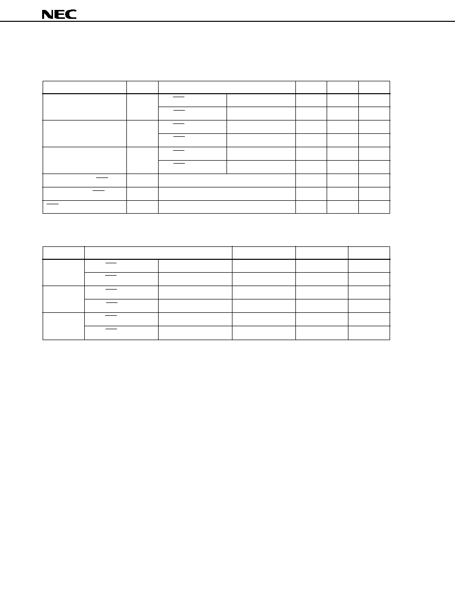
µ
PD78P324, 78P324(A)
56
(4)
µ
PD78P324(A2) Electrical Specifications (7/9)
Serial Operation (T
A
= 40 to +125
∞
C, V
DD
= +5 V
±
10 %, V
SS
= 0 V)
Parameter
Symbol
Condition
MIN.
MAX.
Unit
SCK output
Internal divide-by-eight
1280
µ
s
Serial clock cycle time
t
CYSK
SCK input
External clock
1280
µ
s
SCK output
Internal divide-by-eight
560
ns
Serial clock low-level width
t
WSKL
SCK input
External clock
560
ns
SCK output
Internal divide-by-eight
560
ns
Serial clock high-level width
t
WSKH
SCK input
External clock
560
ns
SI setup time (vs. SCK
)
t
SRXSK
80
ns
SI hold time (vs. SCK
)
t
HSKRX
80
ns
SCK
SO delay time
t
DSKTX
R = 1 k
, C = 100pF
210
ns
t
CYK
-dependent Serial Operation
Symbol
Condition
Calculation Formula
MIN./MAX.
Unit
SCK output
Internal divide-by-eight
8T
MIN.
ns
t
CYSK
SCK input
External clock
8T
MIN.
ns
SCK output
Internal divide-by-eight
4T≠80
MIN.
ns
t
WSKL
SCK input
External clock
4T≠80
MIN.
ns
SCK output
Internal divide-by-eight
4T≠80
MIN.
ns
t
WSKH
SCK input
External clock
4T≠80
MIN.
ns
Remarks
1. T = t
CYK
= 1/f
CLK
(f
CLK
refers to the internal system clock frequency)
2. Among the parameters for serial operation, only those listed in this table are dependent on t
CYK
.

µ
PD78P324, 78P324(A)
57
(4)
µ
PD78P324(A2) Electrical Specifications (8/9)
Other Operations (T
A
= ≠40 to +125
∞
C, V
DD
= +5 V
±
10 %, V
DD
= 0 V)
Parameter
Symbol
Condition
MIN.
MAX.
Unit
NMI high-/low-level width
t
WNIH
, t
WNIL
Analog noises removed
4
µ
s
INTP0 high-/low-level width
t
WIOH
, t
WIOL
1280
ns
INTP1 high-/low-level width
t
WI1H
, t
WI1L
1280
ns
INTP2 high-/low-level width
t
WI2H
, t
WI2L
1280
ns
INTP3 high-/low-level width
t
WI3H
, t
WI3L
1280
ns
INTP4 high-/low-level width
t
WI4H
, t
WI4L
1280
ns
INTP5 high-/low-level width
t
WI5H
, t
WI5L
1280
ns
INTP6 high-/low-level width
t
WI6H
, t
WI6L
1280
ns
RESET high-/low-level width
t
WRSH
, t
WRSL
Analog noises removed
3.5
µ
s
TI high-/low-level width
t
WTIH
, t
WTIL
1280
ns
V
DD
rise/fall time
t
RVD
, t
FVD
200
µ
s
Other t
CYK
-dependent Operations
Symbol
Calculation formula
MIN./MAX.
Unit
t
WIOH
8T
MIN.
ns
t
WIOL
8T
MIN.
ns
t
WI1H
8T
MIN.
ns
t
WI1L
8T
MIN.
ns
t
WI2H
8T
MIN.
ns
t
WI2L
8T
MIN.
ns
t
WI3H
8T
MIN.
ns
t
WI3L
8T
MIN.
ns
t
WI4H
8T
MIN.
ns
t
WI4L
8T
MIN.
ns
t
WI5H
8T
MIN.
ns
t
WI5L
8T
MIN.
ns
t
WI6H
8T
MIN.
ns
t
WI6L
8T
MIN.
ns
t
WTIH
8T
MIN.
ns
t
WTIL
8T
MIN.
ns
Remarks
1. T = t
CYK
= 1/f
CLK
(f
CLK
refers to the internal system clock frequency)
2. Only the parameters listed in this table depend on t
CYK
.

µ
PD78P324, 78P324(A)
58
(4)
µ
PD78P324(A2) Electrical Specifications (9/9)
AC Timing Test Point
A/D Converter Characteristics (T
A
= ≠40 to +125
∞
C, V
DD
= +5 V
±
10 %, V
SS
= AV
SS
= 0 V, V
DD
≠0.5 V
AV
DD
V
DD
)
Parameter
Resolution
Total error
Note 1
Quantization error
Conversion time
Sampling time
Zero-scale error
Note 1
Full-scale error
Note 1
Non-linear error
Note 1
Analog input voltage
Note 2
Analog input impedance
Reference voltage
AV
REF
current
AV
DD
supply current
A/D converter data retention current
MIN.
TYP.
MAX.
Unit
10
bit
±
0.4
%FSR
±
0.7
%FSR
±
1/2
LSB
144
t
CYK
24
t
CYK
±
1.5
±
2.5
LSB
±
1.5
±
4.5
LSB
±
1.5
±
2.5
LSB
±
1.5
±
4.5
LSB
±
1.5
±
2.5
LSB
±
1.5
±
4.5
LSB
0
AV
DD
V
10
M
Note 3
3.4
AV
DD
V
1.0
3.0
mA
2.0
6.0
mA
2
100
µ
A
10
1000
µ
A
Symbol
t
CONV
t
SAMP
V
IAN
R
AN
AV
REF
AI
REF
AI
DD
AI
DDDR
Condition
4.5 V
AV
REF
AV
DD
3.5 V
AV
REF
AV
DD
4.5 V
AV
REF
AV
DD
3.4 V
AV
REF
AV
DD
4.5 V
AV
REF
AV
DD
3.4 V
AV
REF
AV
DD
4.5 V
AV
REF
AV
DD
3.4 V
AV
REF
AV
DD
When not sampled
When sampled
Operation mode
AV
DDDR
= 2.5 V
STOP mode
AV
DDDR
=5 V
±
10%
Notes 1. Quantization error excluded.
2. When V
IAN
= 0 V, the conversion result becomes 000H.
When 0 V < V
IAN
< AV
REF
, the conversion is performed at a resolution of 10 bits.
When AV
REF
V
IAN
AV
DD
, the conversion result is 3FFH.
3. The analog input impedance in sampling is the same as the equivalent circuit shown in the diagram
below. (The values in the diagram are TYP. values; therefore, they are not assured.)
0.8V
DD
or 2.2V
0.8V
0.8V
DD
or 2.2V
0.8V
Test point
V
DD
0V
20k
10pF
30pF
Analog input pin
( input
capacitance
included )

µ
PD78P324, 78P324(A)
59
Non-serial Read Operation
Non-serial Write Operation
(CLK)
P50-P57
(Output)
Hi-Z
Hi-Z
Hi-Z
Hi-Z
P40-P47
(Input/Output)
ASTB
(Output)
Data (Input)
Lower address(Output)
Lower address(Output)
Upper address
RD
(Output)
(CLK)
P50-P57
(Output)
P40-P47
(Input/Output)
ASTB
(Output)
WR
(Output)
Upper address
Upper address
Upper address
Undfined
Lower address(Output)
Data (Output)
Lower address(Output)
t
WSTH
t
DAID
t
SAST
t
HSTA
t
HRID
t
FRA
t
DSTR
t
DAR
t
CYK
t
DRA
t
DRID
t
WRL
t
SAST
t
WSTH
t
HSTA
t
DSTOD
t
DSTW
t
DAW
t
DWOD
t
SODW
t
HWOD
t
DWST
t
WWL
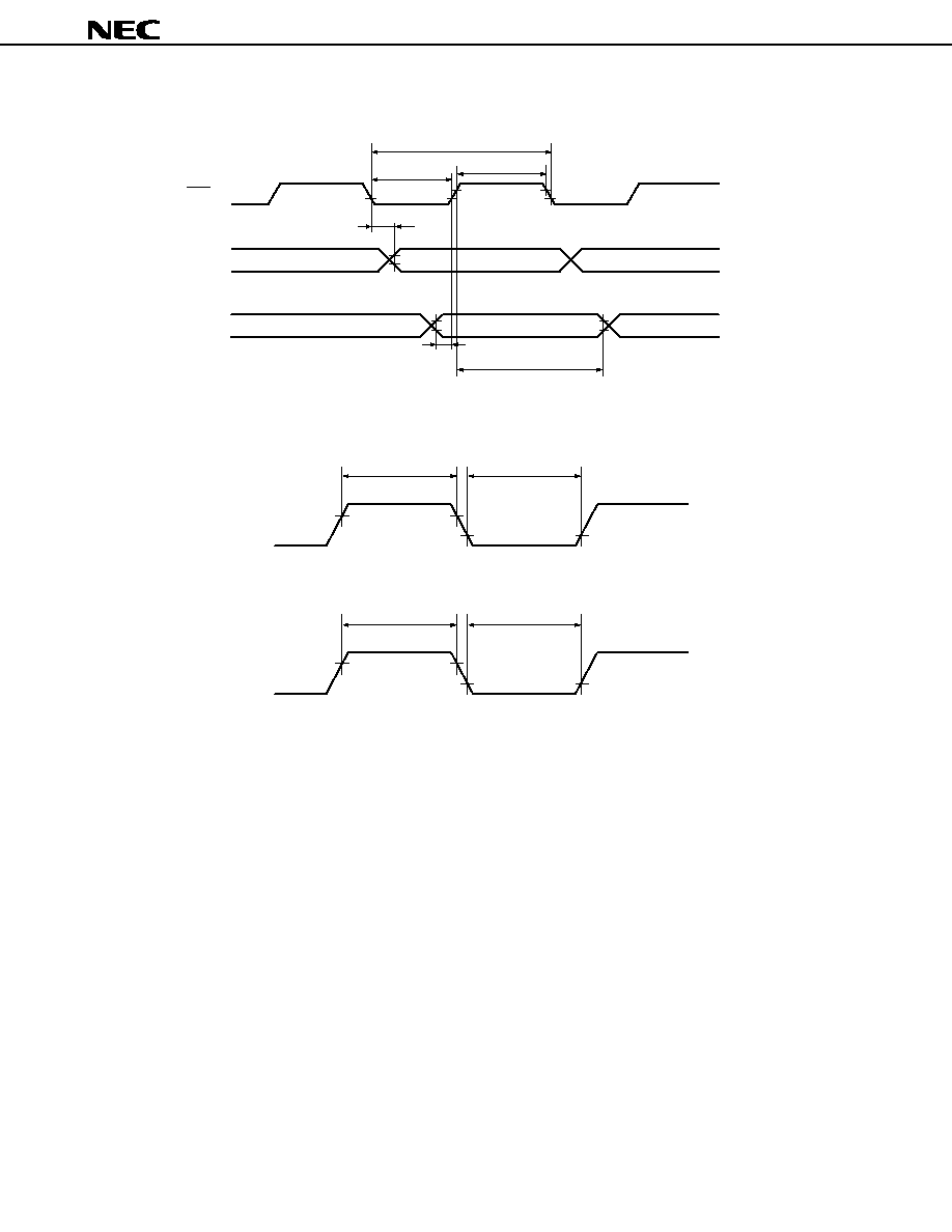
µ
PD78P324, 78P324(A)
60
Serial Operation
Interrupt Input Timing
Remark
n = 0-6
NMI
1NTPn
SCK
SO
SI
t
WNIH
t
WNIL
t
WInH
t
WInL
0.8V
DD
0.8V
t
HSKRX
t
SRXSK
t
DSKTX
t
WSKL
t
WSKH
t
CYSK

µ
PD78P324, 78P324(A)
61
Reset Input Timing
TI Pin Input Timing
Data Retention Timing
t
WRSH
t
WRSL
t
WTIH
t
WTIL
0.8V
DD
0.8V
RESET
TI
V
DD
90%
V
DDDR
10%
t
FVD
t
RVD
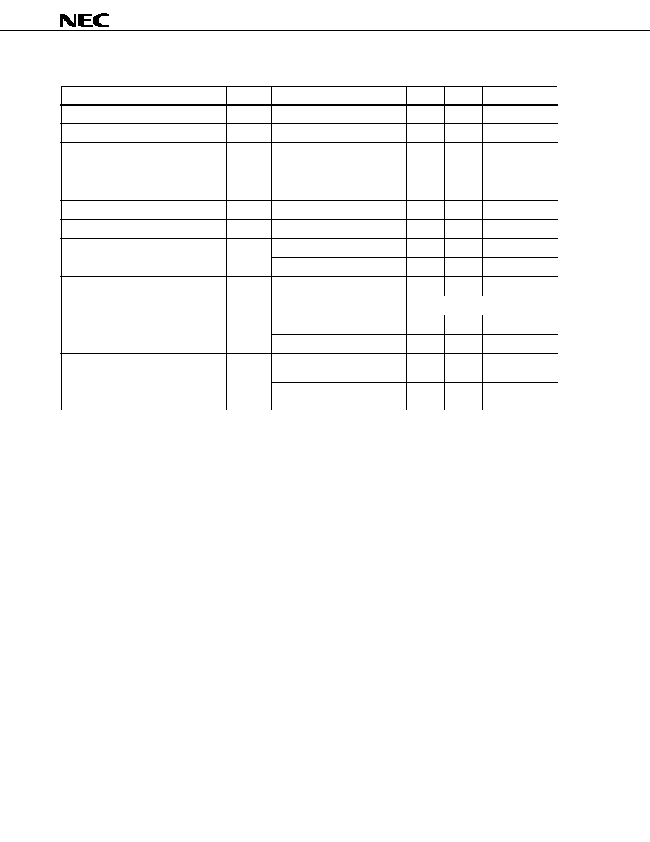
µ
PD78P324, 78P324(A)
62
Parameter
High-level input voltage
Low-level input voltage
Input leakage current
High-level output voltage
Low-level output voltage
Input current
Output leakage current
V
DDP
supply voltage
V
PP
supply voltage
V
DDP
supply current
V
PP
supply current
Symbol
Note 1
V
IH
V
IL
I
LI
V
OH
V
OL
--
--
V
CC
V
PP
I
DD
I
PP
Condition
0
V
I
V
DDP
Note 2
I
OH
= ≠400
µ
A
I
OL
= 2.0
µ
A
A9(P20/NMI) pin, 0
V
O
V
DDP
0
V
O
V
DDP
, OE = V
IH
Program memory Write mode
Program memory Read mode
Program memory Write mode
Program memory Read mode
Program memory Write mode
Program memory Read mode
Program memory Write mode
CE = PGM
Program memory Read mode
V
PP
= V
DD
DC Programming Characteristics (T
A
= 25
±
5
∞
C, V
SS
= 0 V)
MIN.
TYP.
MAX.
Unit
2.4
V
DDP
+0.3
V
≠0.3
0.8
V
±
10
µ
A
2.4
V
0.45
V
±
10
µ
A
±
10
µ
A
6.25
65
6.75
V
4.5
5.0
5.5
V
12.2
12.5
12.8
V
V
PP
= V
DDP
V
30
mA
50
mA
50
mA
1
100
µ
A
Notes 1. Refers to the symbol of the corresponding
µ
PD27C1001A.
2. V
DDP
refers to the V
DD
pin in programming.
Symbol
V
IH
V
IL
I
LI
V
OH
V
OL
I
A9
I
LO
V
DDP
V
PP
I
DD
I
PP
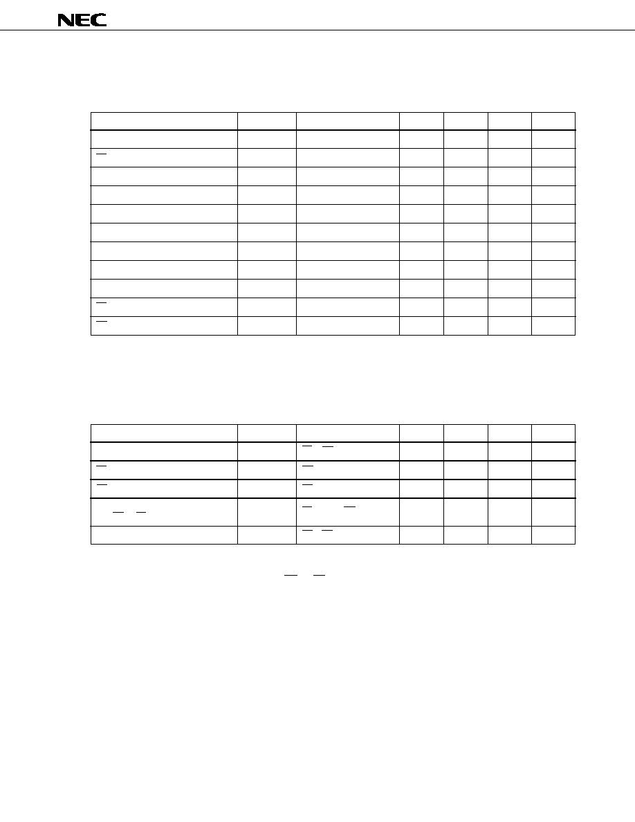
µ
PD78P324, 78P324(A)
63
AC Programming Characteristics (T
A
= 25
±
5
∞
C, V
SS
= 0 V)
In PROM Write Mode
Parameter
Address setup time
CE set time
Input data setup time
Address hold time
Input data hold time
Output data hold time
V
PP
setup time
V
DDP
setup time
Initial program pulse width
OE set time
OE
valid data delay time
MIN.
TYP.
MAX.
Unit
2
µ
s
2
µ
s
2
µ
s
2
µ
s
2
µ
s
0
130
ns
2
µ
s
2
µ
s
0.095
0.1
0.105
ms
2
µ
s
200
ns
Symbol
Note1
t
AS
t
CES
t
DS
t
AH
t
DH
t
DF
t
VPS
t
VDS
Note 2
t
PW
t
OES
t
OE
Condition
Notes 1. Corresponds to the symbol of
µ
PD27C1001A (t
VDS
excluded).
2. The symbol of t
VDS
on
µ
PD27C1001A is t
VCS
.
In PROM Read Mode
Parameter
Address
data output time
CE
data output time
OE
data output time
Data hold time
(vs. OE
, CE
)
Note 2
Data hold time (vs. address)
MIN.
TYP.
MAX.
Unit
2
µ
s
1
µ
s
1
µ
s
0
130
ns
0
ns
Symbol
Note1
t
ACC
t
CE
t
OE
t
DF
t
OH
Condition
CE = OE = V
IL
OE = V
IL
CE = V
IL
CE = V
IL
or OE = V
IL
CE = OE = V
IL
Notes 1. Corresponds to the symbol of
µ
PD27C1001A.
2. t
DF
refers to the time when either OE or CE became V
IH
first.

µ
PD78P324, 78P324(A)
64
PROM Write Mode Timing
Cautions
1. Ensure to apply V
DDP
before V
PP
, and disconnect it after V
PP
.
2. Ensure that V
PP
does not exceed +13.5 V even when the overshoot is included.
3. Taking out or putting in while +12.5 V is applied to V
PP
may cause adverse effects on the reliability.
PROM Read Mode Timing
Notes 1. To read within the range of t
ACC
, please make sure that the delay time from CE's falling edge of the
OE input is up to t
ACC
-t
OE
.
2. t
DF
refers to the time when either OE or CE became V
IH
first.
A0-A16
D0-D7
V
PP
V
DDP
V
DDP
+ 1.5
V
DDP
V
IH
V
IL
V
IH
V
IL
V
IH
V
IL
V
PP
V
DDP
CE
PGM
OE
Hi-Z
Program
Program verify
t
DS
t
AS
t
VPS
t
VDS
t
CES
Data output
Data input
Hi-Z
t
AH
Hi-Z
t
DH
t
DF
t
PW
t
OES
t
OE
Note 1
t
OE
Note 2
A0-A16
CE
OE
D0-D7
Vailed address
Hi-Z
t
ACC
Data output
Hi-Z
t
OH
t
DF
Note 1
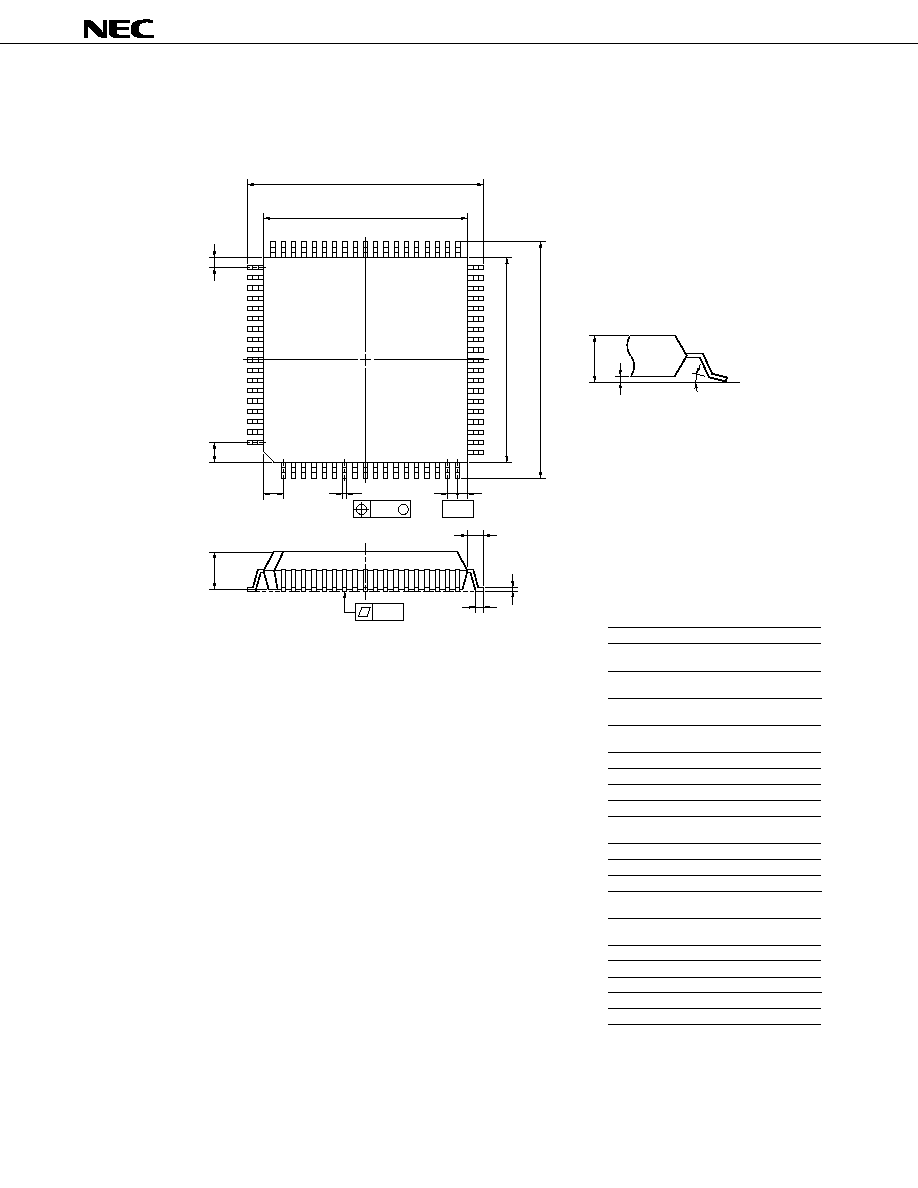
µ
PD78P324, 78P324(A)
65
8.
PACKAGE DRAWINGS
74-Pin Plastic QFP(
s
s
20)
ITEM
MILLIMETERS
INCHES
F
1
F
2
I
2.0
1.0
0.20
Q
0.079
0.039
0.008
S74GJ-100-5BJ-3
NOTE
Each lead centerline is located within 0.20 mm (0.008 inch) of
its true position (T.P.) at maximum material condition.
C
20.0±0.2
0.787
M
0.15
0.006
0.1±0.1
0.004±0.004
+0.004
≠0.003
+0.009
≠0.008
A
23.2±0.4
0.913
H
0.40±0.10
0.016+0.004
≠0.005
L
0.8±0.2
0.031+0.009
≠0.008
N
0.10
0.004
P
3.7
0.146
S
4.0 MAX.
0.158 MAX.
+0.10
≠0.05
B
20.0±0.2
0.787+0.009
≠0.008
+0.017
≠0.016
J
1.0 (T.P.)
0.039 (T.P.)
R
5
∞
±5
∞
5
∞
±5
∞
D
23.2±0.4
0.913+0.017
≠0.016
G
1
G
2
2.0
1.0
0.079
0.039
K
1.6±0.2
0.063±0.008
A
B
G
1
H
I
J
C
D
P
N
K
L
M
detail of lead end
M
56
57
37
74
1
19
18
38
F
2
F
1
G
2
S
Q
R
Remark
The package and material of the ES product
are equivalent to those for mass production.

µ
PD78P324, 78P324(A)
66
P68L-50A1-2
ITEM
MILLIMETERS
INCHES
NOTE
Each lead centerline is located within 0.12
mm (0.005 inch) of its true position (T.P.) at
maximum material condition.
+0.007
≠0.006
A
B
C
D
E
F
G
H
I
J
K
M
N
P
Q
T
U
25.2±0.2
24.20
24.20
25.2±0.2
1.94±0.15
0.6
4.4±0.2
2.8±0.2
0.9 MIN.
3.4
1.27 (T.P.)
0.40±1.0
0.12
23.12±0.20
0.15
R 0.8
0.20
+0.10
≠0.05
0.992±0.008
0.953
0.953
0.992±0.008
0.076
0.024
0.173
0.110
0.035 MIN.
0.134
0.050 (T.P.)
0.016
0.005
0.910
0.006
R 0.031
0.008
+0.009
≠0.008
+0.009
≠0.008
+0.004
≠0.005
+0.004
≠0.002
+0.009
≠0.008
N
K
M
Q
A
U
68
B
D
C
1
F
E
T
P
M
G
H
IJ
68 PIN PLASTIC QFJ ( 950 mil)
Remark
The package and material
of the ES product are
equivalent to those for mass
production.
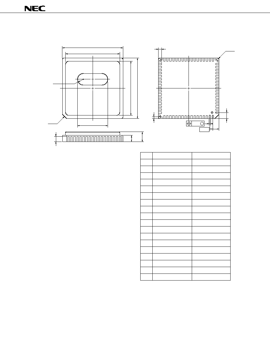
µ
PD78P324, 78P324(A)
67
74 PIN CERAMIC WQFN
X74KW-100A-1
ITEM
MILLIMETERS
INCHES
NOTE
Each lead centerline is located within 0.10
mm (0.004 inch) of its true position (T.P.) at
maximum material condition.
A
B
C
D
E
F
G
H
I
J
K
Q
R
S
T
U
W
Y
20.0±0.4
18.0
18.0
20.0±0.4
1.94
2.14
4.0 MAX.
0.51±0.10
0.10
1.0 (T.P.)
1.0±0.2
C 0.3
2.0
2.0
R 2.0
10.0
0.7±0.2
C 1.5
0.787
0.709
0.709
0.787
0.076
0.084
0.158 MAX.
0.020±0.004
0.004
0.039 (T.P.)
0.039
C 0.012
0.079
0.079
R 0.079
0.394
0.028
C 0.059
+0.017
≠0.016
+0.017
≠0.016
+0.009
≠0.008
+0.008
≠0.009
A
B
D
C
T
Y
U
E
F
G
I
M
K
Q
S
74
H
J
1
W
R
Remark
The package and material of the
ES product are equivalent to
those for mass production.
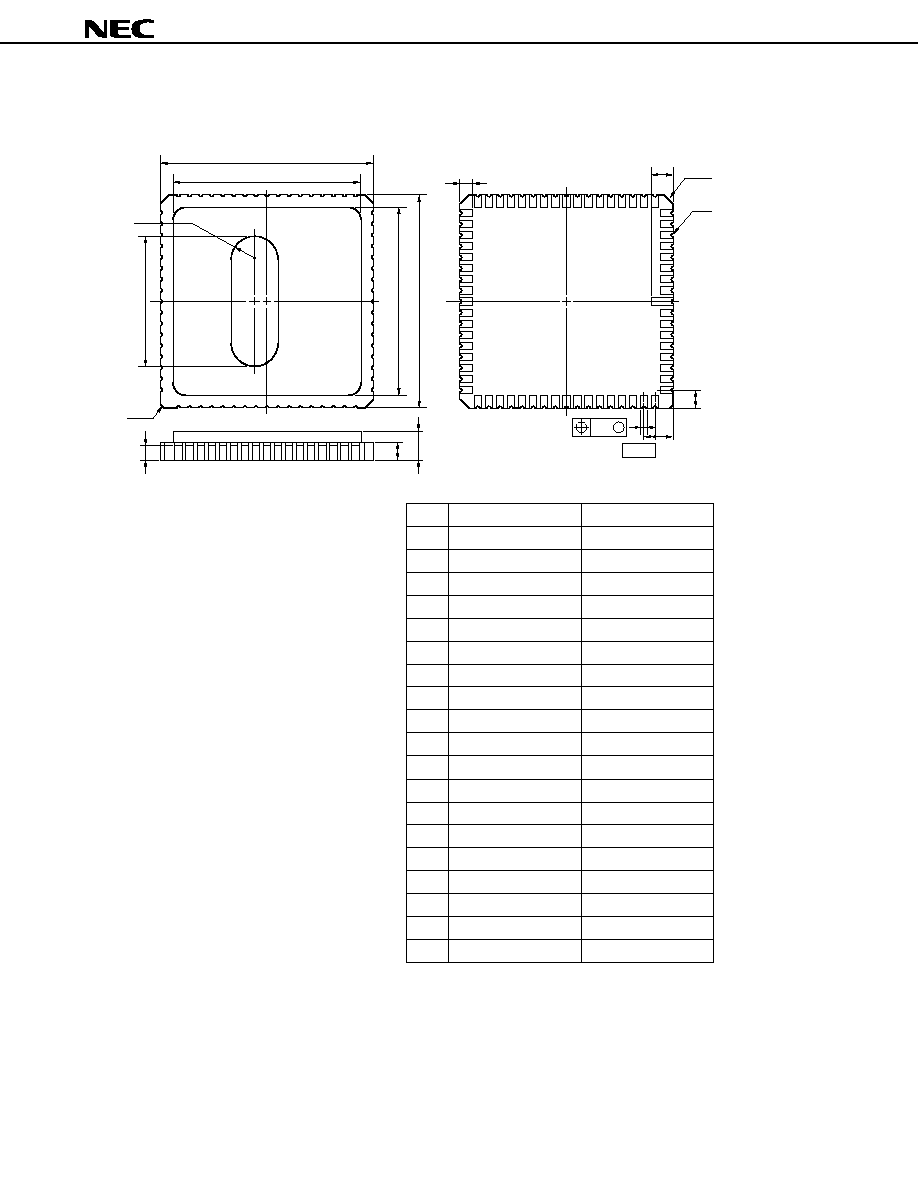
µ
PD78P324, 78P324(A)
68
68 PIN CERAMIC WQFN
X68KW-50A-1
ITEM
MILLIMETERS
INCHES
NOTE
Each lead centerline is located within 0.12
mm (0.005 inch) of its true position (T.P.) at
maximum material condition.
A
B
C
D
E
F
G
H
I
J
K
L
P
Q
R
S
T
U
Y
24.13±0.4
21.5
21.5
24.13±0.4
1.65
2.03
3.50 MAX.
0.64±0.10
0.12
1.27 (T.P.)
1.27±0.2
2.16±0.2
R 0.2
C 1.02
1.905
1.905
R 3.0
12.0
C 0.5
0.950±0.016
0.846
0.846
0.950±0.016
0.065
0.080
0.138 MAX.
0.025
0.005
0.05 (T.P.)
0.05±0.008
0.085±0.008
R 0.008
C 0.04
0.075
0.075
R 0.118
0.472
C 0.020
G
A
U
F
E
Y
T
B
C
D
68
J
I
M
H
R
K
L
Q
P
1
S
+0.005
≠0.004
Remark
The package and material of the
ES product are equivalent to those
for mass production.
µ
PD78P324, 78P324(A)
69
9.
RECOMMENDED SOLDERING CONDITIONS
Please solder the package of this product under the conditions recommended as follows.
For details of the recommended conditions for soldering, please refer to the information document
"Semiconductor Device Mounting Technology Manual" (IEI-1207).
For soldering methods and conditions other than those recommended below, please contact NEC sales
personnel.
Table 9-1. Soldering Conditions for Surface-Mount Type (1)
µ
PD78P324GJ-5BJ
: 74-pin plastic QFP (20 x 20 mm)
µ
PD78P324LP
: 68-pin plastic QFJ (
s
s
950 mil)
µ
PD78P324LP(A)
: 68-pin plastic QFJ (
s
s
950 mil)
µ
PD78P324LP(A1)
: 68-pin plastic QFJ (
s
s
950 mil)
µ
PD78P324LP(A2)
: 68-pin plastic QFJ (
s
s
950 mil)
Soldering Method
Soldering Condition
Infrared reflow
Package peak temperature : 230
∞
C; time : within 30 secs (210
∞
C or more);
count: once; day limit : 7 days
Note
(hereafter, pre-baked for 36 hrs at 125
∞
C)
VPS
Package peak temperature : 215
∞
C; time : within 40 secs (200
∞
C or more);
count: once; day limit : 7 days
Note
(hereafter, pre-baked for 36 hrs at 125
∞
C)
Wave soldering
Solder bath temperature: no more than 260
∞
C; time : within 10 secs; count:
once; preheating temperature : 120
∞
C max. (package surface temperature);
day limit : 7 days
Note
(hereafter, pre-baked for 36 hours at 125
∞
C)
Pin part heating
Pin temperature : no more than 300
∞
C; time : within 3 secs (per device side)
Recommended
Condition Symbol
IR30-367-1
VP15-367-1
WS60-367-1
--
Note
Refers to the number of days for storage after the dry pack is opened. The storage conditions are 25
∞
C
and no more than 65 %RH.
Caution
Avoid using multiple soldering methods at the same time (except the pin part heating method).

µ
PD78P324, 78P324(A)
70
Table 9-2. Soldering Conditions for Surface-Mount Type (2)
µ
PD78P324GJ(A)-5BJ
: 74-pin plastic QFP (20 x 20 mm)
µ
PD78P324GJ(A1)-5BJ
: 74-pin plastic QFP (20 x 20 mm)
µ
PD78P324GJ(A2)-5BJ
: 74-pin plastic QFP (20 x 20 mm)
Soldering Method
Soldering Condition
Infrared reflow
Package peak temperature: 235
∞
C; time: within 30 secs (210
∞
C or more);
count: twice; day limit: 7 days
Note
(hereafter, pre-baked for 36 hrs at 125
∞
C)
<Caution>
(1) The second reflow should be started after the temperature of the device
which would have been changed by the first reflow has returned to
normal.
(2) Please avoid flux water washing after the first reflow.
VPS
Package peak temperature: 215
∞
C; time: within 40 secs (200
∞
C or more);
count: within twice; day limit: 7 days
Note
(hereafter, pre-baked for 36 hrs at
125
∞
C)
<Caution>
(1) The second reflow should be started after the temperature of the device
which would have been changed by the first reflow has returned to
normal.
(2) Please avoid flux water washing after the first reflow.
Wave soldering
Solder bath temperature: no more than 260
∞
C; time: within 10 secs; count:
once; preheating temperature: up to 120
∞
C (package surface temperature);
day limit: 7 days
Note
(hereafter, pre-baked for 36 hours at 125
∞
C)
Pin part heating
Pin temperature: no more than 300
∞
C; time: within 3 secs (per device side)
Recommended
Condition Symbol
IR35-367-2
VP15-367-2
WS60-367-1
--
Note
Refers to the number of days for storage after the dry pack is opened. The storage conditions are 25
∞
C
and no more than 65 %RH.
Caution
Avoid using two or more soldering methods at the same time (except the pin part heating method).
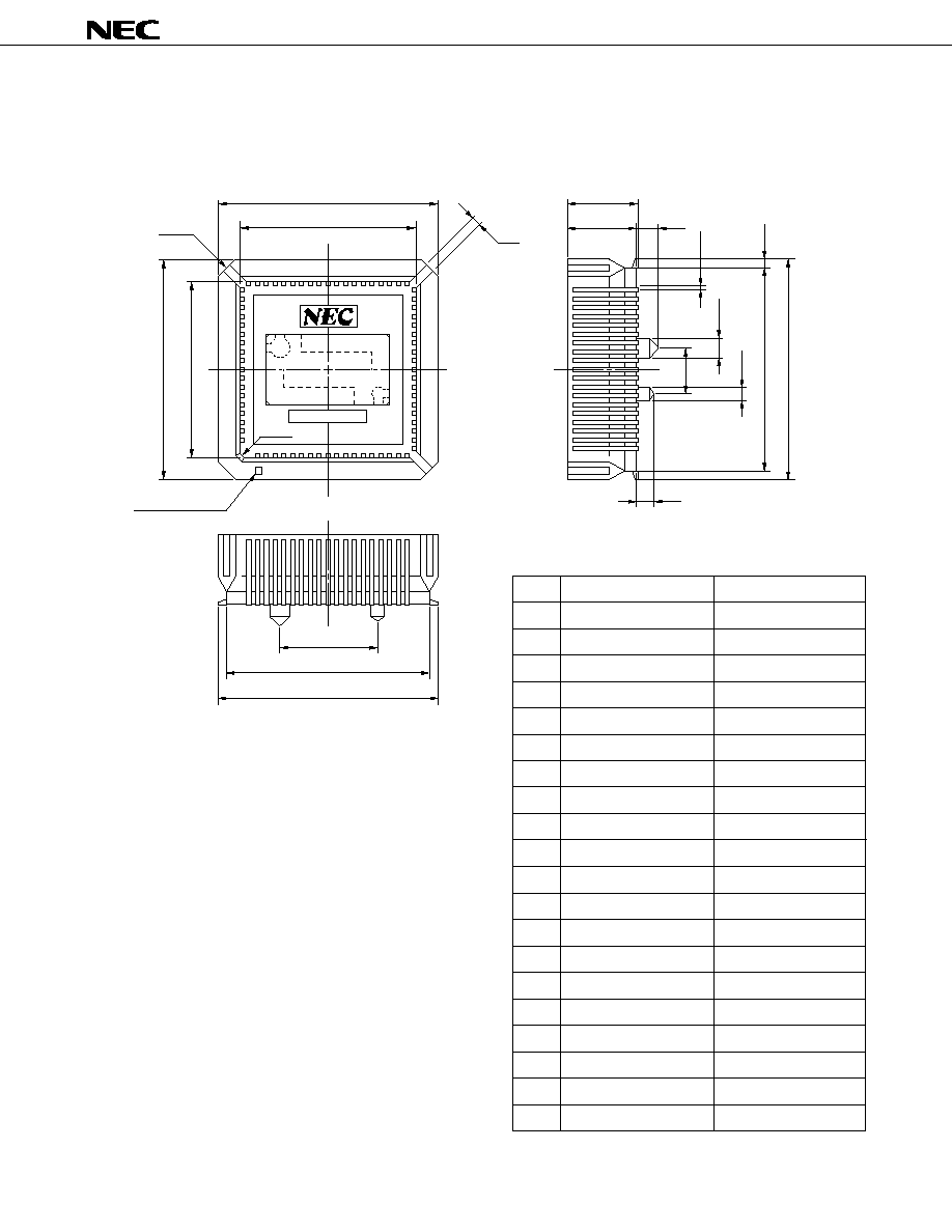
µ
PD78P324, 78P324(A)
71
APPENDIX A. CONVERSION SOCKET PACKAGE DRAWING AND RECOMMENDED SUBSTRATE
INSTALLATION PATTERN
Figure A-1. Conversion Socket (EV-9200G-74) Package Drawing (Reference)
A
F
D
1
E
B
C
C 1.5
M
N
L
K
R
Q
P
S
T
O
I
H
EV-9200G-74
J
G
No.1 pin index
EV-9200G-74-G0
ITEM
MILLIMETERS
INCHES
A
B
C
D
E
F
G
H
I
J
K
L
M
N
O
P
Q
R
S
T
25.0
20.35
20.35
25.0
4-C 2.8
1.0
11.0
22.0
24.7
5.0
22.0
24.7
8.0
7.8
2.5
2.0
1.35
0.35±0.1
2.3
1.5
0.984
0.801
0.801
0.984
4-C 0.11
0.039
0.433
0.866
0.972
0.197
0.866
0.972
0.315
0.307
0.098
0.079
0.053
0.014
0.091
0.059
+0.004
≠0.005

µ
PD78P324, 78P324(A)
72
Figure A-2. Recommended Pattern for Conversion Socket (EV-9200G-74)
Substrate Installation (Reference)
F
E
G
J
K
H
I
D
A
B
C
0.039
◊
0.709=0.709
0.039
◊
0.709=0.709
EV-9200G-74-P0
ITEM
MILLIMETERS
INCHES
A
B
C
D
E
F
G
H
I
J
K
25.7
21.0
21.0
25.7
11.00±0.08
5.00±0.08
0.6±0.02
2.36±0.03
1.57±0.03
1.012
0.827
0.827
1.012
0.433
0.197
0.024
0.093
0.062
1.0±0.02
◊
18=18.0±0.05
1.0±0.02
◊
18=18.0±0.05
+0.002
≠0.001
+0.002
≠0.003
+0.002
≠0.001
+0.002
≠0.003
+0.004
≠0.003
+0.003
≠0.004
+0.001
≠0.002
+0.001
≠0.002
+0.001
≠0.002
Dimensions of mount pad for EV-9200 and that for target
device (QFP) may be different in some parts. For the
recommended mount pad dimensions for QFP, refer to
"SEMICONDUCTOR DEVICE MOUNTING TECHNOLOGY
MANUAL" (IEI-1207).
Caution

µ
PD78P324, 78P324(A)
73
APPENDIX B. TOOLS
B.1
DEVELOPMENT TOOLS
The following development tools have been made available for development of the system using the
µ
PD78P324.
Language Processors
78K/III series relocatable assem-
bler (RA78K/III)
78K/III series C compiler (CC78K/III)
Refers to the relocatable assembler which can be used commonly for the 78K/III
series. Equipped with the macro function, the relocatable assembler is aimed at
improved development efficiency. The assembler is also accompanied by the
structured assembler which can describe the program control structure explicitly,
thus making it possible to improve the productivity and the maintainability of the
program.
Host machine
PC-9800 series
IBM PC/AT
TM
and
its compatible
machine
HP9000 series
300
TM
SPARCstation
TM
Supply medium
3.5-inch 2HD
5-inch 2HD
3.5-inch 2HC
5-inch 2HC
Cartridge tape
(QIC-24)
Part number
µ
S5A13RA78K3
µ
S5A10RA78K3
µ
S7B13RA78K3
µ
S7B10RA78K3
µ
S3H15RA78K3
µ
S3K15RA78K3
OS
MS-DOS
TM
PC DOS
TM
HP-UX
TM
SunOS
TM
Host machine
PC-9800 series
IBM PC/AT and its
compatible
machine
HP9000 series 300
SPARCstation
Supply medium
3.5-inch 2HD
5-inch 2HD
3.5-inch 2HC
5-inch 2HC
Cartridge tape
(QIC-24)
Part number
µ
S5A13CC78K3
µ
S5A10CC78K3
µ
S7B13CC78K3
µ
S7B10CC78K3
µ
S3H15CC78K3
µ
S3K15CC78K3
OS
MS-DOS
PC DOS
HP-UX
SunOS
Refers to the C compiler which can be commonly used in the 78K/III series. This
compiler is a program converting the programs written in the C language to those
object codes which are executable by microcomputers. When using this compiler,
the 78K/III series relocatable assembler (RA78K/III) is required.
Remark
Relocatable assembler and C compiler operations are assured only on the host machine and the OS
above.

µ
PD78P324, 78P324(A)
74
PG-1500
UNISITE
2900
3900
Note
PA-78P324GJ
PA-78P324LP
PA-78P324KC
PA-78P324KD
PG-1500 controller
PROM Write Tools
This PROM programmer is capable of programming by manipulating a PROM-
incorporated single-chip microcomputer from a stand-alone or host machine after
connecting the accompanying board and the separately available programmer
adapter.
It can also program representative PROMs ranging from 256 Kbits to 4 Mbits.
These are PROM programmers made by Data I/O Japan.
These are the PROM programmer adapters for writing programs into the
µ
PD78P324 on general-purpose PROM programmer such as PG-1500.
PA-78P324GJ: for
µ
PD78P324GJ
PA-78P324LP: for
µ
PD78P324LP
PA-78P324KC: for
µ
PD78P324KC
PA-78P324KD: for
µ
PD78P324KD
A PG-1500 and a host machine are connected with the serial interface or the parallel
interface to control the PG-1500 on the host machine.
Host machine
PC-9800 series
IBM PC/AT and its
compatible
machine
Supply medium
3.5-inch 2HD
5-inch 2HD
3.5-inch 2HC
5-inch 2HC
Part number
µ
S5A13PG1500
µ
S5A10PG1500
µ
S7B13PG1500
µ
S7B10PG1500
OS
MS-DOS
PC DOS
Hardware
Software
Note
Being evaluated.
Remark
The PG-1500 controller operation is assured only on the host machine and the OS above.
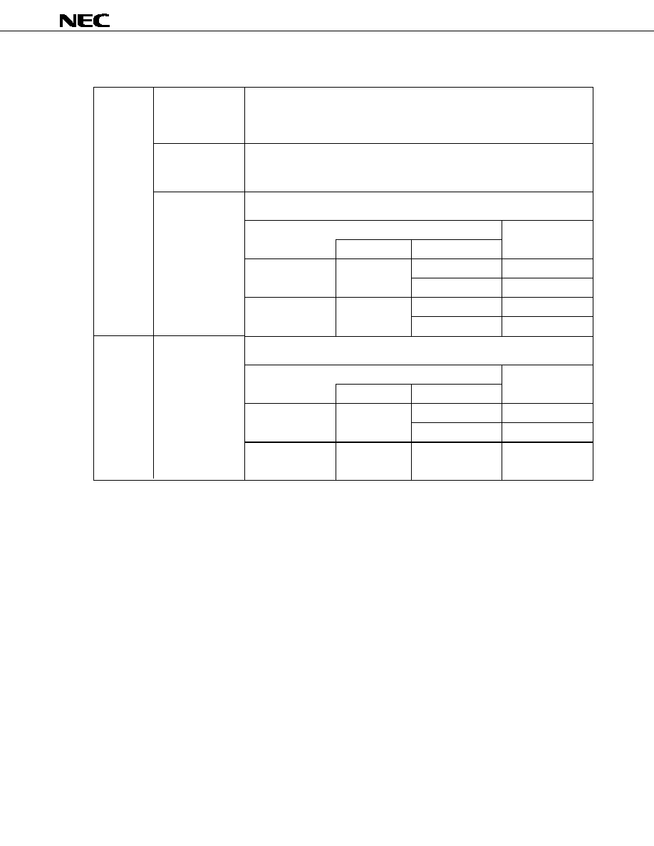
µ
PD78P324, 78P324(A)
75
Debugging Tools
IE-78327-R
IE-78320-R
Note
EP-78320GJ-R
EP-78320L-R
IE-78327-R
control program
(IE controller)
IE-78320-R
control program
Note
(IE controller)
These are the in-circuit emulators which can be used for the development and
debugging of application systems. Debugging is performed by connecting them to a
host machine. The IE-78327-R can be used commonly for both the
µ
PD78322
subseries and the
µ
PD78328 subseries.
The IE-78320-R can be used for the
µ
PD78322 subseries.
These are the emulation probes for connecting the IE-78327-R or IE-78320-R to a
target system.
EP-78320GJ-R: for 74-pin plastic QFP
EP-78320L-R: for 68-pin plastic QFJ
This program is for controlling the IE-78327-R from a host machine. It can execute
commands automatically, thus enabling more efficient debugging.
Hardware
Software
Host machine
PC-9800 series
IBM PC/AT and its
compatible
machine
Supply medium
3.5-inch 2HD
5-inch 2HD
3.5-inch 2HC
5-inch 2HC
Part number
µ
S5A13IE78327
µ
S5A10IE78327
µ
S7B13IE78327
µ
S7B10IE78327
OS
MS-DOS
PC DOS
This program is for controlling the IE-78320-R from a host machine. It can execute
commands automatically, thus enabling more efficient debugging.
Host machine
PC-9800 series
IBM PC/AT and its
compatible
machine
Supply medium
3.5-inch 2HD
5-inch 2HD
5-inch 2HC
Part number
µ
S5A13IE78320
µ
S5A10IE78320
µ
S7B10IE78320
OS
MS-DOS
PC DOS
Remarks
1. The operation of each software is assured only on the host machine and the OS above.
2.
µ
PD78322 subseries:
µ
PD78320, 78322, 78P322, 78323, 78324, 78P324, 78320(A), 78320(A1),
78320(A2), 78322(A), 78322(A1), 78322(A2), 78323(A), 78323(A1), 78323(A2),
78324(A), 78324(A1), 78324(A2), 78P324(A), 78P324(A1), 78P324(A2)
µ
PD78328 subseries:
µ
PD78327, 78328, 78P328, 78327(A), 78328(A)
Note
The existing product IE-78320-R is a maintenance product. If you are going to newly purchase an in-circuit
emulator, please use the alternative product IE-78327-R.
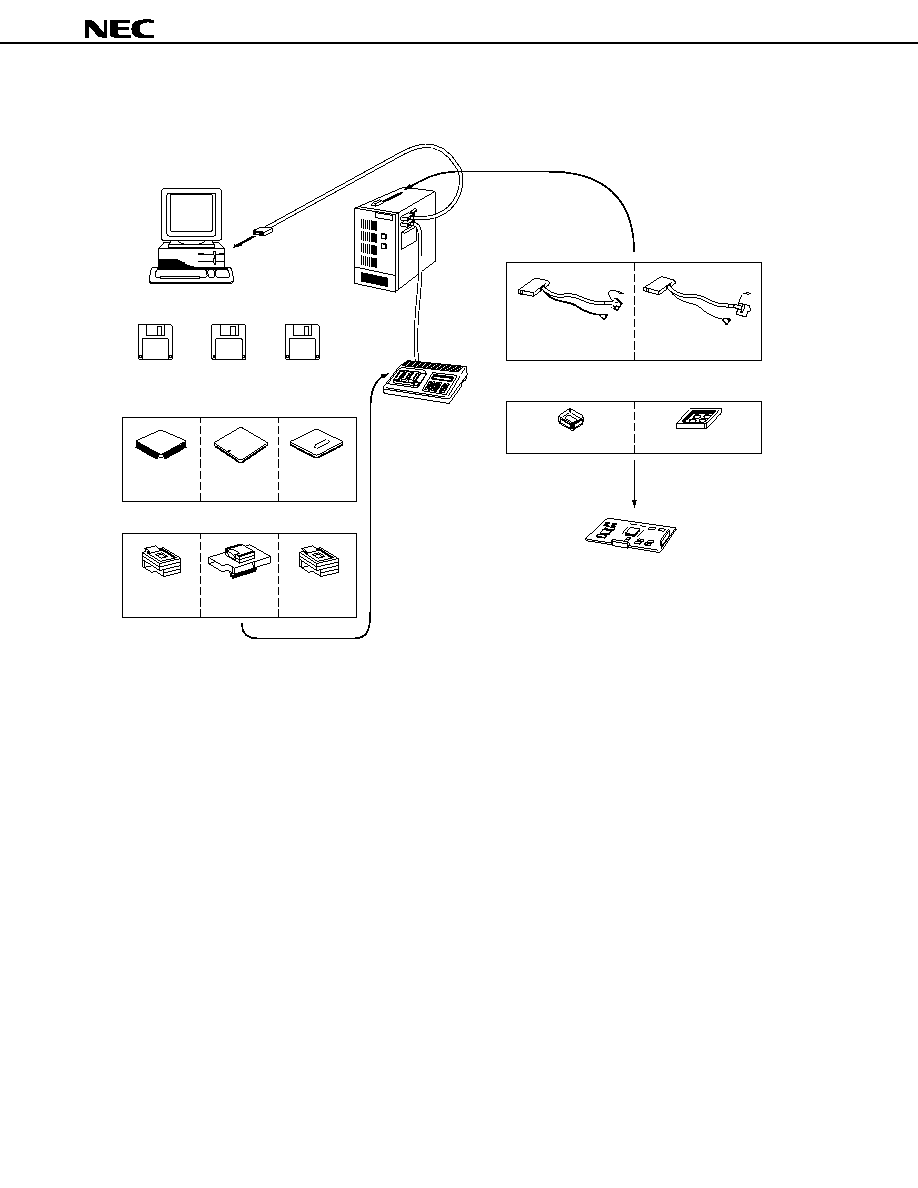
µ
PD78P324, 78P324(A)
76
Development Tool Configurations
Note
The socket is supplied with the emulation probe.
Remarks
1. It is also possible to use the host machine and the PG-1500 by connecting them directly by the RS-
232-C.
2. In the diagram above, representative software supply media and 3.5-inch FDs.
Host machine
PC-9800 series
IBM PC/AT or its compatible machine
Software
Relocatable assembler
(With structured assembler)
PG-1500
controller
IE controller
PD78P324GJ
PD78P324LP
PD78P324KD
PD78P324KC
PA-78P324GJ
PA-78P324LP
PA-78P324KC
PA-78P324KD
+
+
+
Programmer adapters
PROM-incorporated products
RS-232-C
IE-78327-R
in-circuit emulator
RS-232-C
PG-1500
PROM programmer
Emulation probes
Socket for connecting the emulation probe
and the target system
EP-78320GJ-R
EP-78320L-R
EV-9200G-74
Socket for plastic QFJ
Target system
µ
µ
µ
µ
Note

µ
PD78P324, 78P324(A)
77
B.2
EVALUATION TOOLS
To evaluate the functions of the
µ
PD78P324, the following tools are made available.
Part Number
EB-78320-98
EB-78320-PC
Function
By connecting to a host machine, it is possible
to evaluate the functions equipped by the
µ
PD78P324 in a simple manner. The com-
mand system of this product basically
conforms to that of IE-78327-R and IE-78320-
R. Therefore, it is easy to move to the
development work of application systems by
IE-78327-R or IE-78320-R. In addition a turbo
access manager (
µ
PD71P301)
Note
can be
mounted on the board.
Note
The turbo access manager (
µ
PD71P301) is a maintenance product.
Cautions
1. This product is not a development tool of
µ
PD78P324 application systems.
2. This product is not equipped with the emulation function for executing the PROM incorporated
in the
µ
PD78P324.
B.3
EMBEDDED SOFTWARE
The following embedded software programs are available to perform program development and
maintenance more efficiently.
Eeal-time OS
Host Machine
PC-9800 series
IBM PC/AT or its compatible
machine
Real-time OS (RX78K/III)
The RX78K/III is designed to provide a multi-task environment in the field of control
application where real-time operation is required. By using this real-time OS, the
performance of the whole system can be improved by allocating CPU's idle time to
other processings.
The RX78K/III provides the system call based on the
µ
ITRON specifications.
The RX78K/III package provides tools (configurators) for creating RX78K/III's nucleus
and multiple information table.
Host machine
PC-9800 series
IBM PC/AT and its
compatible
machine
Supply medium
3.5-inch 2HD
5-inch 2HD
3.5-inch 2HC
5-inch 2HC
Part number
µ
S5A13RX78320
µ
S5A10RX78320
µ
S7B13RX78320
µ
S7B10RX78320
OS
MS-DOS
PC DOS
Caution
To purchase the operating system above, you need to fill in a purchase application form beforehand
and sign a contract allowing you to use the software.
Remark
When using the real-time OS RX78K/III, you need the assembler package RA78K/III (optional) as well.

µ
PD78P324, 78P324(A)
78
Fuzzy knowledge data creation
tools (FE9000, FE9200)
Translator (FT78K3)
Note
Fuzzy inference module
(FI78K/III)
Note
Fuzzy inference debugger
(FD78K/III)
This program supports inputting/editing/evaluating (through simulation) of the fuzzy
knowledge data (fuzzy rules and membership functions).
Fuzzy Inference Development Support System
Host machine
PC-9800 series
IBM PC/AT and its
compatible
machine
Supply medium
3.5-inch 2HD
5-inch 2HD
3.5-inch 2HC
5-inch 2HC
Part number
µ
S5A13FE9000
µ
S5A10FE9000
µ
S7B13FE9000
µ
S7B10FE9000
OS
MS-DOS
PC DOS Winsows
This program converts the fuzzy knowledge data obtained with fuzzy knowledge
data creation tools to an assembler source program for RA78K/III.
Host machine
PC-9800 series
IBM PC/AT and its
compatible
machine
Supply medium
3.5-inch 2HD
5-inch 2HD
3.5-inch 2HC
5-inch 2HC
Part number
µ
S5A13FT78K3
µ
S5A10FT78K3
µ
S7B13FT78K3
µ
S7B10FT78K3
OS
MS-DOS
PC DOS
Supply medium
3.5-inch 2HD
5-inch 2HD
3.5-inch 2HC
5-inch 2HC
Part number
µ
S5A13FI78K3
µ
S5A10FI78K3
µ
S7B13FI78K3
µ
S7B10FI78K3
OS
MS-DOS
PC DOS
Supply medium
3.5-inch 2HD
5-inch 2HD
3.5-inch 2HC
5-inch 2HC
Part number
µ
S5A13FD78K3
µ
S5A10FD78K3
µ
S7B13FD78K3
µ
S7B10FD78K3
OS
MS-DOS
PC DOS
Note
Under development
Host machine
PC-9800 series
IBM PC/AT and its
compatible
machine
This program executes fuzzy inference. Fuzzy inference is executed by being linked
to the fuzzy knowledge data converted by the translator.
This is a support software program for evaluating and adjusting the fuzzy knowl-
edge data at a hardware level by using the in-circuit emulator.
Host machine
PC-9800 series
IBM PC/AT and its
compatible
machine
µ
PD78P324, 78P324(A)
79
NOTES FOR CMOS DEVICES
1
PRECAUTION AGAINST ESD FOR SEMICONDUCTORS
Note: Strong electric field, when exposed to a MOS device, can cause destruction of
the gate oxide and ultimately degrade the device operation. Steps must be
taken to stop generation of static electricity as much as possible, and quickly
dissipate it once, when it has occurred. Environmental control must be
adequate. When it is dry, humidifier should be used. It is recommended to
avoid using insulators that easily build static electricity. Semiconductor
devices must be stored and transported in an anti-static container, static
shielding bag or conductive material. All test and measurement tools including
work bench and floor should be grounded. The operator should be grounded
using wrist strap. Semiconductor devices must not be touched with bare
hands. Similar precautions need to be taken for PW boards with semiconductor
devices on it.
2
HANDLING OF UNUSED INPUT PINS FOR CMOS
Note: No connection for CMOS device inputs can be cause of malfunction. If no
connection is provided to the input pins, it is possible that an internal input
level may be generated due to noise, etc., hence causing malfunction. CMOS
device behave differently than Bipolar or NMOS devices. Input levels of CMOS
devices must be fixed high or low by using a pull-up or pull-down circuitry. Each
unused pin should be connected to V
DD
or GND with a resistor, if it is considered
to have a possibility of being an output pin. All handling related to the unused
pins must be judged device by device and related specifications governing the
devices.
3
STATUS BEFORE INITIALIZATION OF MOS DEVICES
Note: Power-on does not necessarily define initial status of MOS device. Production
process of MOS does not define the initial operation status of the device.
Immediately after the power source is turned ON, the devices with reset
function have not yet been initialized. Hence, power-on does not guarantee
out-pin levels, I/O settings or contents of registers. Device is not initialized
until the reset signal is received. Reset operation must be executed immedi-
ately after power-on for devices having reset function.
QTOP is a trademark of NEC Corporation.
MS-DOS and Windows are trademarks of Microsoft Corp.
PC/AT and PC DOS are trademarks of IBM Corp.
HP9000 series 300 and HP-UX are trademarks of Hewlett-Packard.
SPARCstation is a trademark of SPARC International, Inc.
SunOS is a trademark of Sun Microsystems Inc.
TRON is an abbreviation of The Realtime Operating system Nucleus.
ITRON is an abbreviation of Industrial TRON.

The export of these products from Japan is regulated by the Japanese government. The export of some or all of these
products may be prohibited without governmental license. To export or re-export some or all of these products from
a country other than Japan may also be prohibited without a license from that country. Please call an NEC sales
representative.
License not needed:
µ
PD78P324KC, 78P324KD
The customer must judge the need for license:
µ
PD78P324GJ-5BJ/(A)/(A1)/(A2)/,
78P324LP/(A)/(A1)/(A2)
No part of this document may be copied or reproduced in any form or by any means without the prior written
consent of NEC Corporation. NEC Corporation assumes no responsibility for any errors which may appear in this
document.
NEC Corporation does not assume any liability for infringement of patents, copyrights or other intellectual
property rights of third parties by or arising from use of a device described herein or any other liability arising
from use of such device. No license, either express, implied or otherwise, is granted under any patents,
copyrights or other intellectual property rights of NEC Corporation or others.
While NEC Corporation has been making continuous effort to enhance the reliability of its semiconductor devices,
the possibility of defects cannot be eliminated entirely. To minimize risks of damage or injury to persons or
property arising from a defect in an NEC semiconductor device, customer must incorporate sufficient safety
measures in its design, such as redundancy, fire-containment, and anti-failure features.
NEC devices are classified into the following three quality grades:
"Standard", "Special", and "Specific". The Specific quality grade applies only to devices developed based on
a customer designated "quality assurance program" for a specific application. The recommended applications
of a device depend on its quality grade, as indicated below. Customers must check the quality grade of each
device before using it in a particular application.
Standard: Computers, office equipment, communications equipment, test and measurement equipment,
audio and visual equipment, home electronic appliances, machine tools, personal electronic
equipment and industrial robots
Special:
Transportation equipment (automobiles, trains, ships, etc.), traffic control systems, anti-disaster
systems, anti-crime systems, safety equipment and medical equipment (not specifically designed
for life support)
Specific: Aircrafts, aerospace equipment, submersible repeaters, nuclear reactor control systems, life
support systems or medical equipment for life support, etc.
The quality grade of NEC devices in "Standard" unless otherwise specified in NEC's Data Sheets or Data Books.
If customers intend to use NEC devices for applications other than those specified for Standard quality grade,
they should contact NEC Sales Representative in advance.
Anti-radioactive design is not implemented in this product.
M4 94.11
µ
PD78P324, 78P324(A)