Document Outline
- COVER
- FEATURES
- ORDERING INFORMATION
- QUALITY GRADE
- 78K/IV SERIES PRODUCT DEVELOPMENT DIAGRAM
- FUNCTIONS
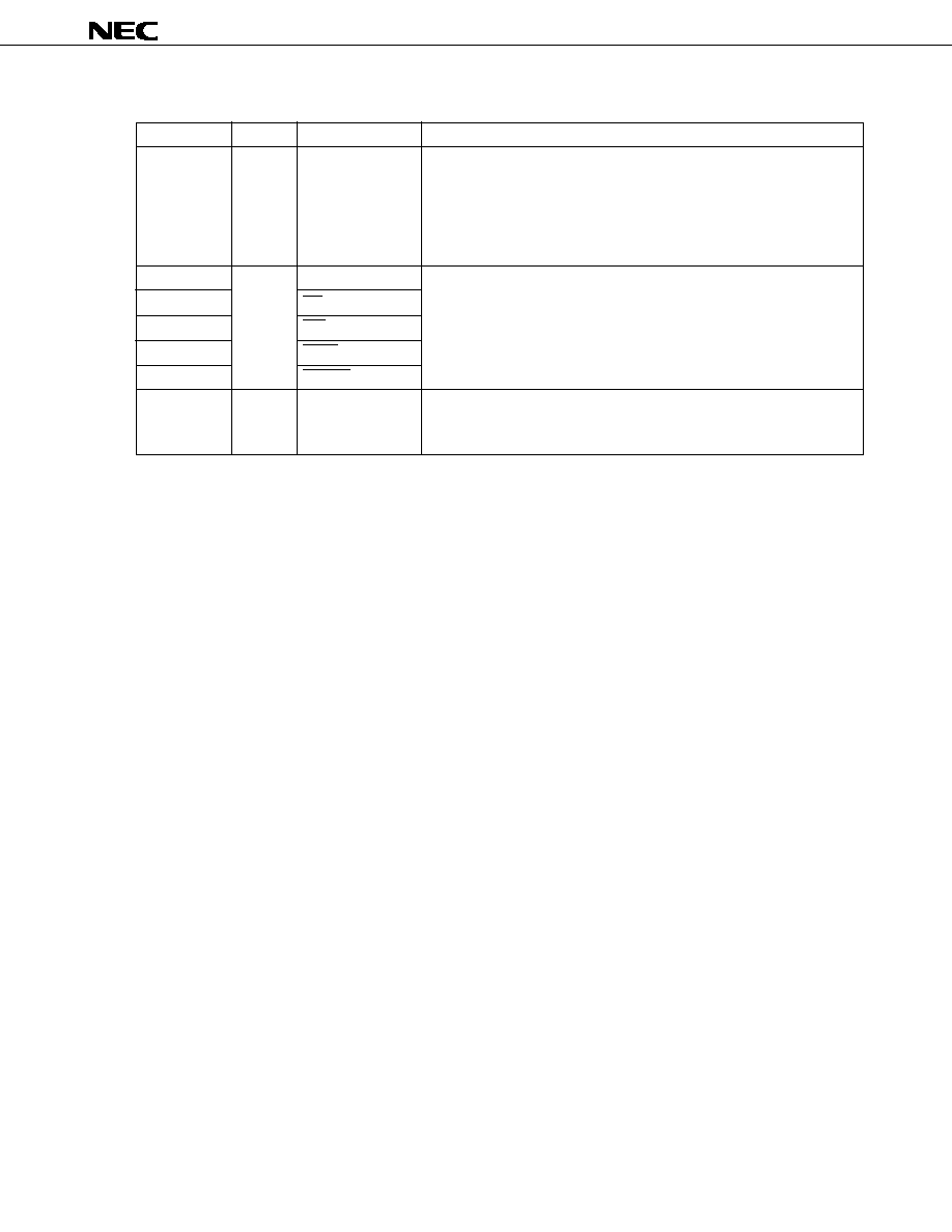
- 1. DIFFERENCES BETWEEN uPD78P4038Y AND MASKED ROM PRODUCTS
- 2. PIN CONFIGURATION (TOP VIEW)
- 3. BLOCK DIAGRAM
- 4. LIST OF PIN FUNCTIONS
- 4.1 Pins for Normal Operating Mode
- 4.2 Pins for PROM Programming Mode (Vpp Greater or equal to +5V or +12.5V, RESET# = L)
- 4.2.1 Pin functions
- 4.2.2 Pin functions
- 4.3 I/O Circuits for Pins and Handling of Unused Pins
- 5. INTERNAL MEMORY SWITCHING (IMS) REGISTER
- 6. PROM PROGRAMMING
- 6.1 Operation Mode
- 6.2 PROM Write Sequence
- 6.3 PROM Read Sequence
- 7. ERASURE CHARACTERISTICS (uPD78P4038YKK-T ONLY)
- 8. PROTECTIVE FILM COVERING THE ERASURE WINDOW (uPD78P4038YKK-T ONLY)
- 9. QUALITY
- 10. SCREENING ONE-TIME PROM PRODUCTS
- 11. ELECTRICAL CHARACTERISTICS
- 12. PACKAGE DRAWINGS
- 13. RECOMMENDED SOLDERING CONDITIONS
- APPENDIX A DEVELOPMENT TOOLS
- APPENDIX B CONVERSION SOCKET (EV-9200GC-80) AND CONVERSION ADAPTER (TGK-080SDW)
- APPENDIX C RELATED DOCUMENTS
DATA SHEET
MOS INTEGRATED CIRCUIT
µ
PD78P4038Y
The
µ
PD78P4038Y, 78K/IV Series' product, is a one-time PROM or EPROM version of the
µ
PD784035Y,
µ
PD784036Y,
µ
PD784037Y, and
µ
PD784038Y with internal masked ROM.
Since user programs can be written to PROM, this microcontroller is best suited for evaluation in system
development, manufacture of small quantities of multiple products, and fast start-up of applications.
For specific functions and other detailed information, consult the following user's manual.
This manual is required reading for design work.
µ
PD784038, 784038Y Sub-Series User's Manual, Hardware : U11316E
78K/IV Series User's Manual, Instruction
: U10905E
FEATURES
∑
Compatible with the
µ
PD78P238,
µ
PD78P4026, and
µ
PD78P4038
∑
Internal PROM: 128 Kbytes
∑
µ
PD78P4038YKK-T
: EPROM (best suited for system evaluation)
∑
µ
PD78P4038YGC-3B9 : PROM (best suited for manufacture of small quantities)
µ
PD78P4038YGC-8BT : PROM (best suited for manufacture of small quantities)
µ
PD78P4038YGK-BE9 : PROM (best suited for manufacture of small quantities)
∑
Internal RAM:
4,352 bytes
∑
Supply voltage: V
DD
= 2.7 to 5.5 V
∑
QTOP
TM
microcomputer
Remark The QTOP microcomputer is a microcomputer with a built-in one-time PROM that is totally supported
by NEC. The support includes writing application programs, marking, screening, and verification.
ORDERING INFORMATION
Part number
Package
Internal ROM
µ
PD78P4038YGC-3B9
80-pin plastic QFP (14
◊
14
◊
2.7 mm)
One-time PROM
µ
PD78P4038YGC-8BT
80-pin plastic QFP (14
◊
14
◊
1.4 mm)
One-time PROM
µ
PD78P4038YGC-
◊◊◊
-3B9
80-pin plastic QFP (14
◊
14 mm)
One-time PROM (QTOP microcomputer)
µ
PD78P4038YGK-BE9
80-pin plastic TQFP (fine pitch) (12
◊
12 mm)
One-time PROM
µ
PD78P4038YGK-
◊◊◊
-BE9
80-pin plastic TQFP (fine pitch) (12
◊
12 mm)
One-time PROM (QTOP microcomputer)
µ
PD78P4038YKK-T
80-pin ceramic WQFN (14
◊
14 mm)
EPROM
In this reference, all ROM components that are common to one-time PROM and EPROM are referred to as
PROM.
The mark shows major revised points.
The information in this document is subject to change without notice.
16/8-BIT SINGLE-CHIP MICROCONTROLLER
Document No.
U10742EJ2V0DS00 (2nd edition)
Date Published July 1998 J CP(K)
Printed in Japan
©
1995

µ
PD78P4038Y
2
QUALITY GRADE
Part number
Package
Quality grade
µ
PD78P4038YGC-3B9
80-pin plastic QFP (14
◊
14
◊
2.7 mm)
Standard (for general electronic equipment)
µ
PD78P4038YGC-8BT
80-pin plastic QFP (14
◊
14
◊
1.4 mm)
Standard (for general electronic equipment)
µ
PD78P4038YGC-
◊◊◊
-3B9
80-pin plastic QFP (14
◊
14
◊
1.4 mm)
Standard (for general electronic equipment)
µ
PD78P4038YGK-BE9
80-pin plastic TQFP (fine pitch) (12
◊
12 mm)
Standard (for general electronic equipment)
µ
PD78P4038YGK-
◊◊◊
-BE9 80-pin plastic TQFP (fine pitch) (12
◊
12 mm)
Standard (for general electronic equipment)
µ
PD78P4038YKK-T
80-pin ceramic WQFN (14
◊
14 mm)
Not applied (for function evaluation)
Please refer to "Quality Grades on NEC Semiconductor Devices" (Document No. C11531E) published by NEC Corporation
to know the specification of quality grade on the devices and its recommended applications.
Caution The EPROM versions of the
µ
PD78P4038Y are not intended for use in mass-produced products;
they do not have reliability high enough for such purposes. Their use should be restricted to
functional evaluation in experiment or trial manufacture.
Remark
◊◊◊
is ROM code suffix.
µ
PD78P4038Y
3
78K/IV SERIES PRODUCT DEVELOPMENT DIAGRAM
: Product under mass production
: Product under preparation
Standard Products Development
ASSP Development
PD784026
A/D converters,
16-bit timers, and
power management
functions have been
enhanced.
Internal memory has been expanded.
Pin-compatible with the PD784026
PD784038Y
PD784038
Connectable to the I
2
C bus
100 pins
I/O has been enhanced.
Internal memory has been expanded.
PD784216Y
PD784216
Connectable to the multimaster I
2
C bus
PD784054
Built-in 10-bit A/D converter
PD784046
80 pins
ROM correction function has been added.
PD784225Y
PD784225
Connectable to the multimaster I
2
C bus
Internal memory has been expanded.
ROM correction function has been added.
PD784218Y
PD784218
Connectable to the multimaster I
2
C bus
µ
µ
µ
µ
µ
µ
µ
µ
µ
µ
µ
µ
PD784908
Built-in IEBus
TM
controller
Functions of the PD784915 have been enhanced.
PD784928Y
PD784928
Connectable to the multimaster I
2
C bus
PD784955
DC inverter control
PD784915
Software servo control
Built-in analog circuit for VCR
Timers have been enhanced.
µ
Functions of the PD784908 have been enhanced.
Internal memory has been expanded.
ROM correction function has been added.
PD784937
µ
µ
µ
µ
µ
µ
µ
µ
PD78P4038Y
4
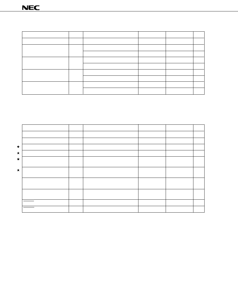
FUNCTIONS
(1/2)
Note
Additional function pins are included in the I/O pins.
Item
Number of basic instructions
(mnemonics)
General-purpose register
Minimum instruction
execution time
Internal
memory
Memory space
I/O ports
Additional
function
pins
Note
Real-time output ports
Timer/counter
PWM outputs
Serial interface
A/D converter
D/A converter
Functions
113
8 bits
◊
16 registers
◊
8 banks, or 16 bits
◊
8 registers
◊
8 banks (memory mapping)
125 ns/250 ns/500 ns/1,000 ns (at 32 MHz)
128 Kbytes (Can be changed to 48 K, 64 K, or 96 Kbytes by software)
4,352 bytes (Can be changed to 2,048 or 3,584 bytes by software)
Program and data: 1 Mbyte
64
8
56
54
24
8
4 bits
◊
2, or 8 bits
◊
1
Timer/counter 0: Timer register
◊
1
Pulse output capability
Capture register
◊
1
∑
Toggle output
Compare register
◊
2
∑
PWM/PPG output
∑
One-shot pulse output
Timer/counter 1: Timer register
◊
1
Pulse output capability
Capture register
◊
1
∑
Real-time output (4 bits
◊
2)
Capture/compare register
◊
1
Compare register
◊
1
Timer/counter 2: Timer register
◊
1
Pulse output capability
Capture register
◊
1
∑
Toggle output
Capture/compare register
◊
1
∑
PWM/PPG output
Compare register
◊
1
Timer 3
: Timer register
◊
1
Compare register
◊
1
12-bit resolution
◊
2 channels
UART/IOE (3-wire serial I/O): 2 channels (incorporating baud rate generator)
CSI (3-wire serial I/O, 2-wire serial I/O, I
2
C bus): 1 channel
8-bit resolution
◊
8 channels
8-bit resolution
◊
2 channels
PROM
RAM
Total
Input
Input/output
Pins with pull-
up resistor
LED direct
drive outputs
Transistor
direct drive
µ
PD78P4038Y
5
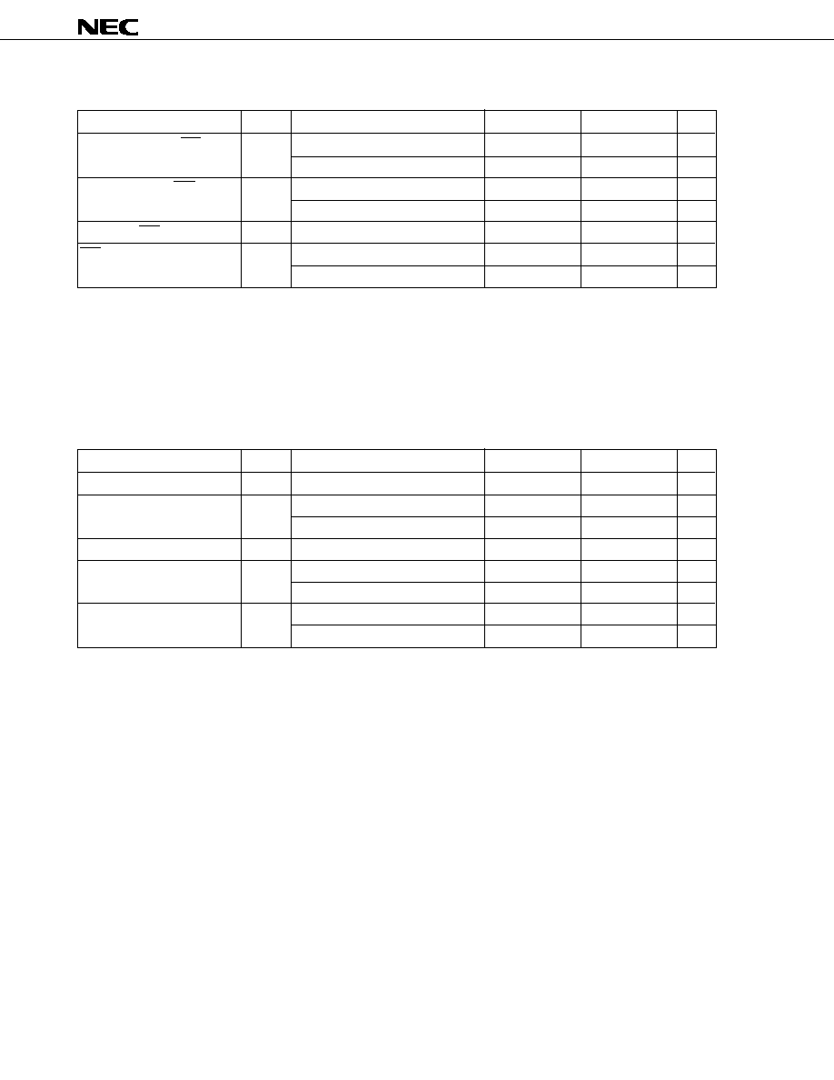
Item
Clock output
Watchdog timer
Standby
Interrupt
Supply voltage
Package
(2/2)
Functions
Selected from f
CLK
, f
CLK
/2, f
CLK
/4, f
CLK
/8, or f
CLK
/16 (can be used as a 1-bit output port)
1 channel
HALT/STOP/IDLE mode
24 (17 internal, 7 external (sampling clock variable input: 1))
BRK instruction, BRKCS instruction, operand error
1 internal, 1 external
16 internal, 6 external
∑
4-level programmable priority
∑
3 operation statuses: vectored interrupt, macro service, context switching
V
DD
= 2.7 to 5.5 V
80-pin plastic QFP (14
◊
14
◊
2.7 mm)
80-pin plastic QFP (14
◊
14
◊
1.4 mm)
80-pin plastic TQFP (fine pitch) (12
◊
12 mm)
80-pin ceramic WQFN (14
◊
14 mm)
Hardware source
Software source
Nonmaskable
Maskable

µ
PD78P4038Y
6
CONTENTS
1.
DIFFERENCES BETWEEN
µ
PD78P4038Y AND MASKED ROM PRODUCTS ....................
7
2.
PIN CONFIGURATION (TOP VIEW) .........................................................................................
8
3.
BLOCK DIAGRAM .....................................................................................................................
11
4.
LIST OF PIN FUNCTIONS .........................................................................................................
12
4.1
Pins for Normal Operating Mode .................................................................................................
12
4.2
Pins for PROM Programming Mode (V
PP
+5 V or +12.5 V, RESET = L) ..............................
15
4.2.1
Pin functions ..................................................................................................................
15
4.2.2
Pin functions ..................................................................................................................
16
4.3
I/O Circuits for Pins and Handling of Unused Pins ..................................................................
17
5.
INTERNAL MEMORY SWITCHING (IMS) REGISTER ............................................................
20
6.
PROM PROGRAMMING ............................................................................................................
21
6.1
Operation Mode ..............................................................................................................................
21
6.2
PROM Write Sequence ..................................................................................................................
23
6.3
PROM Read Sequence ..................................................................................................................
27
7.
ERASURE CHARACTERISTICS (
µ
PD78P4038YKK-T ONLY) ...............................................
28
8.
PROTECTIVE FILM COVERING THE ERASURE WINDOW (
µ
PD78P4038YKK-T ONLY) ..
28
9.
QUALITY .....................................................................................................................................
28
10. SCREENING ONE-TIME PROM PRODUCTS ..........................................................................
28
11. ELECTRICAL CHARACTERISTICS .........................................................................................
29
12. PACKAGE DRAWINGS .............................................................................................................
55
13. RECOMMENDED SOLDERING CONDITIONS ........................................................................
59
APPENDIX A DEVELOPMENT TOOLS ..........................................................................................
61
APPENDIX B CONVERSION SOCKET (EV-9200GC-80) AND CONVERSION ADAPTER
(TGK-080SDW)..........................................................................................................
64
APPENDIX C RELATED DOCUMENTS ..........................................................................................
67
µ
PD78P4038Y
7
1. DIFFERENCES BETWEEN
µ
PD78P4038Y AND MASKED ROM PRODUCTS
The
µ
PD78P4038Y is produced by replacing the masked ROM in the
µ
PD784035Y,
µ
PD784036Y,
µ
PD784037Y,
or
µ
PD784038Y with PROM to which data can be written. The functions of the
µ
PD78P4038Y are the same as those
of the
µ
PD784035Y,
µ
PD784036Y,
µ
PD784037Y, or
µ
PD784038Y except for the PROM specification such as writing
and verification, except that the PROM size can be changed to 48 K, 64 K, or 96 Kbytes, and except that the internal
RAM size can be changed to 2,048 or 3,584 bytes.
Table 1-1 shows the differences between these products.
Table 1-1. Differences between the
µ
PD78P4038Y and Masked ROM Products
Product Name
Item
Internal program
memory
Internal RAM
Package
µ
PD78P4038Y
∑
128-Kbyte
PROM
∑
Can be changed
to 48 K, 64 K, or
96 Kbytes by
IMS
∑
4,352-byte
internal RAM
∑
Can be changed
to 2,048 or 3,584
bytes by IMS
µ
PD784038Y
∑
128-Kbyte
masked ROM
∑
4,352-byte
internal RAM
µ
PD784037Y
∑
96-Kbyte
masked ROM
∑
3,584-byte
internal RAM
µ
PD784036Y
∑
64-Kbyte
masked ROM
µ
PD784035Y
∑
48-Kbyte
masked ROM
∑
2,048-byte internal RAM
∑
80-pin plastic QFP (14
◊
14
◊
2.7 mm)
∑
80-pin plastic QFP (14
◊
14
◊
1.4 mm)
∑
80-pin plastic TQFP (fine pitch) (12
◊
12 mm)
80-pin ceramic
WQFN
(14
◊
14 mm)
µ
PD78P4038Y
8
2. PIN CONFIGURATION (TOP VIEW)
(1) Normal operating mode
∑ 80-pin plastic QFP (14
◊
14
◊
2.7 mm)
µ
PD78P4038YGC-3B9,
µ
PD78P4038YGC-
◊◊◊
-3B9
∑ 80-pin plastic QFP (14
◊
14
◊
1.4 mm)
µ
PD78P4038YGC-8BT
∑ 80-pin plastic TQFP (fine pitch) (12
◊
12 mm)
µ
PD78P4038YGK-BE9,
µ
PD78P4038YGK-
◊◊◊
-BE9
∑ 80-pin ceramic WQFN (14
◊
14 mm)
µ
PD78P4038YKK-T
Note
Connect the TEST pin to V
SS0
directly.
60
59
58
57
56
55
54
53
52
51
50
49
48
47
46
45
44
43
42
41
21 22 23 24 25 26 27 28 29 30 31 32 33 34 35 36 37 38 39 40
80 79 78 77 76 75 74 73 72 71 70 69 68 67 66 65 64 63 62 61
P74/ANI4
P73/ANI3
P72/ANI2
P71/ANI1
P70/ANI0
V
DD0
P17
P16
P15
P14/T
X
D2/SO2
P13/R
X
D2/SI2
P12/ASCK2/SCK2
P11/PWM1
P10/PWM0
TEST
Note
V
SS0
ASTB/CLKOUT
P40/AD0
P41/AD1
P42/AD2
P32/SCK0/SCL
P33/SO0/SDA
P34/ TO0
P35/ TO1
P36/ TO2
P37/ TO3
RESET
V
DD1
X2
X1
V
SS1
P00
P01
P02
P03
P04
P05
P06
P07
P67/REFRQ/HLDAK
P66/
WAIT/HLDRQ
P65/
WR
P64
/RD
P63/A19
P62
/A18
P61/A17
P60/A16
P57/A15
P56/A14
P55/A13
P54
/A12
P53/A11
P52
/A10
P51/A9
P50/A8
P47/AD7
P46/AD6
P45/AD5
P44
/AD4
P43/AD3
P31/
TxD/SO1
P30/RxD/SI1
P27/SI0
P26/INTP5
P25/INTP4
/ASCK/SCK1
P24
/INTP3
P23/INTP2
/CI
P22
/INTP1
P21/INTP0
P20/NMI
AV
REF3
AV
REF2
ANO1
ANO0
AV
SS
AV
REF1
AV
DD
P77/ANI7
P76/ANI6
P75/ANI5
1
2
3
4
5
6
7
8
9
10
11
12
13
14
15
16
17
18
19
20

µ
PD78P4038Y
9
P60-P67
: Port 6
P70-P77
: Port 7
PWM0, PWM1 : Pulse width modulation output
RD
: Read strobe
REFRQ
: Refresh request
RESET
: Reset
RxD, RxD2
: Receive data
SCK0-SCK2
: Serial clock
SCL
: Serial clock
SDA
: Serial data
SI0-SI2
: Serial input
SO0-SO2
: Serial output
TEST
: Test
TO0-TO3
: Timer output
TxD, TxD2
: Transmit data
V
DD0
, V
DD1
: Power supply
V
SS0
, V
SS1
: Ground
WAIT
: Wait
WR
: Write strobe
X1, X2
: Crystal
A8-A19
: Address bus
AD0-AD7
: Address/data bus
ANI0-ANI7
: Analog input
ANO0, ANO1
: Analog output
ASCK, ASCK2 : Asynchronous serial clock
ASTB
: Address strobe
AV
DD
: Analog power supply
AV
REF1
-AV
REF3
: Reference voltage
AV
SS
: Analog ground
CI
: Clock input
CLKOUT
: Clock output
HLDAK
: Hold acknowledge
HLDRQ
: Hold request
INTP0-INTP5
: Interrupt from peripherals
NMI
: Non-maskable interrupt
P00-P07
: Port 0
P10-P17
: Port 1
P20-P27
: Port 2
P30-P37
: Port 3
P40-P47
: Port 4
P50-P57
: Port 5
µ
PD78P4038Y
10
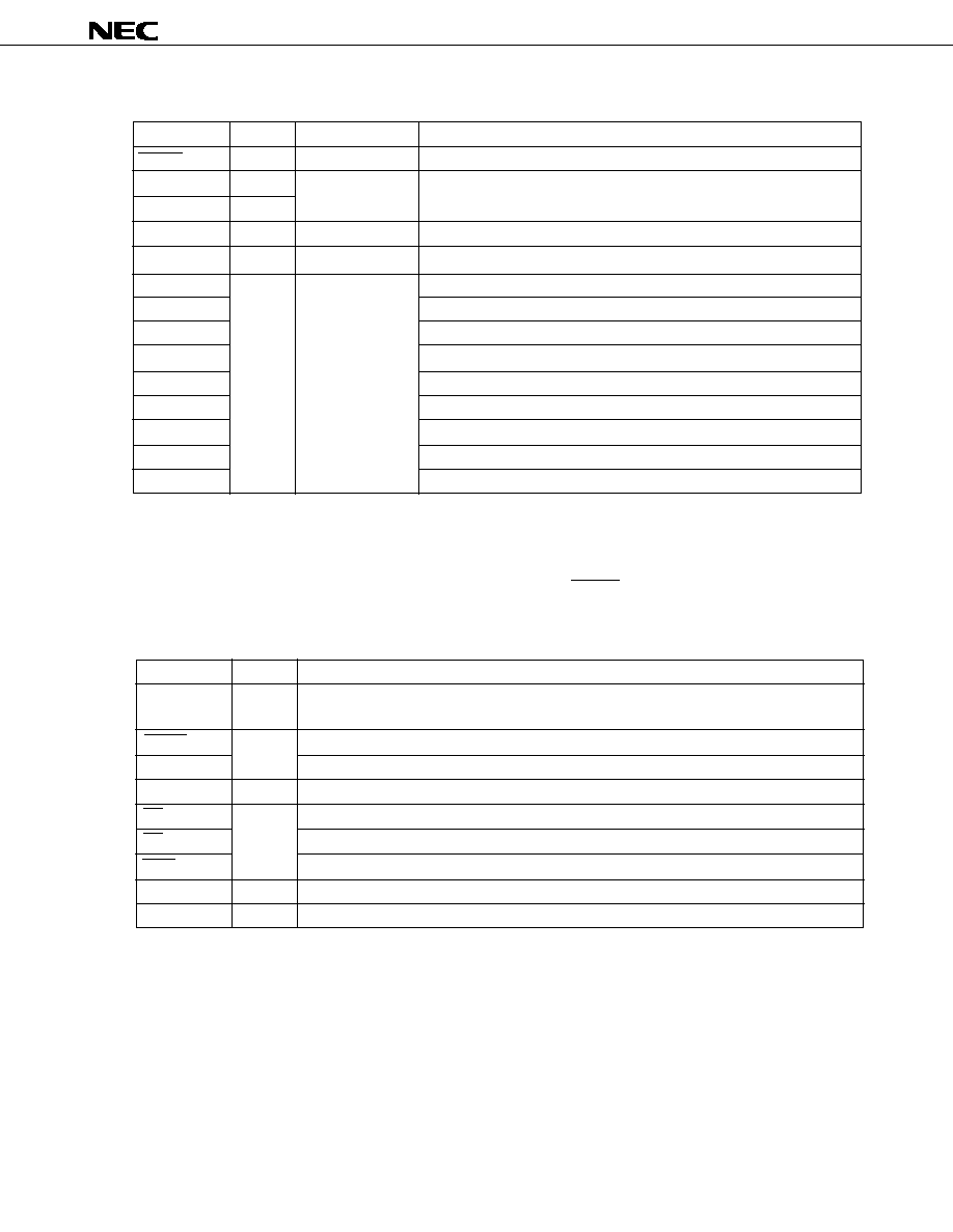
(2) PROM programming mode
∑ 80-pin plastic QFP (14
◊
14
◊
2.7 mm)
µ
PD78P4038YGC-3B9,
µ
PD78P4038YGC-
◊◊◊
-3B9
∑ 80-pin plastic QFP (14
◊
14
◊
1.4 mm)
µ
PD78P4038YGC-8BT
∑ 80-pin plastic TQFP (fine pitch) (12
◊
12 mm)
µ
PD78P4038YGK-BE9,
µ
PD78P4038YGK-
◊◊◊
-BE9
∑ 80-pin ceramic WQFN (14
◊
14 mm)
µ
PD78P4038YKK-T
Caution L
: Connect these pins separately to the V
SS
pins through 10-k
pull-down resistors.
V
SS
: To be connected to the ground.
Open : Nothing should be connected on these pins.
RESET: Set a low-level input.
A0-A16
: Address bus
RESET
: Reset
CE
: Chip enable
V
DD
: Power supply
D0-D7
: Data bus
V
PP
: Programming power supply
OE
: Output enable
V
SS
: Ground
PGM
: Program
60
59
58
57
56
55
54
53
52
51
50
49
48
47
46
45
44
43
42
41
21 22 23 24 25 26 27 28 29 30 31 32 33 34 35 36 37 38 39 40
80 79 78 77 76 75 74 73 72 71 70 69 68 67 66 65 64 63 62 61
V
PP
V
SS
Open
A0
A1
A2
RESET
V
DD
Open
(L)
V
SS
D0
D1
D2
D3
D4
D5
D6
D7
(L)
PGM
CE
OE
V
DD
1
2
3
4
5
6
7
8
9
10
11
12
13
14
15
16
17
18
19
20
A15
A14
A13
A12
A11
A10
A16
A8
A7
A6
A5
A4
A3
V
DD
(L)
(L)
V
SS
Open
Open
Open
V
SS
V
SS
A9
Open
Open
(L)
Open
µ
PD78P4038Y
11
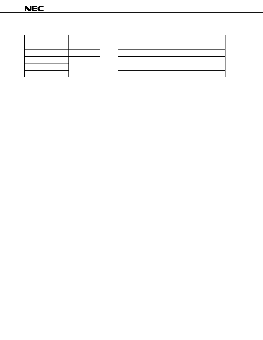
3. BLOCK DIAGRAM
Note
In the PROM programming mode.
NMI
INTP0-INTP5
INTP3
TO0
TO1
INTP0
INTP1
INTP2/CI
TO2
TO3
P00-P03
P04-P07
PWM0
PWM1
ANO0
ANO1
AV
REF2
AV
REF3
ANI0-ANI7
AV
DD
AV
REF1
AV
SS
INTP5
A/D
converter
D/A
converter
Real-time
output port
PWM
UART/IOE2
R
X
D/SI1
T
X
D/SO1
ASCK/SCK1
R
X
D2/SI2
T
X
D2/SO2
ASCK2/SCK2
SCK0/SCL
SO0/SDA
SI0
ASTB/CLKOUT
AD0-AD7
A8-A15
A16-A19
P20-P27
P30-P37
P40-P47
P50-P57
P60-P67
P70-P77
RESET
TEST
X1
X2
V
PP
Note
V
DD0
, V
DD1
V
SS0
, V
SS1
RD
WR
WAIT/HLDRQ
REFRQ/HLDAK
D0-D7
Note
A0-A16
Note
CE
Note
OE
Note
PGM
Note
P00-P07
P10-P17
Baud-rate
generator
Clock output
UART/IOE1
Bus
interface
Port 0
Port 1
Port 2
Port 3
Port 4
Port 5
Port 6
Port 7
System
control
Watchdog
timer
Baud-rate
generator
Clocked
serial
interface
Timer 3
(16 bits)
PROM
(128 Kbytes)
RAM
(3,840 bytes)
78 K/IV
CPU core
(RAM 512 bytes)
Timer/counter 2
(16 bits)
Timer/counter 1
(16 bits)
Timer/counter 0
(16 bits)
Programmable
interrupt
controller

µ
PD78P4038Y
12
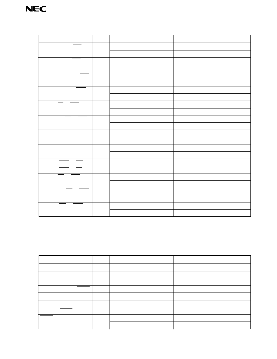
Pin
P00-P07
P10
P11
P12
P13
P14
P15-P17
P20
P21
P22
P23
P24
P25
P26
P27
P30
P31
P32
P33
P34-P37
P40-P47
I/O
I/O
I/O
Input
I/O
I/O
Alternate-Function
≠
PWM0
PWM1
ASCK2/SCK2
R
X
D2/SI2
T
X
D2/SO2
≠
NMI
INTP0
INTP1
INTP2/CI
INTP3
INTP4/ASCK/SCK1
INTP5
SI0
R
X
D/SI1
T
X
D/SO1
SCK0/SCL
SO0/SDA
TO0-TO3
AD0-AD7
Function
Port 0 (P0):
∑
8-bit I/O port.
∑
Functions as a real-time output port (4 bits
◊
2).
∑
Inputs and outputs can be specified bit by bit.
∑
The use of the pull-up resistors can be specified by software for the pins
in the input mode together.
∑
Can drive a transistor.
Port 1 (P1):
∑
8-bit I/O port.
∑
Inputs and outputs can be specified bit by bit.
∑
The use of the pull-up resistors can be specified by software for the pins
in the input mode together.
∑
Can drive LED.
Port 2 (P2):
∑
8-bit input-only port.
∑
P20 does not function as a general-purpose port (nonmaskable
interrupt). However, the input level can be checked by an interrupt
service routine.
∑
The use of the pull-up resistors can be specified by software for pins
P22 to P27 (in units of 6 bits).
∑
The P25/INTP4/ASCK/SCK1 pin functions as the SCK1 output pin by
CSIM1.
Port 3 (P3):
∑
8-bit I/O port.
∑
Inputs and outputs can be specified bit by bit.
∑
The use of the pull-up resistors can be specified by software for the pins
in the input mode together.
Port 4 (P4):
∑
8-bit I/O port.
∑
Inputs and outputs can be specified bit by bit.
∑
The use of the pull-up resistors can be specified by software for the pins
in the input mode together.
∑
Can drive LED.
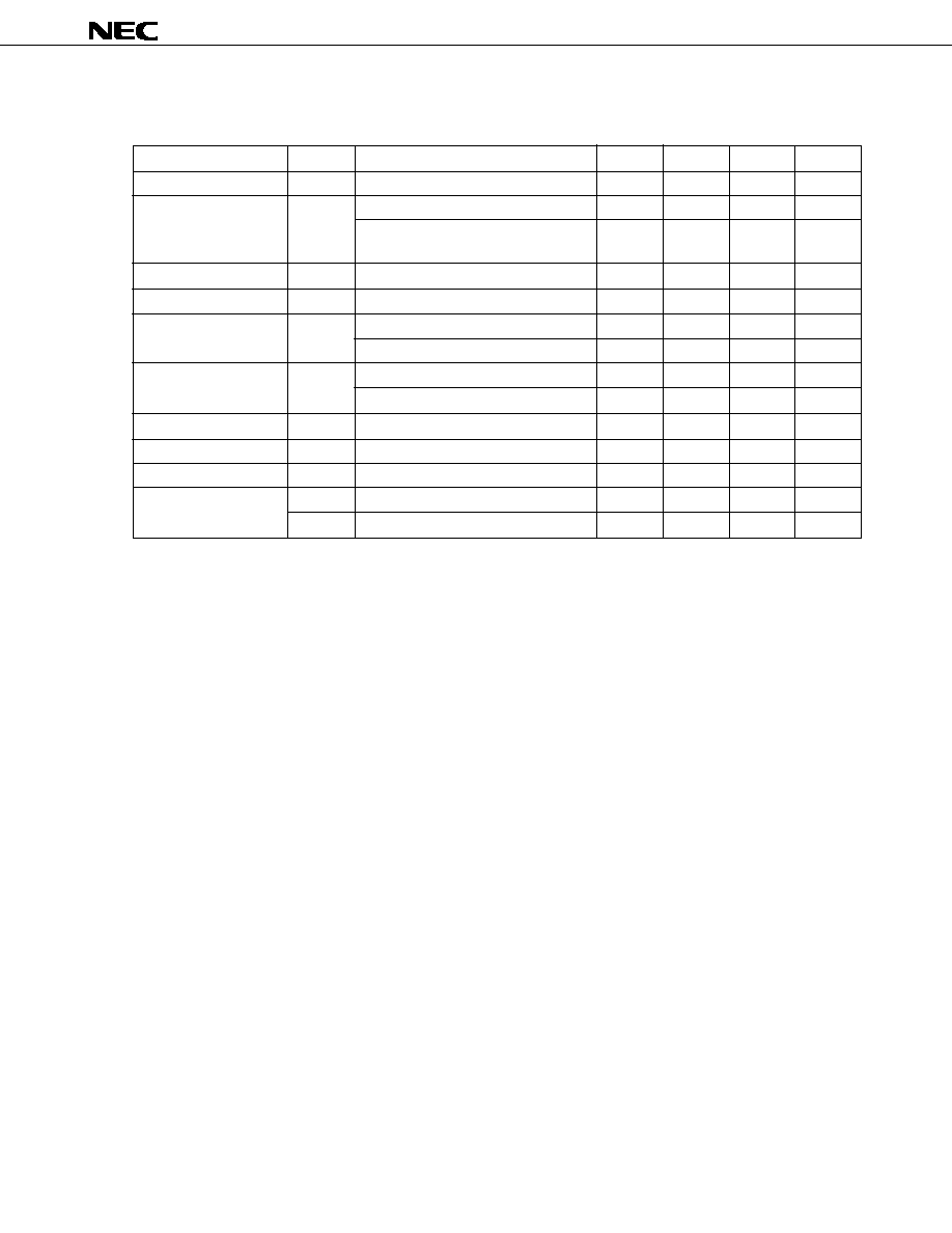
4. LIST OF PIN FUNCTIONS
4.1 Pins for Normal Operating Mode
(1) Port pins (1/2)
µ
PD78P4038Y
13
(1) Port pins (2/2)
Pin
P50-P57
P60-P63
P64
P65
P66
P67
P70-P77
I/O
I/O
I/O
I/O
Function
Port 5 (P5):
∑
8-bit I/O port.
∑
Inputs and outputs can be specified bit by bit.
∑
The use of the pull-up resistors can be specified by software for the pins
in the input mode together.
∑
Can drive LED.
Port 6 (P6):
∑
8-bit I/O port.
∑
Inputs and outputs can be specified bit by bit.
∑
The use of the pull-up resistors can be specified by software for the pins
in the input mode together.
Port 7 (P7):
∑
8-bit I/O port.
∑
Inputs and outputs can be specified bit by bit.
Alternate-Function
A8-A15
A16-A19
RD
WR
WAIT/HLDRQ
REFRQ/HLDAK
ANI0-ANI7
µ
PD78P4038Y
14
(2) Non-port pins (1/2)
Pin
TO0-TO3
CI
R
X
D
R
X
D2
T
X
D
T
X
D2
ASCK
ASCK2
SDA
SI0
SI1
SI2
SO0
SO1
SO2
SCK0
SCK1
SCK2
SCL
NMI
INTP0
INTP1
INTP2
INTP3
INTP4
INTP5
AD0-AD7
A8-A15
A16-A19
RD
WR
WAIT
REFRQ
HLDRQ
HLDAK
ASTB
CLKOUT
I/O
Output
Input
Input
Output
Input
I/O
Input
Output
I/O
Input
I/O
Output
Output
Output
Output
Input
Output
Input
Output
Output
Output
Function
Timer output
Input of a count clock for timer/counter 2
Serial data input (UART0)
Serial data input (UART2)
Serial data output (UART0)
Serial data output (UART2)
Baud rate clock input (UART0)
Baud rate clock input (UART2)
Serial data I/O (2-wire serial I/O, I
2
C bus)
Serial data input (3-wire serial I/O0)
Serial data input (3-wire serial I/O1)
Serial data input (3-wire serial I/O2)
Serial data output (3-wire serial I/O0)
Serial data output (3-wire serial I/O1)
Serial data output (3-wire serial I/O2)
Serial clock I/O (3-wire serial I/O0)
Serial clock I/O (3-wire serial I/O1)
Serial clock I/O (3-wire serial I/O2)
Serial clock I/O (2-wire serial I/O, I
2
C bus)
External interrupt request
≠
∑
Input of a count clock for timer/counter 1
∑
Capture/trigger signal for CR11 or CR12
∑
Input of a count clock for timer/counter 2
∑
Capture/trigger signal for CR22
∑
Input of a count clock for timer/counter 2
∑
Capture/trigger signal for CR21
∑
Input of a count clock for timer/counter 0
∑
Capture/trigger signal for CR02
≠
Input of a conversion start trigger for A/D converter
Time multiplexing address/data bus (for connecting external memory)
High-order address bus (for connecting external memory)
High-order address bus during address expansion (for connecting external memory)
Strobe signal output for reading the contents of external memory
Strobe signal output for writing on external memory
Wait signal insertion
Refresh pulse output to external pseudo static memory
Input of bus hold request
Output of bus hold response
Latch timing output of time multiplexing address (A0-A7) (for connecting
external memory)
Clock output
Alternate-Function
P34-P37
P23/INTP2
P30/SI1
P13/SI2
P31/SO1
P14/SO2
P25/INTP4/SCK1
P12/SCK2
P33/SO0
P27
P30/R
X
D
P13/R
X
D2
P33/SDA
P31/T
X
D
P14/T
X
D2
P32/SCL
P25/INTP4/ASCK
P12/ASCK2
P32/SCK0
P20
P21
P22
P23/CI
P24
P25/ASCK/SCK1
P26
P40-P47
P50-P57
P60-P63
P64
P65
P66/HLDRQ
P67/HLDAK
P66/WAIT
P67/REFRQ
CLKOUT
ASTB
µ
PD78P4038Y
15
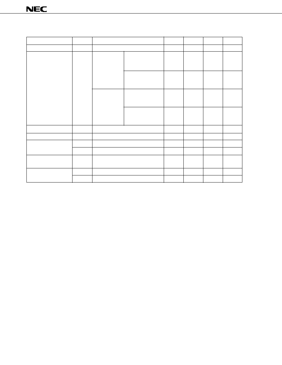
(2) Non-port pins (2/2)
Pin
RESET
X1
X2
ANI0-ANI7
ANO0, ANO1
AV
REF1
AV
REF2
, AV
REF3
AV
DD
AV
SS
V
DD0
Note 1
V
DD1
Note 1
V
SS0
Note 2
V
SS1
Note 2
TEST
I/O
Input
Input
≠
Input
Output
≠
Function
Chip reset
Crystal input for system clock oscillation (A clock pulse can also be input
to the X1 pin.)
Analog voltage inputs for the A/D converter
Analog voltage inputs for the D/A converter
Application of A/D converter reference voltage
Application of D/A converter reference voltage
Positive power supply for the A/D converter
Ground for the A/D converter
Positive power supply of the port part
Positive power supply except for the port part
Ground of the port part
Ground except for the port part
Directly connect to V
SS0
. (The TEST pin is for the IC test.)
Alternate-Function
≠
≠
P70-P77
≠
≠
Pin Name
V
PP
RESET
A0-A16
D0-D7
CE
OE
PGM
V
DD
V
SS
I/O
≠
Input
I/O
Input
≠
≠
Function
PROM programming mode selection
High voltage input during program write or verification
PROM programming mode selection
Address bus
Data bus
PROM enable input/program pulse input
Read strobe input to PROM
Program/program inhibit input during PROM programming mode
Positive power supply
GND
Notes 1. The potential of the V
DD0
pin must be equal to that of the V
DD1
pin.
2. The potential of the V
SS0
pin must be equal to that of the V
SS1
pin.
4.2 Pins for PROM Programming Mode (V
PP
+5 V or +12.5 V, RESET = L)
4.2.1 Pin functions

µ
PD78P4038Y
16
4.2.2 Pin functions
(1) V
PP
(Programming power supply): Input
Input pin for setting the
µ
PD78P4038Y to the PROM programming mode. When the input voltage on this pin
is +5 V or more and when RESET input goes low, the
µ
PD78P4038Y enters the PROM programming mode.
When CE is made low for V
PP
= +12.5 V and OE = high, program data on D0 to D7 can be written into the internal
PROM cell selected by A0 to A16.
(2) RESET (Reset): Input
Input pin for setting the
µ
PD78P4038Y to the PROM programming mode. When input on this pin is low, and
when the input voltage on the V
PP
pin goes +5 V or more, the
µ
PD78P4038Y enters the PROM programming
mode.
(3) A0 to A16 (Address bus): Input
Address bus that selects an internal PROM address (0000H to 1FFFFH)
(4) D0 to D7 (Data bus): I/O
Data bus through which a program is written on or read from internal PROM
(5) CE (Chip enable): Input
This pin inputs the enable signal from internal PROM. When this signal is active, a program can be written or
read.
(6) OE (Output enable): Input
This pin inputs the read strobe signal to internal PROM. When this signal is made active for CE = low, a one-
byte program in the internal PROM cell selected by A0 to A16 can be read onto D0 to D7.
(7) PGM (Program): Input
The input pin for the operation mode control signal of the internal PROM.
Upon activation, writing to the internal PROM is enabled.
Upon inactivation, reading from the internal PROM is enabled.
(8) V
DD
Positive power supply pin
(9) V
SS
Ground potential pin

µ
PD78P4038Y
17
4.3 I/O Circuits for Pins and Handling of Unused Pins
Table 4-1 describes the types of I/O circuits for pins and the handling of unused pins.
Figure 4-1 shows the configuration of these various types of I/O circuits.
Table 4-1. Types of I/O Circuits for Pins and Handling of Unused Pins (1/2)
Pin
P00-P07
P10/PWM0
P11/PWM1
P12/ASCK2/SCK2
P13/R
X
D2/SI2
P14/T
X
D2/SO2
P15-P17
P20/NMI
P21/INTP0
P22/INTP1
P23/INTP2/CI
P24/INTP3
P25/INTP4/ASCK/SCK1
P26/INTP5
P27/SI0
P30/R
X
D/SI1
P31/T
X
D/SO1
P32/SCK0/SCL
P33/SO0/SDA
P34/TO0-P37/TO3
P40/AD0-P47/AD7
P50/A8-P57/A15
P60/A16-P63/A19
P64/RD
P65/WR
P66/WAIT/HLDRQ
P67/REFRQ/HLDAK
P70/ANI0-P77/ANI7
ANO0, ANO1
ASTB/CLKOUT
Recommended Connection Method for Unused Pins
Input state:
To be connected to V
DD0
Output state: To be left open
To be connected to V
DD0
or V
SS0
To be connected to V
DD0
Input state:
To be connected to V
DD0
Output state: To be left open
To be connected to V
DD0
Input state:
To be connected to V
DD0
Output state: To be left open
Input state:
To be connected to V
DD0
or V
SS0
Output state: To be left open
To be left open
I/O Circuit Type
5-H
8-C
5-H
2
2-C
8-C
2-C
5-H
10-B
5-H
20-A
12
4-B
I/O
I/O
Input
I/O
Input
I/O
I/O
Output
µ
PD78P4038Y
18
Table 4-1. Types of I/O Circuits for Pins and Handling of Unused Pins (2/2)
Caution When the I/O mode of an I/O alternate-function pin is unpredictable, connect the pin to V
DD0
through a resistor of 10 to 100 kilohms (particularly when the voltage of the reset input pin
becomes higher than that of the low level input at power-on or when I/O is switched by software).
Remark Since type numbers are consistent in the 78K Series, those numbers are not always serial in each
product. (Some circuits are not included.)
Recommended Connection Method for Unused Pins
≠
To be connected to V
SS0
directly
To be connected to V
SS0
To be connected to V
DD0
I/O
Input
Pin
RESET
TEST
AV
REF1
-AV
REF3
AV
SS
AV
DD
I/O Circuit Type
2
1-A
≠
µ
PD78P4038Y
19
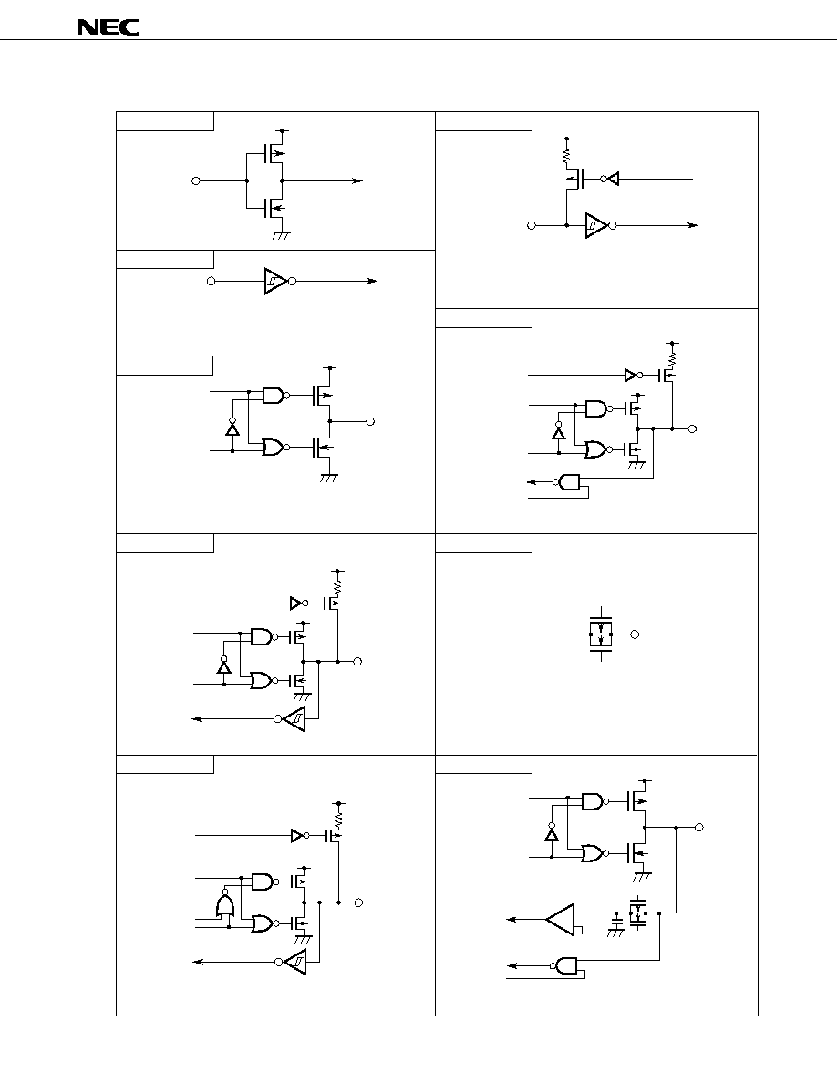
Figure 4-1. I/O Circuits for Pins
Type 1-A
Type 2-C
Type 2
Type 4-B
Type 8-C
Type 10-B
Type 5-H
Type 12
Type 20-A
IN
V
DD0
V
SS0
P
N
IN
Schmitt trigger input with hysteresis characteristics
Schmitt trigger input with hysteresis characteristics
IN
V
DD0
P
Pull-up
enable
Data
V
DD0
V
SS0
P
N
OUT
Output
disable
Push-pull output which can output high impedance
(both the positive and negative channels are off.)
Data
V
DD0
V
SS0
P
N
IN/OUT
Output
disable
V
DD0
P
Pull-up
enable
Input
enable
Data
V
DD0
V
SS0
P
N
IN/OUT
Output
disable
V
DD0
P
Pull-up
enable
N
P
Analog output
voltage
OUT
Data
V
DD0
V
SS0
P
N
IN/OUT
Output
disable
V
DD0
P
Pull-up
enable
Open
drain
Data
Comparator
V
DD0
V
SS0
AV
REF
AV
SS
P
(Threshold voltage)
P
N
N
IN/OUT
Output
disable
Input
enable
+
≠
µ
PD78P4038Y
20
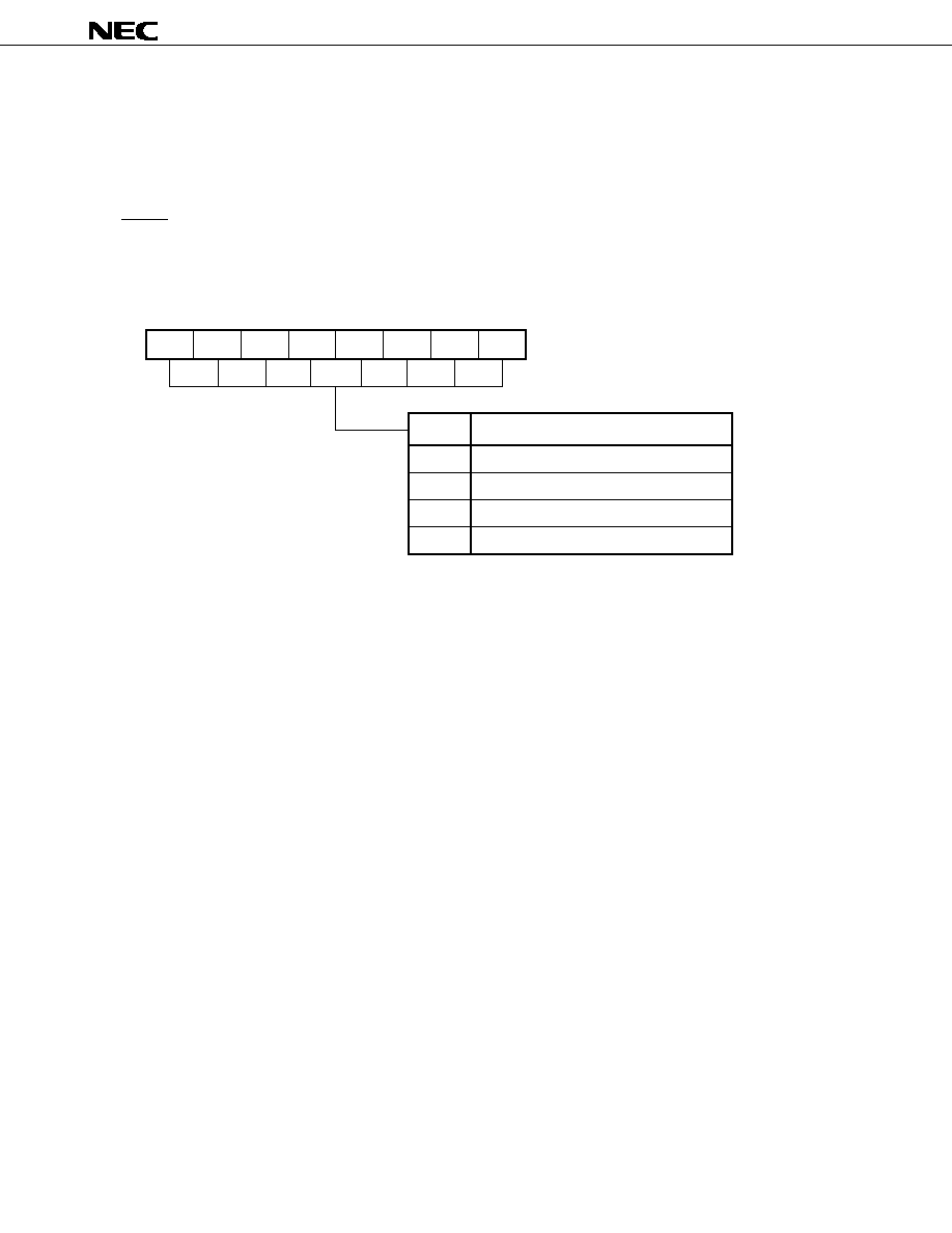
5. INTERNAL MEMORY SWITCHING (IMS) REGISTER
This register enables the software to avoid using part of the internal memory. The IMS register can be set to
establish the same memory mapping as used in ROM products that have different internal memory (ROM and RAM)
configurations.
The IMS register is set using 8-bit memory operation instructions.
A RESET input sets the IMS register to FFH.
Figure 5-1. Internal Memory Switching (IMS) Register
The IMS is not contained in a mask ROM product (
µ
PD784035Y,
µ
PD784036Y,
µ
PD784037Y, or
µ
PD784038Y).
But the action is not affected if the write command to the IMS is executed to the mask ROM product.
IMS
IMS7
IMS6
IMS5
IMS4
IMS3
IMS2
IMS1
IMS0
7
6
5
4
3
2
1
0
0FFFCH
Address
FFH
After Reset
W
R/W
IMS0-7
FFH
EEH
DCH
Same as the PD784038Y
Memory Size
CCH
µ
Same as the PD784037Y
µ
Same as the PD784036Y
µ
Same as the PD784035Y
µ
µ
PD78P4038Y
21
6. PROM PROGRAMMING
The
µ
PD78P4038Y has an on-chip 128-KB PROM device for use as program memory. When programming, set
the V
PP
and RESET pins for PROM programming mode. See (2) in Chapter 2 with regard to handling of other, unused
pins.
6.1 Operation Mode
PROM programming mode is selected when +5 V or +12.5 V is added to the V
PP
pin or low-level input is added
to the RESET pin. This mode can be set to operation mode by setting the CE pin, OE pin, and PGM pin as shown
in Table 6-1 below.
In addition, the PROM contents can be read by setting read mode.
Table 6-1. PROM Programming Operation Mode
Pin
RESET
V
PP
V
DD
CE
OE
PGM
D0-D7
Operation Mode
Page data latch
L
+12.5 V
+6.5 V
H
L
H
Data input
Page write
H
H
L
High impedance
Byte write
L
H
L
Data input
Program verify
L
L
H
Data output
Program inhibit
◊
H
H
High impedance
◊
L
L
Read
+5 V
+5 V
L
L
H
Data output
Output disable
L
H
◊
High impedance
Standby
H
◊
◊
High impedance
Remark
◊
= L or H

µ
PD78P4038Y
22
(1) Read mode
Set CE to L and OE to L to set read mode.
(2) Output disable mode
Set OE to H to set high impedance for data output and output disable mode.
Consequently, if several
µ
PD78P4038Y devices are connected to a data bus, the OE pins can be controlled to
select data output from any of the devices.
(3) Standby mode
Set CE to H to set standby mode.
In this mode, data output is set to high impedance regardless of the OE setting.
(4) Page data latch mode
At the beginning of page write mode, set CE to H, PGM to H, and OE to L to set page data latch mode.
In this mode, 1 page (4 bytes) of data are latched to the internal address/data latch circuit.
(5) Page write mode
After latching the address and data for one page (4 bytes) using page data latch mode, adding a 0.1 ms program
pulse (active, low) to the PGM pin with both CE and OE set to H causes page write to be executed. Later, setting
both CE and OE to L causes program verification to be executed.
If programming is not completed after one program pulse, the write and verify operations may be repeated X times
(where X
10).
(6) Byte write mode
Adding a 0.1 ms program pulse (active, low) to the PGM pin with both CE and OE set to H causes byte write
to be executed. Later, setting OE to L causes program verification to be executed.
If programming is not completed after one program pulse, the write and verify operations may be repeated X times
(where X
10).
(7) Program verify mode
Set CE to L, PGM to H, and OE to L to set program verify mode. Use verify mode for verification following each
write operation.
(8) Program inhibit mode
Program inhibit mode is used to write to a single device when several
µ
PD78P4038Y devices are connected in
parallel to OE , V
PP
, and D0 to D7 pins.
Use the page write mode or byte write mode described above for each write operation. Write operations cannot
be done for devices in which the PGM pin has been set to H.

µ
PD78P4038Y
23
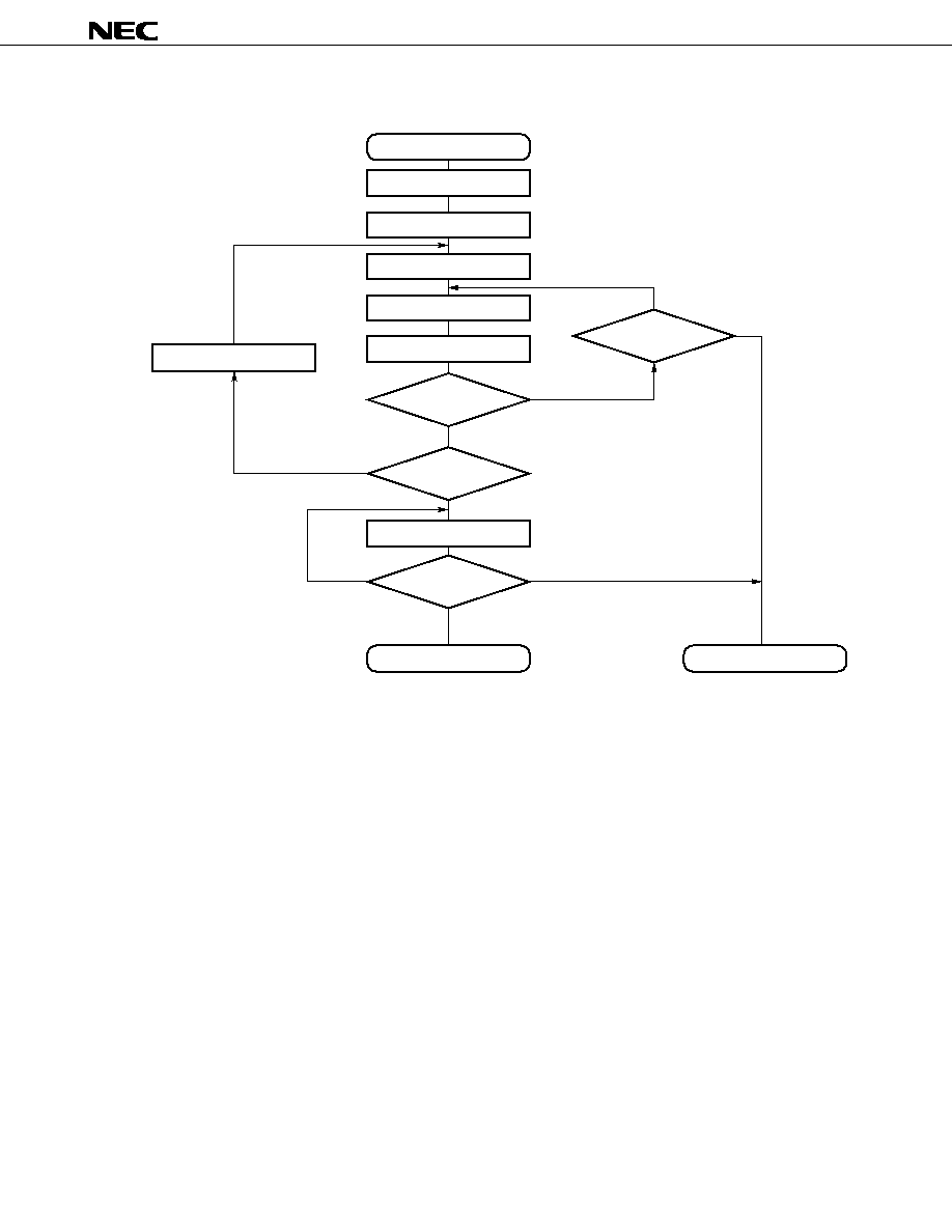
6.2 PROM Write Sequence
Figure 6-1. Page Program Mode Flowchart
Remark G = Start address
N = Program end address
Start
Address = G
V
DD
= +6.5 V, V
PP
= +12.5 V
X = 0
Latch
Address = Address + 1
Latch
Address = Address + 1
Latch
Address = Address + 1
0.1 ms program pulse
X = X + 1
Latch
No
X = 10 ?
Yes
Verify 4 bytes
Pass
Address = N ?
Yes
V
DD
= 4.5-5.5 V, V
PP
= V
DD
Verify all bytes
Pass
No
All pass
Write end
Fail
Defective
Address = Address + 1
Fail
µ
PD78P4038Y
24
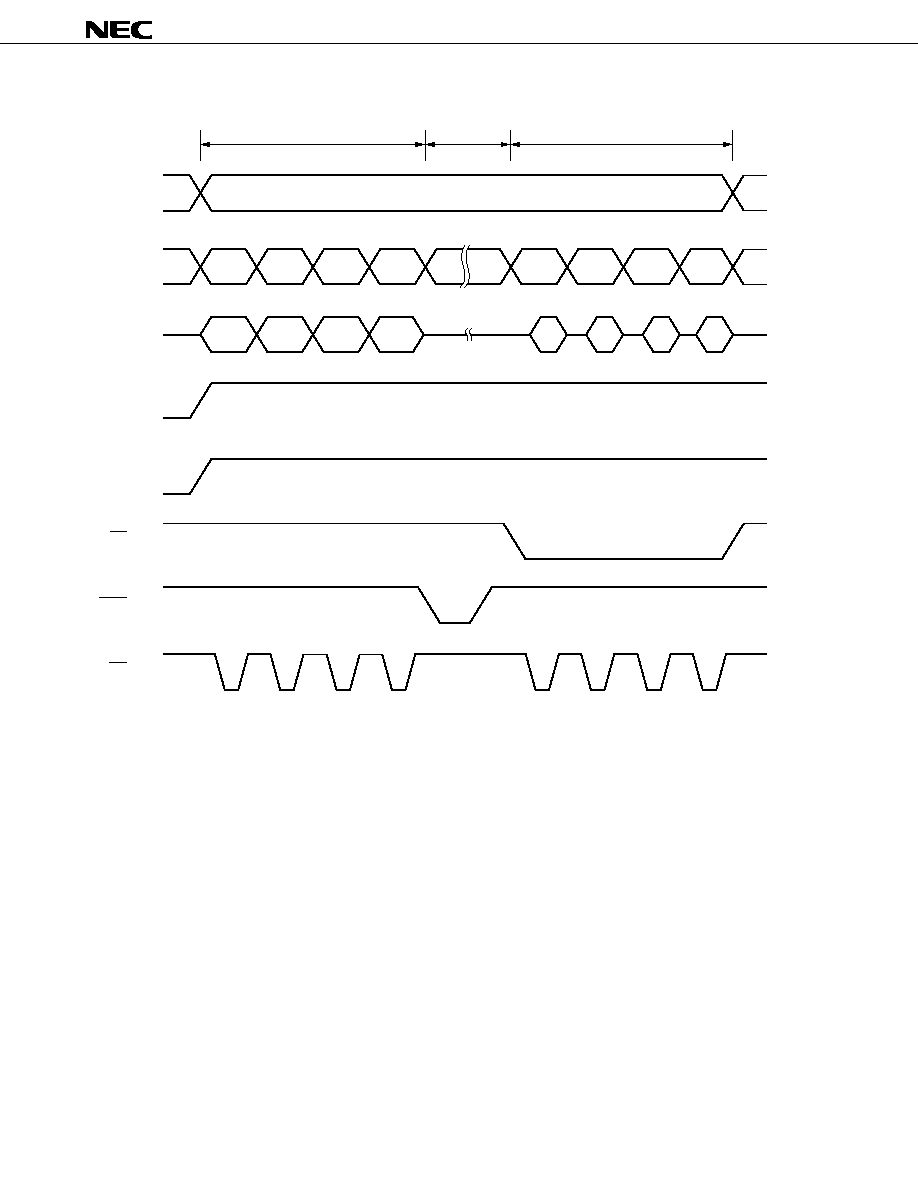
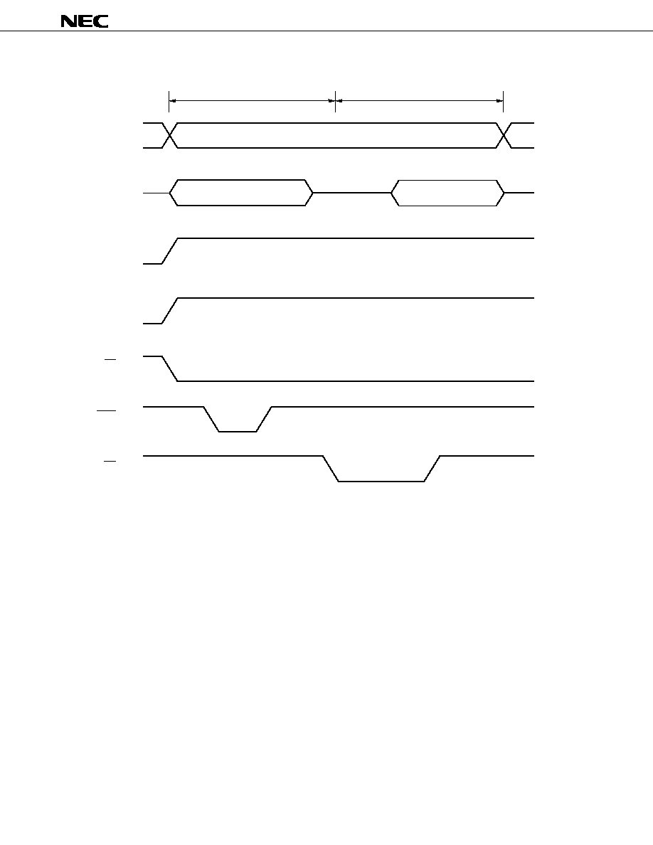
Figure 6-2. Page Program Mode Timing
Page data latch
Page program
Program verify
Data input
Data output
A2-A16
A0, A1
D0-D7
V
PP
V
DD
V
PP
V
DD
+1.5
V
DD
V
IH
V
IL
OE
V
IH
V
IL
PGM
V
IH
V
IL
CE
V
DD
µ
PD78P4038Y
25
Figure 6-3. Byte Program Mode Flowchart
Remark G = Start address
N = Program end address
Start
Address = G
V
DD
= +6.5 V, V
PP
= +12.5 V
X
= 0
X
= X + 1
0.1 ms program pulse
Verify
Address = N ?
Write end
Defective
Verify all bytes
V
DD
= 4.5-5.5 V, V
PP
= V
DD
Address = Address + 1
Fail
Pass
Fail
All pass
Yes
X
= 10 ?
No
Yes
Pass
No
µ
PD78P4038Y
26
Figure 6-4. Byte Program Mode Timing
Cautions 1. Add V
DD
before V
PP
, and turn off the V
DD
after V
PP
.
2. Do not allow V
PP
to exceed +13.5 V including overshoot.
3. Reliability problems may result if the device is inserted or pulled out while +12.5 V is applied
at V
PP
.
Program
Program verify
Data input
Data output
A0-A16
D0-D7
V
PP
V
DD
V
PP
V
DD
+1.5
V
DD
V
DD
V
IH
V
IL
CE
V
IH
V
IL
PGM
V
IH
V
IL
OE
µ
PD78P4038Y
27
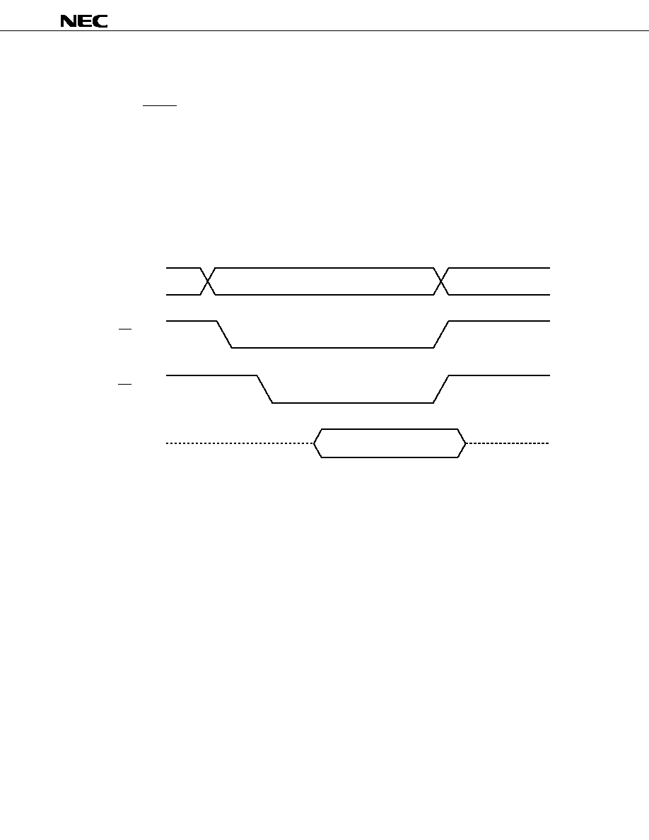
6.3 PROM Read Sequence
Follow this sequence to read the PROM contents to an external data bus (D0 to D7).
(1) Set the RESET pin to low level and add +5 V to the V
PP
pin. See (2) in Chapter 2 with regard to handling of
other, unused pins.
(2) Add +5 V to the V
DD
and V
PP
pins.
(3) Input the data address to be read to pins A0 to A16.
(4) Set read mode.
(5) Output the data to pins D0 to D7.
Figure 6-5 shows the timing of steps (2) to (5) above.
Figure 6-5. PROM Read Timing
Address input
Data output
CE (input)
A0-A16
OE (input)
D0-D7
Hi-Z
Hi-Z

µ
PD78P4038Y
28
7. ERASURE CHARACTERISTICS (
µ
PD78P4038YKK-T ONLY)
Data written in the
µ
PD78P4038YKK-T program memory can be erased (FFH); therefore users can write other
data in the memory.
To erase the written data, expose the erasure window to light with a wavelength shorter than approx. 400 nm. Normally,
ultraviolet light with a wavelength of 254 nm is employed. The amount of light required to completely erase the data
is as follows:
∑ Intensity of ultraviolet light
◊
erasing time: 57.6 W∑s/cm
2
min.
∑ Erasing time: About 80 minutes (When using a 12,000
µ
W/cm
2
ultraviolet lamp. It may, however, take more time
due to lamp deterioration, dirt on the erasure window, or the like.)
The ultraviolet lamp should be placed within 2.5 cm from the erasure window during erasure. In addition, if a filter
is attached to the ultraviolet lamp, remove the filter before erasure.
8. PROTECTIVE FILM COVERING THE ERASURE WINDOW (
µ
PD78P4038YKK-T ONLY)
To prevent EPROM from being erased inadvertently by light other than that from the lamp used for erasing EPROM,
or to prevent the internal circuits other than EPROM from malfunctioning by light, stick a protective film on the erasure
window except when EPROM is to be erased.
9. QUALITY
The
µ
PD78P4038YKK-T is not intended for use in mass-produced products; they do not have reliability high enough
for such purposes. Their use should be restricted to functional evaluation in experiment or trial manufacture.
10. SCREENING ONE-TIME PROM PRODUCTS
NEC cannot execute a complete test of one-time PROM products (
µ
PD78P4038YGC-3B9,
µ
PD78P4038YGC-
8BT, and
µ
PD78P4038YGK-BE9) due to their structure before shipment. It is recommended that you screen (verify)
PROM products after writing necessary data into them and storing them at 125
∞
C for 24 hours.
µ
PD78P4038Y
29
11. ELECTRICAL CHARACTERISTICS
ABSOLUTE MAXIMUM RATINGS (T
A
= 25
∞
C)
Caution Absolute maximum ratings are rated values beyond which physical damage will be caused to the
product; if the rated value of any of the parameters in the above table is exceeded, even
momentarily, the quality of the product may deteriorate. Always use the product within its rated
values.
D/A converter reference input
voltage
Parameter
Symbol
Conditions
Rating
Unit
Supply voltage
V
DD
≠0.5 to +7.0
V
AV
DD
AV
SS
to V
DD
+ 0.5
V
AV
SS
≠0.5 to +0.5
V
Input voltage
V
I1
≠0.5 to V
DD
+ 0.5
V
V
I2
TEST/V
PP
pin and
≠0.5 to +13.5
V
P21/INTP0/A9 pin in PROM
programming mode
Output voltage
V
O
≠0.5 to V
DD
+ 0.5
V
Output low current
I
OL
At one pin
15
mA
Total of all output pins
100
mA
Output high current
I
OH
At one pin
≠10
mA
Total of all output pins
≠100
mA
A/D converter reference input
AV
REF1
≠0.5 to V
DD
+ 0.3
V
voltage
AV
REF2
≠0.5 to V
DD
+ 0.3
V
AV
REF3
≠0.5 to V
DD
+ 0.3
V
Operating ambient temperature
T
A
≠40 to +85
∞
C
Storage temperature
T
stg
≠65 to +150
∞
C
µ
PD78P4038Y
30
OPERATING CONDITIONS
∑ Operating ambient temperature (T
A
)
: ≠40 to +85
∞
C
∑ Rise time and fall time (t
r
, t
f
) (at pins which are not specified) : 0 to 200
µ
s
∑ Power supply voltage and clock cycle time
: See Figure 11-1.
Figure 11-1. Power Supply Voltage and Clock Cycle Time
CAPACITANCE (T
A
= 25
∞
C, V
DD
= V
SS
= 0 V)
Parameter
Input capacitance
Output capacitance
I/O capacitance
Symbol
C
I
C
O
C
IO
Conditions
f = 1 MHz
0 V on pins other than measured pins
MIN.
TYP.
MAX.
10
10
10
Unit
pF
pF
pF
10,000
4,000
1,000
125
100
62.5
10
0
1
2
3
4
5
6
7
Guaranteed
operating
range
Power supply voltage [V]
Clock cycle time t
CYK
[ns]

µ
PD78P4038Y
31
OSCILLATOR CHARACTERISTICS (T
A
= ≠40 to +85
∞
C, V
DD
= +4.5 to 5.5 V, V
SS
= 0 V)
Caution When using the system clock generator, run wires in the portion surrounded by broken lines
according to the following rules to avoid effects such as stray capacitance:
∑ Minimize the wiring.
∑ Never cause the wires to cross other signal lines.
∑ Never cause the wires to run near a line carrying a large varying current.
∑ Cause the grounding point of the capacitor of the oscillator circuit to have the same potential
as V
SS1
. Never connect the capacitor to a ground pattern carrying a large current.
∑ Never extract a signal from the oscillator.
Resonator
Ceramic resonator
or crystal
External clock
Recommended Circuit
Parameter
Oscillator frequency (f
XX
)
X1 input frequency (f
X
)
X1 input rise and fall times
(t
XR
, t
XF
)
X1 input high-level and low-
level widths (t
WXH
, t
WXL
)
MIN.
4
4
0
10
MAX.
32
32
10
125
Unit
MHz
MHz
ns
ns
V
SS1
X1
X2
C2
C1
X1
X2
HCMOS
inverter
µ
PD78P4038Y
32
OSCILLATOR CHARACTERISTICS (T
A
= ≠40 to +85
∞
C, V
DD
= +2.7 to 5.5 V, V
SS
= 0 V)
Caution When using the system clock generator, run wires in the portion surrounded by broken lines
according to the following rules to avoid effects such as stray capacitance:
∑
Minimize the wiring.
∑
Never cause the wires to cross other signal lines.
∑
Never cause the wires to run near a line carrying a large varying current.
∑
Cause the grounding point of the capacitor of the oscillator circuit to have the same potential
as V
SS1
. Never connect the capacitor to a ground pattern carrying a large current.
∑
Never extract a signal from the oscillator.
Resonator
Ceramic resonator
or crystal
External clock
Recommended Circuit
Parameter
Oscillator frequency (f
XX
)
X1 input frequency (f
X
)
X1 input rise and fall times
(t
XR
, t
XF
)
X1 input high-level and low-
level widths (t
WXH
, t
WXL
)
MIN.
4
4
0
10
MAX.
16
16
10
125
Unit
MHz
MHz
ns
ns
V
SS1
X1
X2
C2
C1
X1
X2
HCMOS
inverter
µ
PD78P4038Y
33
DC CHARACTERISTICS (T
A
= ≠40 to +85
∞
C, V
DD
= AV
DD
= +2.7 to 5.5 V, V
SS
= AV
SS
= 0 V) (1/2)
Notes 1. X1, X2, RESET, P12/ASCK2/SCK2, P20/NMI, P21/INTP0, P22/INTP1, P23/INTP2/CI, P24/INTP3,
P25/INTP4/ASCK/SCK1, P26/INTP5, P27/SI0, TEST
2. P40/AD0 to P47/AD7, P50/A8 to P57/A15
3. P60/A16 to P63/A19, P64/RD, P65/WR, P66/WAIT/HLDRQ, P67/REFRQ/HLDAK
4. P00 to P07
5. P10 to P17
6. P32/SCK0/SCL, P33/SO0/SDA
Parameter
Input low voltage
Input high voltage
Output low voltage
Output high voltage
X1 input low current
X1 input high current
Symbol
V
IL1
V
IL2
V
IL3
V
IH1
V
IH2
V
IH3
V
OL1
V
OL2
V
OL3
V
OH1
V
OH2
I
IL
I
IH
Conditions
For pins other than those described in
Notes 1, 2, 3, 4, and 6
For pins described in Notes 1, 2, 3, 4,
and 6
V
DD
= +5.0 V
±
10%
For pins described in Notes 2, 3, and 4
For pins other than those described in
Notes 1 and 6
For pins described in Notes 1 and 6
V
DD
= +5.0 V
±
10%
For pins described in Notes 2, 3, and 4
I
OL
= 2 mA
For pins other than those described in
Note 6
I
OL
= 3 mA
For pins described in Note 6
I
OL
= 6 mA
For pins described in Note 6
V
DD
= +5.0 V
±
10%
I
OL
= 8 mA
For pins described in Notes 2 and 5
I
OH
= ≠2 mA
V
DD
= +5.0 V
±
10%
I
OH
= ≠5 mA
For pins described in Note 4
EXTC = 0
0 V
V
I
V
IL2
EXTC = 0
V
IH2
V
I
V
DD
MIN.
≠0.3
≠0.3
≠0.3
0.7V
DD
0.8V
DD
2.2
V
DD
≠ 1.0
V
DD
≠ 1.4
TYP.
MAX.
0.3V
DD
0.2V
DD
+0.8
V
DD
+ 0.3
V
DD
+ 0.3
V
DD
+ 0.3
0.4
0.4
0.6
1.0
≠30
+30
Unit
V
V
V
V
V
V
V
V
V
V
V
V
µ
A
µ
A
µ
PD78P4038Y
34
DC CHARACTERISTICS (T
A
= ≠40 to +85
∞
C, V
DD
= AV
DD
= +2.7 to 5.5 V, V
SS
= AV
SS
= 0 V) (2/2)
Parameter
Input leakage current
Output leakage current
V
DD
supply current
Pull-up resistor
Symbol
I
L|
I
LO
I
DD1
I
DD2
I
DD3
R
L
Conditions
0 V
V
I
V
DD
For pins other than X1 when EXTC = 0
0 V
V
O
V
DD
Operation mode
f
XX
= 32 MHz
V
DD
= +5.0 V
±
10%
f
XX
= 16 MHz
V
DD
= +2.7 to 3.3 V
HALT mode
f
XX
= 32 MHz
V
DD
= +5.0 V
±
10%
f
XX
= 16 MHz
V
DD
= +2.7 to 3.3 V
IDLE mode
f
XX
= 32 MHz
(EXTC = 0)
V
DD
= +5.0 V
±
10%
f
XX
= 16 MHz
V
DD
= +2.7 to 3.3 V
V
I
= 0 V
MIN.
15
TYP.
25
12
13
8
MAX.
±
10
±
10
45
25
26
12
12
8
80
Unit
µ
A
µ
A
mA
mA
mA
mA
mA
mA
k
µ
PD78P4038Y
35
AC CHARACTERISTICS (T
A
= ≠40 to +85
∞
C, V
DD
= AV
DD
= +2.7 to 5.5 V, V
SS
= AV
SS
= 0 V)
(1) Read/write operation (1/2)
Remarks T:
t
CYK
(system clock cycle time)
a:
1 (during address wait), otherwise, 0
n:
Number of wait states (n
0)
Unit
ns
ns
ns
ns
ns
ns
ns
ns
ns
ns
ns
ns
ns
ns
ns
ns
ns
ns
ns
ns
ns
ns
ns
ns
ns
ns
ns
ns
ns
ns
ns
ns
Parameter
Address setup time
ASTB high-level width
Address hold time (to ASTB
)
Address hold time (to RD
)
Delay from address to RD
Address float time (to RD
)
Delay from address to data input
Delay from ASTB
to data input
Delay from RD
to data input
Delay from ASTB
to RD
Data hold time (to RD
)
Delay from RD
to address active
Delay from RD
to ASTB
RD low-level width
Address hold time (to WR
)
Delay from address to WR
Delay from ASTB
to data output
Delay from WR
to data output
Delay from ASTB
to WR
Symbol
t
SAST
t
WSTH
t
HSTLA
t
HRA
t
DAR
t
FRA
t
DAID
t
DSTID
t
DRID
t
DSTR
t
HRID
t
DRA
t
DRST
t
WRL
t
HWA
t
DAW
t
DSTOD
t
DWOD
t
DSTW
MIN.
(0.5 + a) T ≠ 15
(0.5 + a) T ≠ 31
(0.5 + a) T ≠ 17
(0.5 + a) T ≠ 40
0.5T ≠ 24
0.5T ≠ 34
0.5T ≠ 14
(1 + a) T ≠ 9
(1 + a) T ≠ 15
0.5T ≠ 9
0
0.5T ≠ 8
0.5T ≠ 12
1.5T ≠ 8
1.5T ≠ 12
0.5T ≠ 17
(1.5 + n) T ≠ 30
(1.5 + n) T ≠ 40
0.5T ≠ 14
(1 + a) T ≠ 5
(1 + a) T ≠ 15
0.5T ≠ 9
MAX.
0
(2.5 + a + n) T ≠ 37
(2.5 + a + n) T ≠ 52
(2 + n) T ≠ 40
(2 + n) T ≠ 60
(1.5 + n) T ≠ 50
(1.5 + n) T ≠ 70
0.5T + 19
0.5T + 35
0.5T ≠ 11
After program
is read
After data is
read
Conditions
V
DD
= +5.0 V
±
10%
V
DD
= +5.0 V
±
10%
V
DD
= +5.0 V
±
10%
V
DD
= +5.0 V
±
10%
V
DD
= +5.0 V
±
10%
V
DD
= +5.0 V
±
10%
V
DD
= +5.0 V
±
10%
V
DD
= +5.0 V
±
10%
V
DD
= +5.0 V
±
10%
V
DD
= +5.0 V
±
10%
V
DD
= +5.0 V
±
10%
V
DD
= +5.0 V
±
10%
µ
PD78P4038Y
36
(1) Read/write operation (2/2)
Note
The hold time includes the time during which V
OH1
and V
OL1
are held under the load conditions of
C
L
= 50 pF and R
L
= 4.7 k
.
Remarks T:
t
CYK
(system clock cycle time)
n:
Number of wait states (n
0)
(2) Bus hold timing
Remarks T:
t
CYK
(system clock cycle time)
a:
1 (during address wait), otherwise, 0
n:
Number of wait states (n
0)
Unit
ns
ns
ns
ns
ns
ns
ns
Parameter
Data setup time (to WR
)
Data hold time (to WR
)
Note
Delay from WR
to ASTB
WR low-level width
Symbol
t
SODW
t
HWOD
t
DWST
t
WWL
MIN.
(1.5 + n) T ≠ 30
(1.5 + n) T ≠ 40
0.5T ≠ 5
0.5T ≠ 25
0.5T ≠ 12
(1.5 + n) T ≠ 30
(1.5 + n) T ≠ 40
MAX.
Conditions
V
DD
= +5.0 V
±
10%
V
DD
= +5.0 V
±
10%
V
DD
= +5.0 V
±
10%
Unit
ns
ns
ns
ns
ns
ns
ns
ns
Parameter
Delay from HLDRQ
to float
Delay from HLDRQ
to HLDAK
Delay from float to HLDAK
Delay from HLDRQ
to HLDAK
Delay from HLDAK
to active
MIN.
1T ≠ 20
1T ≠ 30
MAX.
(6 + a + n) T + 50
(7 + a + n) T + 30
(7 + a + n) T + 40
1T + 30
2T + 40
2T + 60
Conditions
V
DD
= +5.0 V
±
10%
V
DD
= +5.0 V
±
10%
V
DD
= +5.0 V
±
10%
Symbol
t
FHQC
t
DHQHHAH
t
DCFHA
t
DHQLHAL
t
DHAC
µ
PD78P4038Y
37
(3) External wait timing
Remarks T:
t
CYK
(system clock cycle time)
a:
1 (during address wait), otherwise, 0
n:
Number of wait states (n
0)
(4) Refresh timing
Remark T: t
CYK
(system clock cycle time)
Parameter
Delay from address to WAIT
input
Delay from ASTB
to WAIT
input
Hold time from ASTB
to WAIT
Delay from ASTB
to WAIT
Delay from RD
to WAIT
input
Hold time from RD
to WAIT
Delay from RD
to WAIT
Delay from WAIT
to data input
Delay from WAIT
to WR
Delay from WAIT
to RD
Delay from WR
to WAIT
input
Hold time from WR
to WAIT
Delay from WR
to WAIT
Unit
ns
ns
ns
ns
ns
ns
ns
ns
ns
ns
ns
ns
ns
ns
ns
ns
ns
ns
ns
ns
ns
ns
ns
ns
MIN.
(0.5 + n) T + 5
(0.5 + n) T +10
nT + 5
nT + 10
0.5T
0.5T
nT + 5
nT + 10
MAX.
(2 + a) T ≠ 40
(2 + a) T ≠ 60
1.5T ≠ 40
1.5T ≠ 60
(1.5 + n) T ≠ 40
(1.5 + n) T ≠ 60
T ≠ 50
T ≠ 70
(1 + n) T ≠ 40
(1 + n) T ≠ 60
0.5T ≠ 5
0.5T ≠ 10
T ≠ 50
T ≠ 75
(1 + n) T ≠ 40
(1 + n) T ≠ 70
Conditions
V
DD
= +5.0 V
±
10%
V
DD
= +5.0 V
±
10%
V
DD
= +5.0 V
±
10%
V
DD
= +5.0 V
±
10%
V
DD
= +5.0 V
±
10%
V
DD
= +5.0 V
±
10%
V
DD
= +5.0 V
±
10%
V
DD
= +5.0 V
±
10%
V
DD
= +5.0 V
±
10%
V
DD
= +5.0 V
±
10%
V
DD
= +5.0 V
±
10%
Symbol
t
DAWT
t
DSTWT
t
HSTWTH
t
DSTWTH
t
DRWTL
t
HRWT
t
DRWTH
t
DWTID
t
DWTW
t
DWTR
t
DWWTL
t
HWWT
t
DWWTH
Unit
ns
ns
ns
ns
ns
ns
ns
ns
ns
Parameter
Random read/write cycle time
REFRQ low-level pulse width
Delay from ASTB
to REFRQ
Delay from RD
to REFRQ
Delay from WR
to REFRQ
Delay from REFRQ
to ASTB
REFRQ high-level pulse width
MAX.
MIN.
3T
1.5T ≠ 25
1.5T ≠ 30
0.5T ≠ 9
1.5T ≠ 9
1.5T ≠ 9
0.5T ≠ 15
1.5T ≠ 25
1.5T ≠ 30
Symbol
t
RC
t
WRFQL
t
DSTRFQ
t
DRRFQ
t
DWRFQ
t
DRFQST
t
WRFQH
Conditions
V
DD
= +5.0 V
±
10%
V
DD
= +5.0 V
±
10%

µ
PD78P4038Y
38
SERIAL OPERATION (T
A
= ≠40 to +85
∞
C, V
DD
= +2.7 to 5.5 V, AV
SS
= V
SS
= 0 V)
(1) CSI
Remarks 1. The values in this table are those when C
L
is 100 pF.
2. T
:
Serial clock cycle set by software. The minimum value is 16/f
XX
.
3. f
XX
:
Oscillator frequency
(2) I
2
C
Unit
ns
µ
s
ns
µ
s
ns
µ
s
ns
ns
ns
ns
Parameter
Serial clock cycle time (SCK0)
Serial clock low-level width
(SCK0)
Serial clock high-level width
(SCK0)
SI0 setup time (to SCK0
)
SI0 hold time (to SCK0
)
SO0 output delay time
(to SCK0
)
MIN.
10/f
XX
+ 380
T
5/f
XX
+ 150
0.5T ≠ 40
5/f
XX
+ 150
0.5T ≠ 40
40
5/f
XX
+ 40
0
0
MAX.
5/f
XX
+ 150
5/f
XX
+ 400
Conditions
Input
External clock
When SCK0 and SO0 are CMOS I/O
Output
Input
External clock
When SCK0 and SO0 are CMOS I/O
Output
Input
External clock
When SCK0 and SO0 are CMOS I/O
Output
CMOS push-pull output
(3-wire serial I/O mode)
Open-drain output
(2-wire serial I/O mode), R
L
= 1 k
Symbol
t
CYSK0
t
WSKL0
t
WSKH0
t
SSSK0
t
HSSK0
t
DSBSK1
t
DSBSK2
Parameter
SCL clock frequency
Time to hold low SCL clock
Time to hold high SCL clock
Data hold time
Data setup time
Rise time of SDA or SCL
signal
Fall time of SDA or SCL signal
Load capacitance of each bus
line
Symbol
f
SCL
t
LOW
t
HIGH
t
HD
; DAT
t
SU
; DAT
t
R
t
F
Cb
Unit
kHz
µ
s
µ
s
ns
ns
ns
ns
pF
I
2
C Bus in Standard Mode
f
XX
= 4 to 32 MHz
MIN.
MAX.
0
100
4.7
4.0
300
250
1,000
300
400
I
2
C Bus in Standard Mode
f
XX
= 8 to 32 MHz
MIN.
MAX.
0
400
1.3
0.6
300
900
100
20 + 0.1Cb
300
20 + 0.1Cb
300
400
µ
PD78P4038Y
39
Parameter
Serial clock cycle time
(SCK1, SCK2)
Serial clock low-level width
(SCK1, SCK2)
Serial clock high-level width
(SCK1, SCK2)
Setup time for SI1 and SI2
(to SCK1, SCK2
)
Hold time for SI1 and SI2
(to SCK1, SCK2
)
Output delay time for SO1 and
SO2 (to SCK1, SCK2
)
Output hold time for SO1 and
SO2 (to SCK1, SCK2
)
(3) IOE1, IOE2
Remarks 1. The values in this table are those when C
L
is 100 pF.
2. T: Serial clock cycle set by software. The minimum value is 16/f
XX
.
(4) UART, UART2
Unit
ns
ns
ns
ns
ns
ns
ns
ns
ns
ns
ns
ns
ns
MIN.
250
500
T
85
210
0.5T ≠ 40
85
210
0.5T ≠ 40
40
40
0
0.5t
CYSK1
≠ 40
MAX.
50
Symbol
t
CYSK1
t
WSKL1
t
WSKH1
t
SSSK1
t
HSSK1
t
DSOSK
t
HSOSK
Conditions
Input
V
DD
= +5.0 V
±
10%
Output
Internal, divided by 16
Input
V
DD
= +5.0 V
±
10%
Output
Internal, divided by 16
Input
V
DD
= +5.0 V
±
10%
Output
Internal, divided by 16
When data is transferred
Unit
ns
ns
ns
ns
ns
ns
Parameter
ASCK clock input cycle time
ASCK clock low-level width
ASCK clock high-level width
Symbol
t
CYASK
t
WASKL
t
WASKH
MIN.
125
250
52.5
85
52.5
85
MAX.
Conditions
V
DD
= +5.0 V
±
10%
V
DD
= +5.0 V
±
10%
V
DD
= +5.0 V
±
10%
µ
PD78P4038Y
40
CLOCK OUTPUT OPERATION
Remarks n:
Divided frequency ratio set by software in the CPU (n = 1, 2, 4, 8, 16)
T:
t
CYK
(system clock cycle time)
OTHER OPERATIONS
Remarks t
CYSMP
: Sampling clock set by software
t
CYCPU
: CPU operation clock set by software in the CPU
Unit
ns
ns
ns
ns
ns
ns
ns
ns
ns
Parameter
CLKOUT cycle time
CLKOUT low-level width
CLKOUT high-level width
CLKOUT rise time
CLKOUT fall time
MIN.
nT
0.5t
CYCL
≠ 10
0.5t
CYCL
≠ 20
0.5t
CYCL
≠ 10
0.5t
CYCL
≠ 20
MAX.
10
20
10
20
Conditions
V
DD
= +5.0 V
±
10%
V
DD
= +5.0 V
±
10%
V
DD
= +5.0 V
±
10%
V
DD
= +5.0 V
±
10%
Symbol
t
CYCL
t
CLL
t
CLH
t
CLR
t
CLF
Unit
µ
s
µ
s
ns
ns
ns
ns
µ
s
µ
s
µ
s
µ
s
Parameter
NMI low-level width
NMI high-level width
INTP0 low-level width
INTP0 high-level width
Low-level width for INTP1-
INTP3 and CI
High-level width for INTP1-
INTP3 and CI
Low-level width for INTP4 and
INTP5
High-level width for INTP4 and
INTP5
RESET low-level width
RESET high-level width
Symbol
t
WNIL
t
WNIH
t
WIT0L
t
WIT0H
t
WIT1L
t
WIT1H
t
WIT2L
t
WIT2H
t
WRSL
t
WRSH
MIN.
10
10
4t
CYSMP
4t
CYSMP
4t
CYCPU
4t
CYCPU
10
10
10
10
MAX.
Conditions
µ
PD78P4038Y
41
A/D CONVERTER CHARACTERISTICS
(T
A
= ≠40 to +85
∞
C, V
DD
= AV
DD
= AV
REF1
= +2.7 to 5.5 V, V
SS
= AV
SS
= 0 V)
Note
Quantization error is not included. This parameter is indicated as the ratio to the full-scale value.
Remark t
CYK
: System clock cycle time
Conditions
FR = 1
FR = 0
FR = 1
FR = 0
f
XX
= 32 MHz, CS = 1
STOP mode, CS = 0
MIN.
8
120
180
24
36
≠0.3
TYP.
1,000
0.5
2.0
1.0
MAX.
1.0
1.0
0.8
±
1/2
AV
REF1
+ 0.3
1.5
5.0
20
Symbol
t
CONV
t
SAMP
V
IAN
R
AN
AI
REF1
AI
DD1
AI
DD2
Parameter
Resolution
Total error
Note
Linearity calibration
Note
Quantization error
Conversion time
Sampling time
Analog input voltage
Analog input impedance
AV
REF1
current
AV
DD
supply current
V
DD
= AV
DD
= +5.0 V
±
10%
V
DD
= AV
DD
= +2.7 to 4.5 V
T
A
= -10 to +85
∞
C
Unit
bit
%
%
%
LSB
t
CYK
t
CYK
t
CYK
t
CYK
V
M
mA
mA
µ
A
µ
PD78P4038Y
42
D/A CONVERTER CHARACTERISTICS (T
A
= ≠40 to +85
∞
C, V
DD
= AV
DD
= +2.7 to 5.5 V, V
SS
= AV
SS
= 0 V)
Parameter
Resolution
Total error
Settling time
Output resistance
Analog reference voltage
Resistance of AV
REF2
and
AV
REF3
Reference power supply
input current
Symbol
R
O
AV
REF2
AV
REF3
R
AIREF
AI
REF2
AI
REF3
Conditions
Load conditions:
V
DD
= AV
DD
= AV
REF2
4 M
, 30 pF
= +2.7 to 5.5 V
AV
REF3
= 0 V
V
DD
= AV
DD
= +2.7 to 5.5 V
AV
REF2
= 0.75V
DD
AV
REF3
= 0.25V
DD
Load conditions:
V
DD
= AV
DD
= AV
REF2
2 M
, 30 pF
= +2.7 to 5.5 V
AV
REF3
= 0 V
V
DD
= AV
DD
= +2.7 to 5.5 V
AV
REF2
= 0.75V
DD
AV
REF3
= 0.25V
DD
Load conditions: 2 M
, 30 pF
DACS0, 1 = 55 H
DACS0, 1 = 55 H
MIN.
8
0.75V
DD
0
4
0
≠5
TYP.
10
8
MAX.
0.6
0.8
0.8
1.0
10
V
DD
0.25V
DD
5
0
Unit
bit
%
%
%
%
µ
s
k
V
V
k
mA
mA
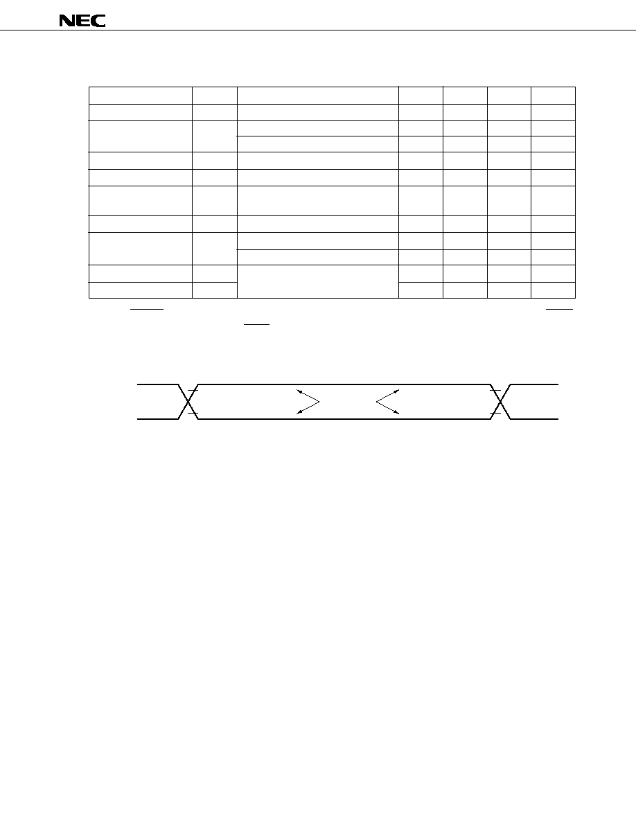
µ
PD78P4038Y
43
DATA RETENTION CHARACTERISTICS (T
A
= ≠40 to +85
∞
C)
Note
RESET, P20/NMI, P21/INTP0, P22/INTP1, P23/INTP2/CI, P24/INTP3, P25/INTP4/ASCK/SCK1,
P26/INTP5, P27/SI0, P32/SCK0/SCL, and P33/SO0/SDA pins
AC TIMING TEST POINTS
Parameter
Data retention voltage
Data retention current
V
DD
rise time
V
DD
fall time
V
DD
hold time
(to STOP mode setting)
STOP clear signal input time
Oscillation settling time
Input low voltage
Input high voltage
Conditions
STOP mode
V
DDDR
= +2.7 to 5.5 V
V
DDDR
= +2.5 V
Crystal
Ceramic resonator
Specific pins
Note
MIN.
2.5
200
200
0
0
30
5
0
0.9V
DDDR
TYP.
30
10
MAX.
5.5
50
40
0.1V
DDDR
V
DDDR
Unit
V
µ
A
µ
A
µ
s
µ
s
ms
ms
ms
ms
V
V
Symbol
V
DDDR
I
DDDR
t
RVD
t
FVD
t
HVD
t
DREL
t
WAIT
V
IL
V
IH
0.8V
DD
or 2.2 V
0.8 V
0.8V
DD
or 2.2 V
0.8 V
Test points
V
DD
- 1 V
0.45 V
µ
PD78P4038Y
44
TIMING WAVEFORM
(1) Read operation
(2) Write operation
ASTB
A8-A19
AD0-AD7
RD
t
WSTH
t
SAST
t
DSTID
t
HSTLA
t
DRST
t
FRA
t
DRID
t
DAR
t
WRL
t
DSTR
t
DAID
t
HRA
t
DRA
t
HRID
ASTB
A8-A19
AD0-AD7
WR
t
WSTH
t
SAST
t
HSTLA
t
DWST
t
DAW
t
DSTW
t
HWOD
t
DSTOD
t
DWOD
t
SODW
t
WWL
t
HWA
µ
PD78P4038Y
45
HOLD TIMING
EXTERNAL WAIT SIGNAL INPUT TIMING
(1) Read operation
(2) Write operation
ASTB
A8-A19
AD0-AD7
RD
WAIT
t
DSTWT
t
HSTWTH
t
DSTWTH
t
DAWT
t
DWTID
t
DWTR
t
DRWTL
t
HRWT
t
DRWTH
ASTB
A8-A19
AD0-AD7
WR
WAIT
t
DSTWT
t
HSTWTH
t
DSTWTH
t
DAWT
t
DWTW
t
DWWTL
t
HWWT
t
DWWTH
HLDRQ
HLDAK
t
DHQHHAH
t
FHQC
t
DCFHA
t
DHAC
t
DHQLHAL
ADTB, A8-A19,
AD0-AD7, RD, WR
µ
PD78P4038Y
46
REFRESH TIMING WAVEFORM
(1) Random read/write cycle
(2) When refresh memory is accessed for a read and write at the same time
(3) Refresh after a read
(4) Refresh after a write
ASTB
WR
RD
t
RC
t
RC
t
RC
t
RC
t
RC
t
WRFQL
ASTB
RD, WR
REFRQ
t
DSTRFQ
t
DRFQST
t
WRFQH
ASTB
RD
REFRQ
t
DRFQST
t
DRRFQ
t
WRFQL
ASTB
WR
REFRQ
t
DRFQST
t
DWRFQ
t
WRFQL
µ
PD78P4038Y
47
SERIAL OPERATION
(1) CSI
(2) I
2
C
(3) IOE1, IOE2
(4) UART, UART2
t
HIGH
t
R
t
HD;DAT
t
SU;DAT
t
F
t
LOW
SCL
SDA
ASCK,
ASCK2
t
WASKH
t
WASKL
t
CYASK
SCK
SI
SO
Output data
Input data
t
SSSK0
t
HSSK0
t
DSBSK1
t
WSKL0
t
WSKH0
t
CYSK0
SCK
SI
SO
Output data
Input data
t
SSSK1
t
HSSK1
t
DSOSK
t
HSOSK
t
WSKL1
t
WSKH1
t
CYSK1
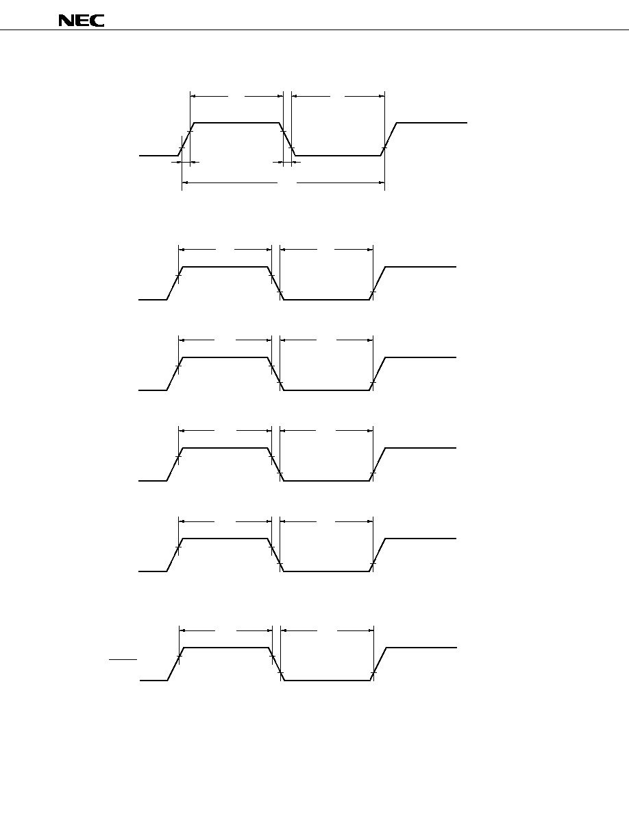
µ
PD78P4038Y
48
CLOCK OUTPUT TIMING
INTERRUPT INPUT TIMING
RESET INPUT TIMING
CLKOUT
t
CLH
t
CLL
t
CYCL
t
CLF
t
CLR
NMI
INTP0
CI,
INTP1-INTP3
INTP4, INTP5
t
WNIH
t
WNIL
t
WIT0H
t
WIT0L
t
WIT1H
t
WIT1L
t
WIT2H
t
WIT2L
RESET
t
WRSH
t
WRSL
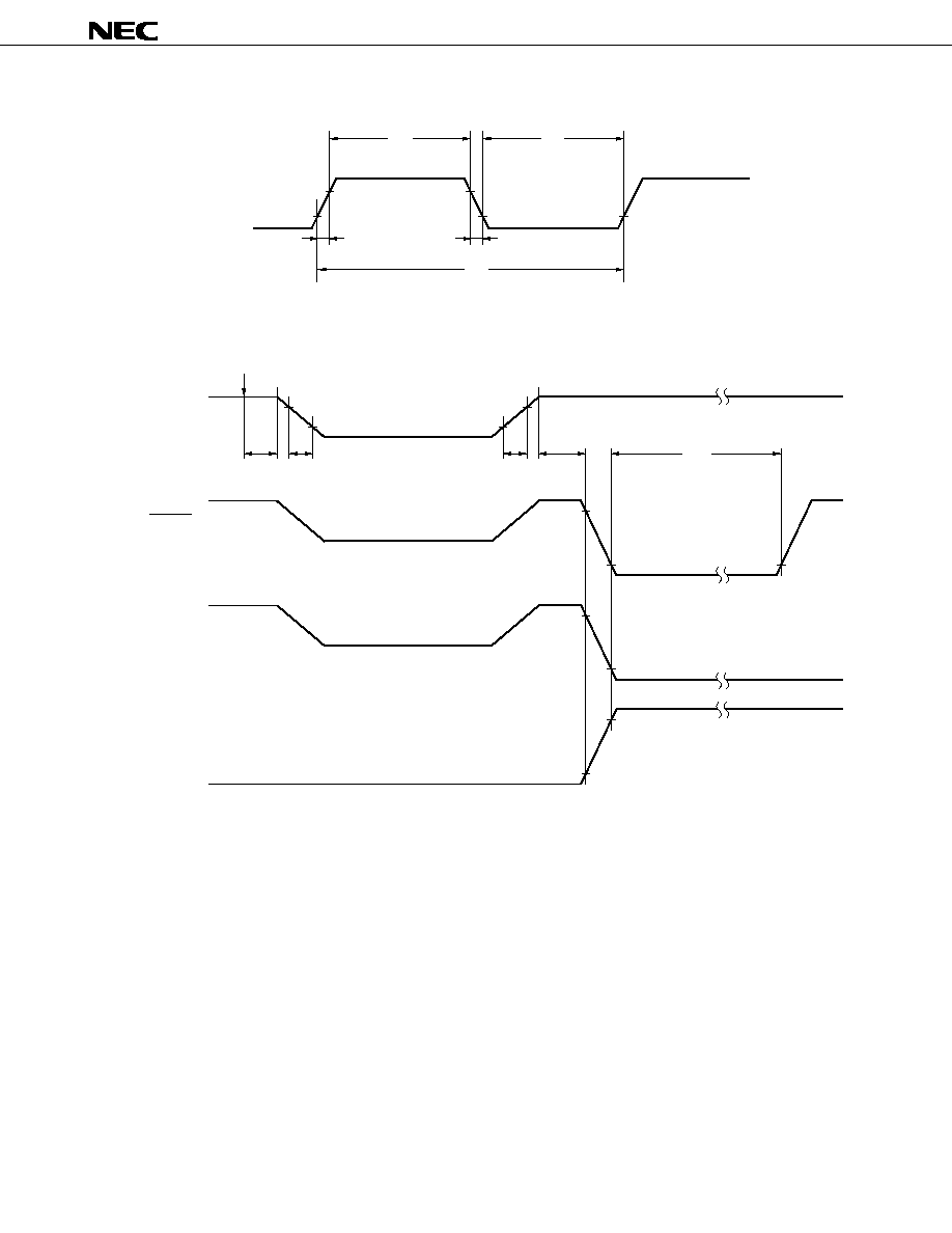
µ
PD78P4038Y
49
EXTERNAL CLOCK TIMING
DATA RETENTION CHARACTERISTICS
X1
t
WXH
t
WXL
t
CYX
t
XF
t
XR
V
DD
RESET
NMI
(Clearing by falling edge)
NMI
(Clearing by rising edge)
t
HVD
t
FVD
t
RVD
t
DREL
V
DDDR
STOP mode setting
t
WAIT
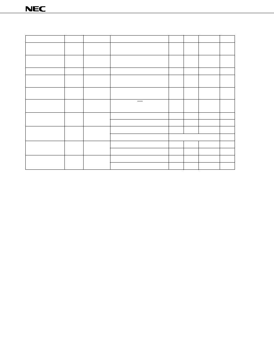
µ
PD78P4038Y
50
Parameter
High-level input
voltage
Low-level input
voltage
Input leakage current
High-level output
voltage
Low-level output
voltage
Output leakage
current
V
DDP
supply voltage
V
PP
supply voltage
V
DDP
supply current
V
PP
supply current
Symbol
V
IH
V
IL
I
LIP
V
OH
V
OL
I
LO
V
DDP
V
PP
I
DD
I
PP
Symbol
Note 1
V
IH
V
IL
I
LI
V
OH
V
OL
≠
V
CC
V
PP
I
DD
I
PP
DC PROGRAMMING CHARACTERISTICS (T
A
= 25
±
5
∞
C, V
SS
= 0 V)
MIN.
2.2
-0.3
2.4
6.25
4.5
12.2
TYP.
6.5
5.0
12.5
10
10
5
1.0
MAX.
V
DDP
+ 0.3
0.8
±
10
0.45
±
10
6.75
5.5
12.8
40
40
50
100
Unit
V
V
µ
A
V
V
µ
A
V
V
V
V
mA
mA
mA
µ
A
Conditions
0
V
I
V
DDP
Note 2
I
OH
= ≠400
µ
A
I
OL
= 2.1 mA
0
V
O
V
DDP
, OE = V
IH
Program memory write mode
Program memory read mode
Program memory write mode
Program memory read mode
Program memory write mode
Program memory read mode
Program memory write mode
Program memory read mode
V
PP
= V
DDP
Notes 1. Symbols for the corresponding
µ
PD27C1001A
2. The V
DDP
represents the V
DD
pin as viewed in the programming mode.
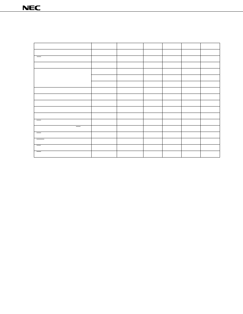
µ
PD78P4038Y
51
Notes 1. These symbols (except t
VDS
) correspond to those of the corresponding
µ
PD27C1001A.
2. For
µ
PD27C1001A, read t
VDS
as t
VCS
.
AC PROGRAMMING CHARACTERISTICS (T
A
= 25
±
5
∞
C, V
SS
= 0 V)
PROM Write Mode (Page Program Mode)
Parameter
Address setup time
CE set time
Input data setup time
Address hold time
Input data hold time
Output data hold time
V
PP
setup time
V
DDP
setup time
Initial program pulse width
OE set time
Valid data delay time from OE
OE pulse width in the data latch
PGM setup time
CE hold time
OE hold time
Symbol
Note 1
t
AS
t
CES
t
DS
t
AH
t
AHL
t
AHV
t
DH
t
DF
t
VPS
t
VDS
Note 2
t
PW
t
OES
t
OE
t
LW
t
PGMS
t
CEH
t
OEH
MIN.
2
2
2
2
2
0
2
0
2
2
0.095
2
1
2
2
2
TYP.
0.1
1
MAX.
130
0.105
2
Unit
µ
s
µ
s
µ
s
µ
s
µ
s
µ
s
µ
s
ns
µ
s
µ
s
ms
µ
s
ns
µ
s
µ
s
µ
s
µ
s
Conditions

µ
PD78P4038Y
52
Notes 1. These symbols (except t
VDS
) correspond to those of the corresponding
µ
PD27C1001A.
2. For
µ
PD27C1001A, read t
VDS
as t
VCS
.
PROM Read Mode
Notes 1. These symbols correspond to those of the corresponding
µ
PD27C1001A.
2. t
DF
is the time measured from when either OE or CE reaches V
IH
, whichever is faster.
PROM Write Mode (Byte Program Mode)
Parameter
Address setup time
CE set time
Input data setup time
Address hold time
Input data hold time
Output data hold time
V
PP
setup time
V
DDP
setup time
Initial program pulse width
OE set time
Valid data delay time from OE
Symbol
Note 1
t
AS
t
CES
t
DS
t
AH
t
DH
t
DF
t
VPS
t
VDS
Note 2
t
PW
t
OES
t
OE
Symbol
Note 1
t
ACC
t
CE
t
OE
t
DF
t
OH
Unit
µ
s
µ
s
µ
s
µ
s
µ
s
ns
µ
s
µ
s
ms
µ
s
ns
Conditions
MAX.
130
0.105
2
TYP.
0.1
1
MIN.
2
2
2
2
2
0
2
2
0.095
2
TYP.
1
1
MIN.
0
0
CE = OE = V
IL
OE = V
IL
CE = V
IL
CE = V
IL
or OE = V
IL
CE = OE = V
IL
Conditions
Parameter
Data output time from address
Delay from CE
to data output
Delay from OE
to data output
Data hold time to OE
or CE
Note 2
Data hold time to address
Unit
ns
µ
s
µ
s
ns
ns
MAX.
200
2
2
60

µ
PD78P4038Y
53
PROM Write Mode Timing (Page Program Mode)
Page data latch
Page program
Program verify
Data
output
Hi-Z
Hi-Z
Hi-Z
A2-A16
A0, A1
D0-D7
V
PP
V
DDP
V
PP
V
DDP
+ 1.5
V
DDP
V
DDP
CE
PGM
OE
V
IH
V
IL
V
IH
V
IL
V
IH
V
IL
t
AS
t
AHL
t
DS
t
DH
t
VPS
Data input
t
PGMS
t
OE
t
VDS
t
AHV
t
DF
t
AH
t
OEH
t
CES
t
CEH
t
PW
t
OES
t
LW
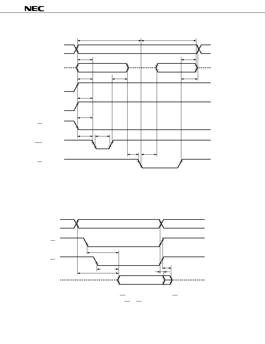
µ
PD78P4038Y
54
PROM Write Mode Timing (Byte Program Mode)
Cautions 1. V
DDP
must be applied before V
PP
, and must be cut after V
PP
.
2. V
PP
including overshoot must not exceed +13.5 V.
3. Plugging in or out the board with the V
PP
pin supplied with 12.5 V may adversely affect its
reliability.
PROM Read Mode Timing
Notes 1. For reading within t
ACC
, the delay of the OE input from falling edge of CE must be within t
ACC
-t
OE
.
2. t
DF
is the time measured from when either OE or CE reaches V
IH
, whichever is faster.
Program
Program verify
A0-A16
V
PP
V
DDP
V
PP
V
DDP
+ 1.5
V
DDP
V
DDP
CE
PGM
V
IH
V
IL
V
IH
V
IL
t
DS
t
PW
Hi-Z
Hi-Z
Hi-Z
D0-D7
V
IH
V
IL
t
AS
t
DS
t
VPS
t
VDS
t
CES
t
DF
t
AH
t
DH
t
OES
t
OE
Data input
Data output
OE
A0-A16
CE
OE
Hi-Z
Hi-Z
D0-D7
Data output
t
CE
Valid address
t
ACC
Note 1
t
OH
t
OE
Note 1
t
DF
Note 2
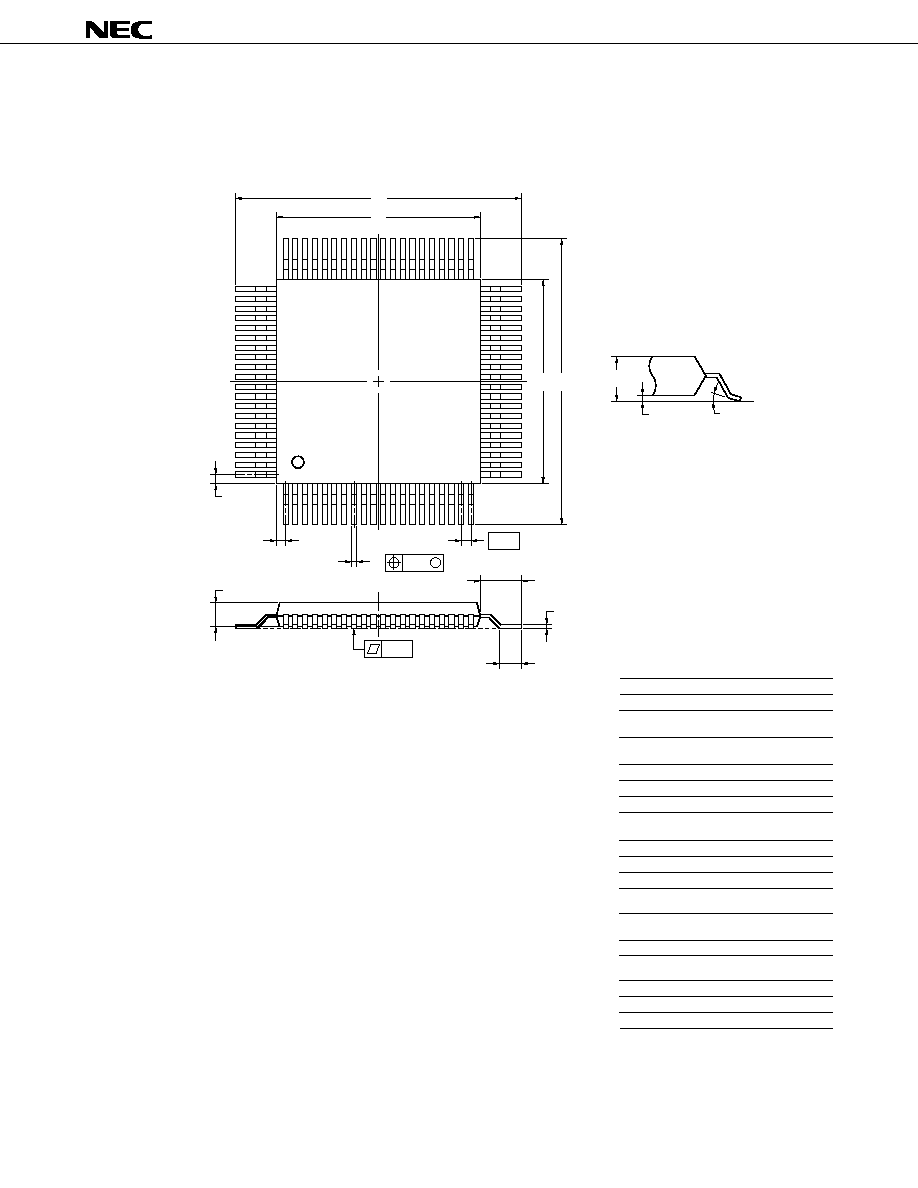
µ
PD78P4038Y
55
12. PACKAGE DRAWINGS
80 PIN PLASTIC QFP (14x14)
ITEM
MILLIMETERS
INCHES
NOTE
Each lead centerline is located within 0.13 mm (0.005 inch) of
its true position (T.P.) at maximum material condition.
L
0.8
±
0.2
0.031+0.009
≠0.008
M
0.15
0.006
N
0.10
0.004
A
17.2
±
0.4
0.677
±
0.016
B
14.0
±
0.2
0.551+0.009
≠0.008
C
14.0
±
0.2
0.551+0.009
≠0.008
D
17.2
±
0.4
0.677
±
0.016
F
0.825
0.032
G
0.825
0.032
H
0.30
±
0.10
0.012+0.004
≠0.005
I
0.13
0.005
J
0.65 (T.P.)
0.026 (T.P.)
Q
0.1
±
0.1
0.004
±
0.004
R
5
∞±
5
∞
5
∞±
5
∞
+0.10
≠0.05
+0.004
≠0.003
M
M
L
K
J
H
Q
P
N
R
detail of lead end
I
G
K
1.6
±
0.2
0.063
±
0.008
60
61
40
80
1
21
20
41
A
B
C D
F
S
S80GC-65-3B9-5
S
3.0 MAX.
0.119 MAX.
P
2.7
±
0.1
0.106+0.005
≠0.004
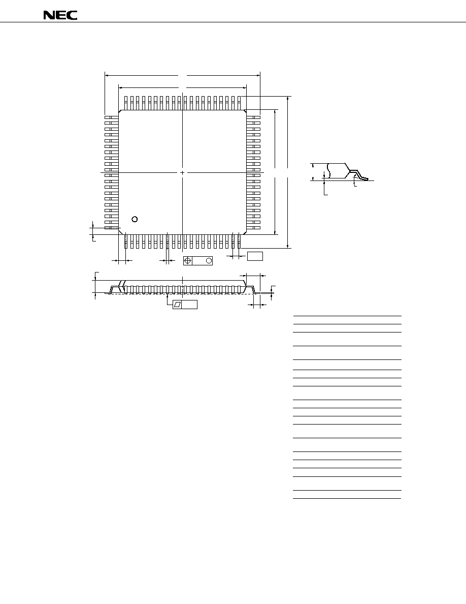
µ
PD78P4038Y
56
80 PIN PLASTIC QFP (14
◊
14)
ITEM
MILLIMETERS
INCHES
NOTE
Each lead centerline is located within 0.13 mm (0.005 inch) of
its true position (T.P.) at maximum material condition.
P80GC-65-8BT
F
0.825
0.032
B
14.00
±
0.20
0.551+0.009
≠0.008
S
1.70 MAX.
0.067 MAX.
M
0.17
0.007+0.001
≠0.003
+0.03
≠0.07
+0.009
≠0.008
C
14.00
±
0.20
0.551+0.009
≠0.008
A
17.20
±
0.20
0.677
±
0.008
G
0.825
0.032
H
0.32
±
0.06
0.013+0.002
≠0.003
I
0.13
0.005
J
0.65 (T.P.)
0.026 (T.P.)
K
1.60
±
0.20
0.063
±
0.008
L
0.80
±
0.20
0.031+0.009
≠0.008
N
0.10
0.004
P
1.40
±
0.10
0.055
±
0.004
Q
0.125
±
0.075
0.005
±
0.003
R
3
∞
3
∞
+7
∞
≠3
∞
+7
∞
≠3
∞
D
17.20
±
0.20
0.677
±
0.008
41
60
40
61
21
80
20
1
M
S
Q
R
K
M
L
A
B
C
D
J
H
I
F
G
P
N
detail of lead end

µ
PD78P4038Y
57
80 PIN PLASTIC TQFP (FINE PITCH) (12
◊
12)
ITEM
MILLIMETERS
INCHES
I
J
0.50 (T.P.)
0.10
0.004
0.020 (T.P.)
NOTE
Each lead centerline is located within 0.10 mm (0.004 inch) of
its true position (T.P.) at maximum material condition.
A
14.00
±
0.20
0.551
±
0.008
B
12.00
±
0.20
0.472+0.009
≠0.008
C
12.00
±
0.20
0.472+0.009
≠0.008
D
14.00
±
0.20
0.551
±
0.008
F
G
1.25
1.25
0.049
0.049
H
0.22
0.009
±
0.002
P80GK-50-BE9-5
S
1.27 MAX.
0.050 MAX.
K
1.00
±
0.20
0.039+0.009
≠0.008
L
0.50
±
0.20
0.020+0.008
≠0.009
M
0.145
0.006
±
0.002
N
0.10
0.004
P
1.05
0.041
Q
0.10
±
0.05
0.004
±
0.002
R
5
∞±
5
∞
5
∞±
5
∞
+0.05
≠0.04
+0.055
≠0.045
J
N
L
K
M
detail of lead end
61
60
41
40
21
20
1
80
A
B
C
D
S
Q
R
G
F
P
H
I
M
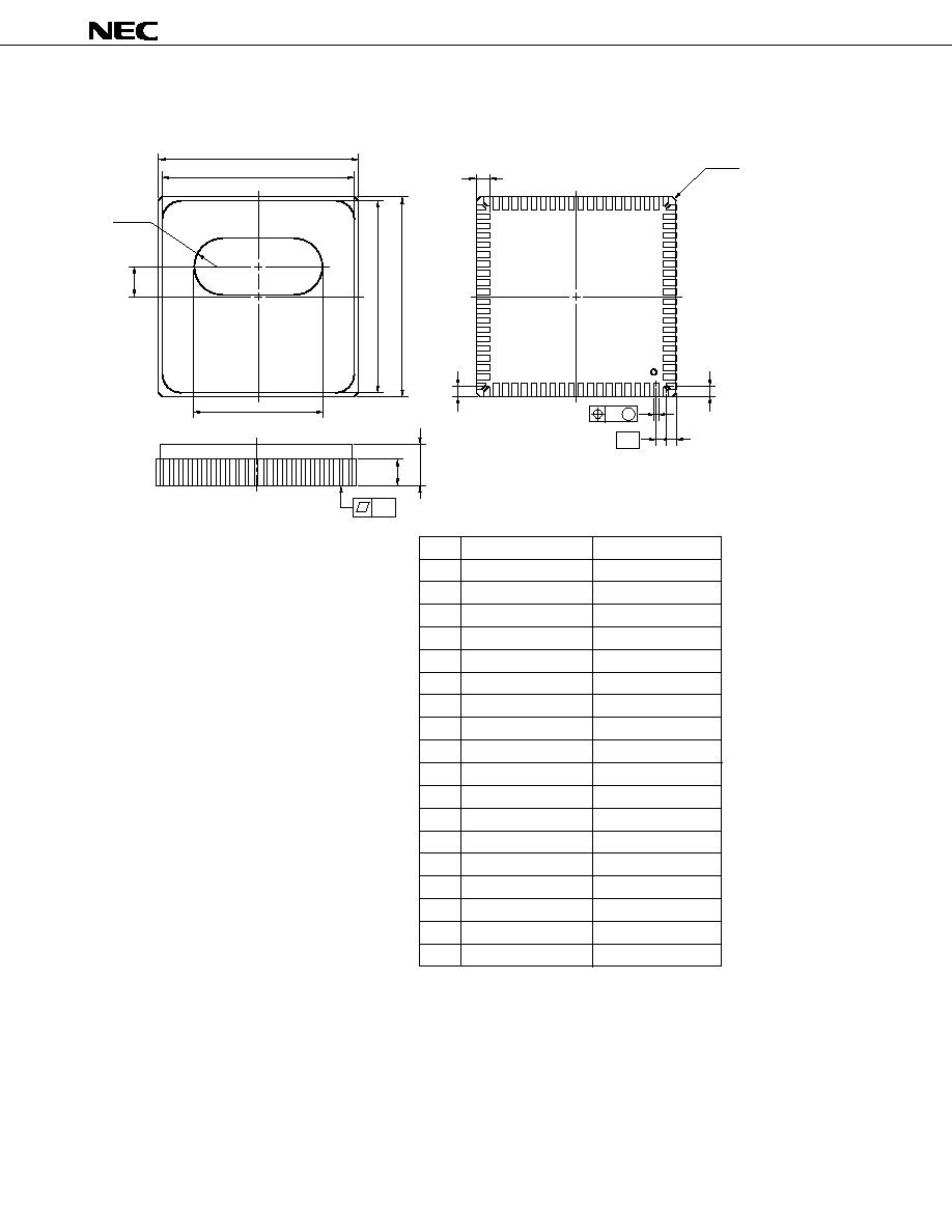
µ
PD78P4038Y
58
Z
U1
A
T
B
D
C
U
G
F
W
R
S
Q
K
M
I
H
J
X80KW-65A-1
ITEM
MILLIMETERS
INCHES
A
B
C
D
F
G
H
I
J
K
Q
14.0
±
0.2
13.6
3.6 MAX.
0.06
13.6
0.551
±
0.008
0.072
0.142 MAX.
0.003
0.024 (T.P.)
0.535
NOTE
R
S
0.825
0.825
0.65 (T.P.)
0.032
0.032
Each lead centerline is located within 0.06
mm (0.003 inch) of its true position (T.P.) at
maximum material condition.
0.018
0.535
T
R 2.0
R 0.079
0.551
±
0.008
14.0
±
0.2
1.84
U
9.0
0.354
U1
2.1
0.083
+0.004
≠0.005
W
Z
0.10
0.004
80
1
0.45
±
0.10
0.039
+0.007
≠0.006
1.0
±
0.15
C 0.3
C 0.012
0.75
±
0.15
0.030
+0.006
≠0.007
80 PIN CERAMIC WQFN
µ
PD78P4038Y
59
13. RECOMMENDED SOLDERING CONDITIONS
The conditions listed below shall be met when soldering the
µ
PD78P4038Y.
For details of the recommended soldering conditions, refer to our document Semiconductor Device Mounting
Technology Manual (C10535E).
Please consult with our sales offices in case any other soldering process is used, or in case soldering is done under
different conditions.
Table 13-1. Soldering Conditions for Surface-Mount Devices (1/2)
(1)
µ
PD78P4038YGC-3B9: 80-pin plastic QFP (14
◊
14
◊
2.7 mm)
Caution Do not apply two or more different soldering methods to one chip (except for partial heating
method for terminal sections).
(2)
µ
PD78P4038YGC-8BT: 80-pin plastic QFP (14
◊
14
◊
1.4 mm)
Caution Do not apply two or more different soldering methods to one chip (except for partial heating
method for terminal sections).
Soldering Process
Soldering Conditions
Symbol
Infrared ray reflow
Peak package's surface temperature: 235
∞
C
IR35-00-2
Reflow time: 30 seconds or less (210
∞
C or more)
Maximum allowable number of reflow processes: 2
VPS
Peak package's surface temperature: 215
∞
C
VP15-00-2
Reflow time: 40 seconds or less (200
∞
C or more)
Maximum allowable number of reflow processes: 2
Wave soldering
Solder temperature: 260
∞
C or less
WS60-00-1
Flow time: 10 seconds or less
Number of flow processes: 1
Preheating temperature
: 120
∞
C max. (measured on the package surface)
Partial heating method
Terminal temperature: 300
∞
C or less
≠
Heat time: 3 seconds or less (for one side of a device)
Soldering Process
Soldering Conditions
Symbol
Infrared ray reflow
Peak package's surface temperature: 235
∞
C
IR35-00-3
Reflow time: 30 seconds or less (210
∞
C or more)
Maximum allowable number of reflow processes: 3
VPS
Peak package's surface temperature: 215
∞
C
VP15-00-3
Reflow time: 40 seconds or less (200
∞
C or more)
Maximum allowable number of reflow processes: 3
Wave soldering
Solder temperature: 260
∞
C or less
WS60-00-1
Flow time: 10 seconds or less
Number of flow processes: 1
Preheating temperature
: 120
∞
C max. (measured on the package surface)
Partial heating method
Terminal temperature: 300
∞
C or less
≠
Heat time: 3 seconds or less (for one side of a device)

µ
PD78P4038Y
60
Table 13-1. Soldering Conditions for Surface-Mount Devices (2/2)
(3)
µ
PD78P4038YGK-BE9: 80-pin plastic TQFP (fine pitch) (12
◊
12 mm)
Note
Maximum number of days during which the product can be stored at a temperature of 25
∞
C and a relative
humidity of 65% or less after dry-pack package is opened.
Caution Do not apply two or more different soldering methods to one chip (except for partial heating
method for terminal sections).
Soldering Process
Infrared ray reflow
VPS
Partial heating method
Symbol
IR35-107-2
VP15-107-2
≠
Soldering Conditions
Peak package's surface temperature: 235
∞
C
Reflow time: 30 seconds or less (210
∞
C or more)
Maximum allowable number of reflow processes: 2
Exposure limit: 7 days
Note
(10 hours of pre-baking is required at 125
∞
C
afterward)
<Caution>
Non-heat-resistant trays, such as magazine and taping trays, cannot be
baked before unpacking.
Peak package's surface temperature: 215
∞
C
Reflow time: 40 seconds or less (200
∞
C or more)
Maximum allowable number of reflow processes: 2
Exposure limit: 7 days
Note
(10 hours of pre-baking is required at 125
∞
C
afterward)
<Caution>
Non-heat-resistant trays, such as magazine and taping trays, cannot be
baked before unpacking.
Terminal temperature: 300
∞
C or less
Heat time: 3 seconds or less (for one side of a device)

µ
PD78P4038Y
61
APPENDIX A DEVELOPMENT TOOLS
The following development tools are available for system development using the
µ
PD78P4038Y.
See also (5).
(1) Language processing software
RA78K4
Assembler package for all 78K/IV Series models
CC78K4
C compiler package for all 78K/IV Series models
DF784038
Device file for
µ
PD784038Y Subseries models
CC78K4-L
C compiler library source file for all 78K/IV Series models
(2) PROM write tools
PG-1500
PROM programmer
PA-78P4026GC
Programmer adaptor, connects to PG-1500
PA-78P4038GK
PA-78P4026KK
PG-1500 controller
Control program for PG-1500
(3) Debugging tools
∑ When using the in-circuit emulator IE-78K4-NS
IE-78K4-NS
In-circuit emulator for all 78K/IV Series models
IE-70000-MC-PS-B
Power supply unit for IE-78K4-NS
IE-70000-98-IF-C
Interface adapter when the PC-9800 series computer (other than a notebook)
is used as the host machine
IE-70000-CD-IF
PC card and interface cable when a PC-9800 series notebook is used as the
host machine
IE-70000-PC-IF-C
Interface adapter when the IBM PC/AT
TM
or compatible is used as the host
machine
IE-784038-NS-EM1
Note
Emulation board for evaluating
µ
PD784038Y Subseries models
NP-80GC
Emulation probe for 80-pin plastic QFP (GC-3B9 and GC-8BT types)
NP-80GK
Note
Emulation probe for 80-pin plastic TQFP (GK-BE9 type)
EV-9200GC-80
Socket for mounting on target system board made for 80-pin plastic QFP
(GC-3B9 and GC-8BT types)
TGK-080SDW
Adapter for mounting on target system board made for 80-pin plastic TQFP
(fine pitch) (GK-BE9 type)
EV-9900
Tool used to remove the
µ
PD78P4038YKK-T from the EV-9200GC-80
ID78K4-NS
Integrated debugger for IE-78K4-NS
SM78K4-NS
System simulator for all 78K/IV Series models
DF784038
Device file for
µ
PD784038Y Subseries models
Note
Under development
µ
PD78P4038Y
62
∑ When using the in-circuit emulator IE-784000-R
IE-784000-R
In-circuit emulator for all 78K/IV Series models
IE-70000-98-IF-B
Interface adapter when the PC-9800 series computer (other than a notebook)
IE-70000-98-IF-C
is used as the host machine
IE-70000-98N-IF
Interface adapter and cable when a PC-9800 series notebook is used as the
host machine
IE-70000-PC-IF-B
Interface adapter when the IBM PC/AT or compatible is used as the host
IE-70000-PC-IF-C
machine
IE-78000-R-SV3
Interface adapter and cable when the EWS is used as the host machine
IE-784038-NS-EM1
Note
Emulation board for evaluating
µ
PD784038Y Subseries models
IE-784038-R-EM1
IE-78400-R-EM
Emulation board for all 78K/IV Series models
IE-78K4-R-EX2
Note
Conversion board for 80 pins to use the IE-784038-NS-EM1 on the
IE-784000-R. The board is not needed when the conventional product
IE-784038-R-EM1 is used.
EP-78230GC-R
Emulation probe for 80-pin plastic QFP (GC-3B9 and GC-8BT types)
EP-78054GK-R
Emulation probe for 80-pin plastic TQFP (fine pitch) (GK-BE9 type) for all
µ
PD784038Y Subseries
EV-9200GC-80
Socket for mounting on target system board made for 80-pin plastic QFP
(GC-3B9 and GC-8BT types)
TGK-080SDW
Adapter for mounting on target system board made for 80-pin plastic TQFP
(fine pitch) (GK-BE9 type)
EV-9900
Tool used to remove the
µ
PD78P4038YKK-T from the EV-9200GC-80
ID78K4
Integrated debugger for IE-784000-R
SM78K4
System simulator for all 78K/IV Series models
DF784038
Device file for
µ
PD784038Y Subseries models
Note Under development
(4) Real-time OS
RX78K/IV
Real-time OS for 78K/IV Series models
MX78K4
OS for 78K/IV Series models
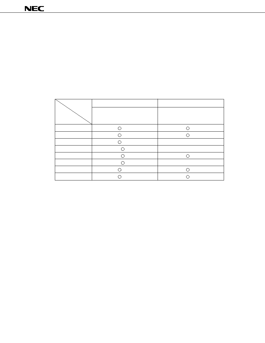
µ
PD78P4038Y
63
(5) Notes when using development tools
∑ The ID78K-NS, ID78K4, and SM78K4 can be used in combination with the DF784038.
∑ The CC78K4 and RX78K/IV can be used in combination with the RA78K4 and DF784038.
∑ The NP-80GC is a product from Naito Densei Machida Mfg. Co., Ltd. (044-822-3813). Consult the NEC sales
representative for purchasing.
∑ The TGK-080SDW is a product from TOKYO ELETECH CORPORATION.
Refer to: Daimaru Kogyo, Ltd.
Tokyo Electronic Components Division (03-3820-7112)
Osaka Electronic Components Division (06-244-6672)
∑ The host machines and operating systems corresponding to each software are shown below.
Host Machine
PC
EWS
[OS]
PC-9800 Series [Windows
TM
]
HP9000 Series 700
TM
[HP-UX
TM
]
IBM PC/AT and Compatibles [Windows] SPARCstation
TM
[SunOS
TM
]
Software
NEWS
TM
(RISC) [NEWS-OS
TM
]
RA78K4
Note
CC78K4
Note
PG-1500 controller
Note
≠
ID78K4-NS
≠
ID78K4
SM78K4
≠
RX78K/IV
Note
MX78K4
Note
Note Software under MS-DOS
µ
PD78P4038Y
64
APPENDIX B CONVERSION SOCKET (EV-9200GC-80) AND CONVERSION ADAPTER (TGK-080SDW)
(1) Conversion socket (EV-9200GC-80) package drawings and recommended pattern to mount the socket
Connect the
µ
PD78P4038YKK-T (80-pin ceramic WQFN (14
◊
14 mm)) and EP-78230GC-R to the circuit board
in combination with the EV-9200GC-80.
Figure B-1. Package Drawings of EV-9200GC-80 (Reference) (unit: mm)
A
F
D
1
No.1 pin index
E
EV-9200GC-80
B
C
M
N
O
L
K
S
R
Q
P
I
H
J
G
EV-9200GC-80-G0E
ITEM
MILLIMETERS
INCHES
A
B
C
D
E
F
G
H
I
J
K
L
M
O
N
P
Q
R
S
18.0
14.4
14.4
18.0
4-C 2.0
0.8
6.0
16.0
18.7
6.0
16.0
18.7
8.2
8.0
2.5
2.0
0.35
2.3
1.5
0.709
0.567
0.567
0.709
4-C 0.079
0.031
0.236
0.63
0.736
0.236
0.63
0.736
0.323
0.315
0.098
0.079
0.014
0.091
0.059
Based on EV-9200GC-80
(1) Package drawing (in mm)
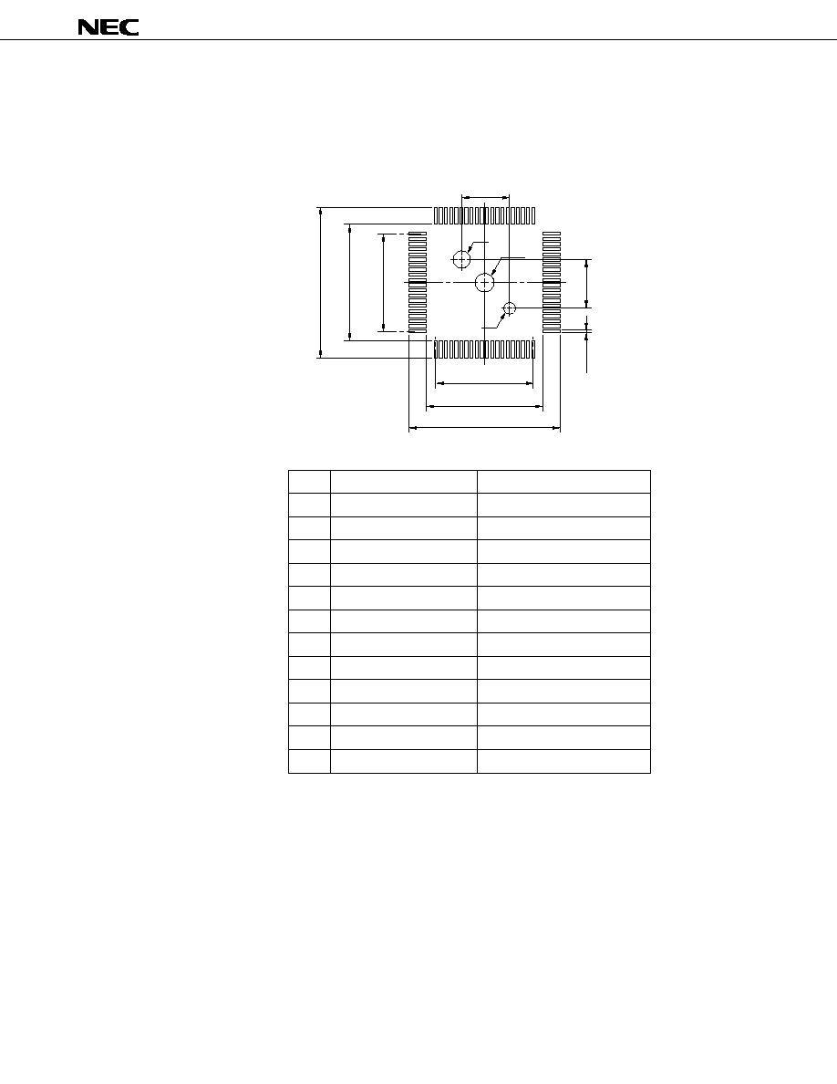
µ
PD78P4038Y
65
Figure B-2. Recommended Pattern to Mount EV-9200GC-80 on a Substrate (Reference) (unit: mm)
A
F
D
E
C
B
G
J
K
L
H
I
0.026
◊
0.748=0.486
0.026
0.748=0.486
EV-9200GC-80-P1E
ITEM
MILLIMETERS
INCHES
A
B
C
D
E
F
G
H
I
J
K
L
19.7
15.0
15.0
19.7
6.0
±
0.05
6.0
±
0.05
0.35
±
0.02
2.36
±
0.03
2.3
1.57
±
0.03
0.776
0.591
0.591
0.776
0.236
0.236
0.014
0.093
0.091
0.062
0.65
±
0.02
◊
19=12.35
±
0.05
0.65
±
0.02
◊
19=12.35
±
0.05
+0.001
≠0.002
+0.003
≠0.002
+0.001
≠0.002
+0.003
≠0.002
+0.003
≠0.002
+0.003
≠0.002
+0.001
≠0.001
+0.001
≠0.002
+0.001
≠0.002
Based on EV-9200GC-80
(2) Pad drawing (in mm)
Dimensions of mount pad for EV-9200 and that for target
device (QFP) may be different in some parts. For the
recommended mount pad dimensions for QFP, refer to
"SEMICONDUCTOR DEVICE MOUNTING
TECHNOLOGY MANUAL" (C10535E).
Caution
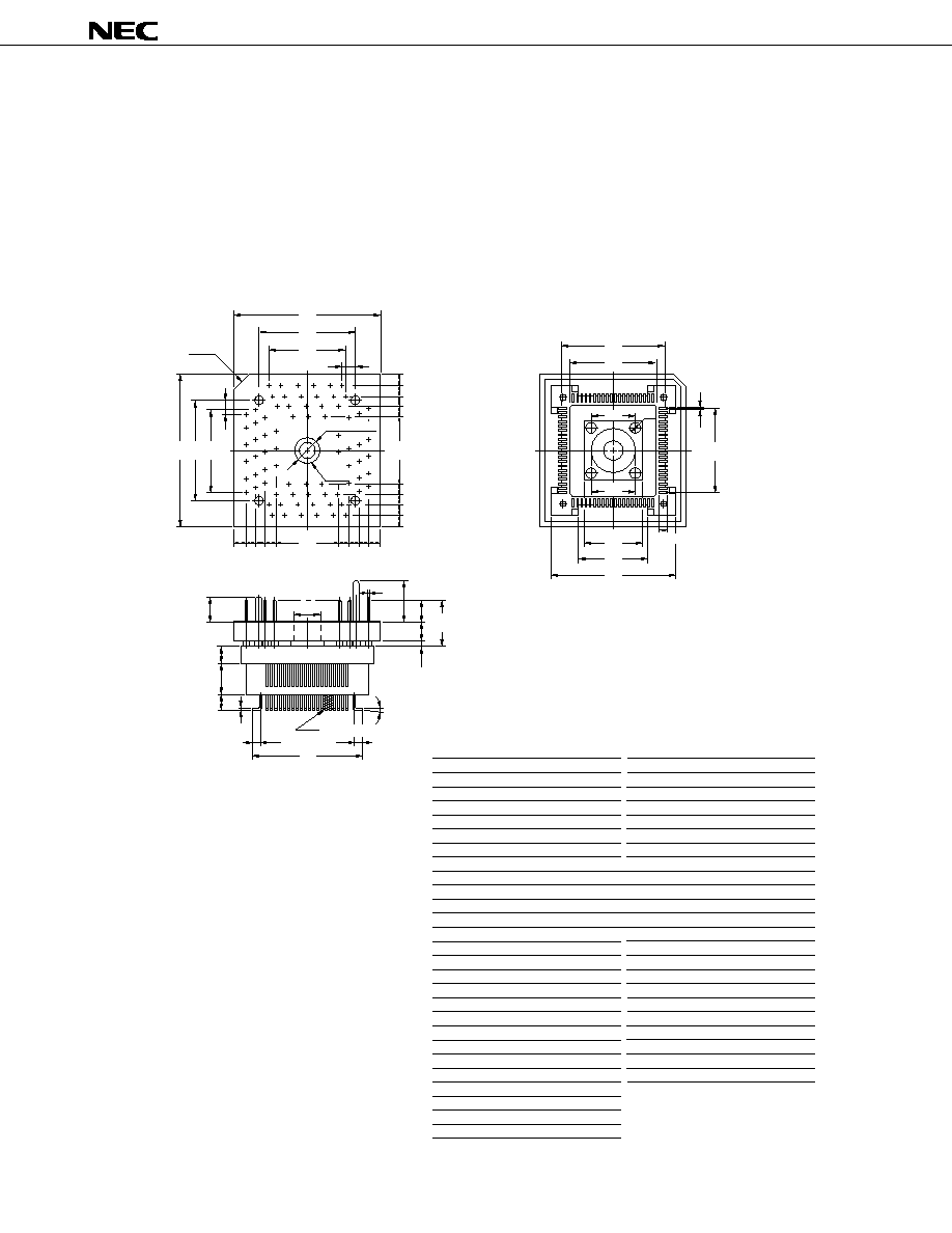
µ
PD78P4038Y
66
(2) Conversion adapter (TGK-080SDW) package drawings
Connect the EP-78054GK-R to the circuit board in combination with the TGK-080SDW.
Figure B-3. Package Drawings of TGK-080SDW (Reference) (unit: mm)
ITEM
MILLIMETERS
INCHES
b
0.25
0.010
c
5.3
0.209
a
0.5x19=9.5
±
0.10
0.020x0.748=0.374
±
0.004
d
5.3
0.209
h
1.85
±
0.2
0.073
±
0.008
i
3.5
0.138
j
2.0
0.079
e
1.3
0.051
f
3.55
g
0.3
0.012
0.140
ITEM
MILLIMETERS
INCHES
B
C
0.5x19=9.5
0.020x0.748=0.374
A
18.0
0.709
D
H
I
1.58
0.062
J
1.2
0.047
E
0.5x19=9.5
0.020x0.748=0.374
F
11.77
0.463
K
7.64
0.301
L
1.2
0.047
M
Q
1.2
0.047
R
1.58
0.062
S
3.55
0.140
N
1.58
0.062
O
1.2
P
7.64
0.301
0.047
W
6.8
0.268
X
8.24
0.324
Y
14.8
0.583
T
C 2.0
C 0.079
U
12.31
V
10.17
0.400
0.485
Z
1.4
±
0.2
0.055
±
0.008
0.5
1.58
0.020
0.062
G
18.0
0.709
k
3.0
0.118
n
1.4
±
0.2
0.055
±
0.008
o
1.4
±
0.2
0.055
±
0.008
p
h=1.8 1.3
h=0.071 0.051
l
0.25
m
14.0
0.551
0.010
q
0~5
∞
0.000~0.197
∞
11.77
0.5
0.463
0.020
TGK-080SDW-G1E
t
2.4
0.094
u
2.7
0.106
v
3.9
0.154
r
5.9
s
0.8
0.031
0.232
TGK-080SDW (TQPACK080SD + TQSOCKET080SDW)
Package dimension (unit: mm)
E
F
G
P
R
Q
Q
Q
O
O
O
N
I J J J
L L LM
B
C
A
T
H
D
K
S
M2 screw
U
a
V
e
c
d
b
W
X
Y
Z
m
f
r
u
t
v
g
s
k
j
i
h
l
n
o
p
Protrusion : 4 places
q
note: Product by TOKYO ELETECH CORPORATION.
µ
PD78P4038Y
67
APPENDIX C RELATED DOCUMENTS
Documents Related to Devices
Document Name
Document No.
English
Japanese
µ
PD784031Y Data Sheet
U11504E
U11504J
µ
PD784035Y, 784036Y, 784037Y, 784038Y Data Sheet
U10741E
U10741J
µ
PD78P4038Y Data Sheet
This manual
U10742J
µ
PD784038, 784038Y Sub-Series User's Manual, Hardware
U11316E
U11316J
µ
PD784038Y Sub-Series Special Function Registers
≠
U11090J
78K/IV Series User's Manual, Instruction
U10905E
U10905J
78K/IV Series Instruction Summary Sheet
≠
U10594J
78K/IV Series Instruction Set
≠
U10595J
78K/IV Series Application Note, Software Basic
≠
U10095J
Documents Related to Development Tools (User's Manual)
Document Name
Document No.
English
Japanese
RA78K4 Assembler Package
Operation
U11334E
U11334J
Language
U11162E
U11162J
RA78K Series Structured Assembler Preprocessor
U11743E
U11743J
CC78K4 Series
Operation
U11572E
U11572J
Language
U11571E
U11571J
CC78K Series Library Source File
U12322E
U12322J
PG-1500 PROM Programmer
U11940E
U11940J
PG-1500 Controller PC-9800 Series (MS-DOS
TM
) Base
EEU-1291
EEU-704
PG-1500 Controller IBM PC Series (PC DOS
TM
) Base
U10540E
EEU-5008
IE-78K4-NS
To be released
U13356J
soon
IE-784000-R
EEU-1534
U12903J
IE-784038-NS-EM1
Planned
Planned
IE-784038-R-EM1
U11383E
U11383J
EP-78230
EEU-1515
EEU-985
EP-78054GK-R
EEU-1468
EEU-932
SM78K4 System Simulator Windows Base
Reference
U10093E
U10093J
SM78K Series System Simulator
External Parts User Open
U10092E
U10092J
Interface Specifications
ID78K4-NS Integrated Debugger
Reference
U12796E
U12796J
ID78K4 Integrated Debugger Windows Base
Reference
U10440E
U10440J
ID78K4 Integrated Debugger HP-UX, SunOS, NEWS-OS Base
Reference
U11960E
U11960J
Caution The above documents may be revised without notice. Use the latest versions when you design
application systems.
µ
PD78P4038Y
68
Documents Related to Software to Be Incorporated into the Product (User's Manual)
Document Name
Document No.
English
Japanese
78K/IV Series Real-Time OS
Basic
U10603E
U10603J
Installation
U10604E
U10604J
Debugger
≠
U10364J
OS for 78K/IV Series MX78K4
Basic
≠
U11779J
Other Documents
Document Name
Document No.
English
Japanese
IC PACKAGE MANUAL
C10943X
Semiconductor Device Mounting Technology Manual
C10535E
C10535J
Quality Grades on NEC Semiconductor Device
C11531E
C11531J
NEC Semiconductor Device Reliability/Quality Control System
C10983E
C10983J
Guide to Prevent Damage for Semiconductor Devices by Electrostatic Discharge (ESD)
C11892E
C11892J
Semiconductor Device Quality Control/Reliability Handbook
≠
C12769J
Guide for Products Related to Microcomputer: Other Companies
≠
U11416J
Caution The above documents may be revised without notice. Use the latest versions when you design
application systems.
µ
PD78P4038Y
69
NOTES FOR CMOS DEVICES
1
PRECAUTION AGAINST ESD FOR SEMICONDUCTORS
Note: Strong electric field, when exposed to a MOS device, can cause destruction of
the gate oxide and ultimately degrade the device operation. Steps must be taken
to stop generation of static electricity as much as possible, and quickly dissipate
it once, when it has occurred. Environmental control must be adequate. When
it is dry, humidifier should be used. It is recommended to avoid using insulators
that easily build static electricity. Semiconductor devices must be stored and
transported in an anti-static container, static shielding bag or conductive
material. All test and measurement tools including work bench and floor should
be grounded. The operator should be grounded using wrist strap. Semiconduc-
tor devices must not be touched with bare hands. Similar precautions need to
be taken for PW boards with semiconductor devices on it.
2
HANDLING OF UNUSED INPUT PINS FOR CMOS
Note: No connection for CMOS device inputs can be cause of malfunction. If no
connection is provided to the input pins, it is possible that an internal input level
may be generated due to noise, etc., hence causing malfunction. CMOS device
behave differently than Bipolar or NMOS devices. Input levels of CMOS devices
must be fixed high or low by using a pull-up or pull-down circuitry. Each unused
pin should be connected to V
DD
or GND with a resistor, if it is considered to have
a possibility of being an output pin. All handling related to the unused pins must
be judged device by device and related specifications governing the devices.
3
STATUS BEFORE INITIALIZATION OF MOS DEVICES
Note: Power-on does not necessarily define initial status of MOS device. Production
process of MOS does not define the initial operation status of the device.
Immediately after the power source is turned ON, the devices with reset function
have not yet been initialized. Hence, power-on does not guarantee out-pin
levels, I/O settings or contents of registers. Device is not initialized until the
reset signal is received. Reset operation must be executed immediately after
power-on for devices having reset function.

µ
PD78P4038Y
70
Caution This product contains an I
2
C bus interface circuit.
When using the I
2
C bus interface, notify its use to NEC when ordering custom code. NEC can
guarantee the following only when the customer informs NEC of the use of the interface:
Purchase of NEC I
2
C components conveys a license under the Philips I
2
C Patent Rights to use
these components in an I
2
C system, provided that the system conforms to the I
2
C Standard
Specification as defined by Philips.
IEBus and QTOP are trademarks of NEC Corporation.
MS-DOS and Windows are registered trademarks or trademarks of Microsoft Corporation in the United States
and/or other countries.
PC/AT and PC DOS are trademarks of IBM Corporation.
HP9000 series 700 and HP-UX are trademarks of Hewlett-Packard Company.
SPARCstation is a trademark of SPARC International, Inc.
SunOS is a trademark of Sun Microsystems, Inc.
NEWS and NEWS-OS are trademarks of SONY Corporation.

µ
PD78P4038Y
71
Regional Information
Some information contained in this document may vary from country to country. Before using any NEC
product in your application, pIease contact the NEC office in your country to obtain a list of authorized
representatives and distributors. They will verify:
∑
Device availability
∑
Ordering information
∑
Product release schedule
∑
Availability of related technical literature
∑
Development environment specifications (for example, specifications for third-party tools and
components, host computers, power plugs, AC supply voltages, and so forth)
∑
Network requirements
In addition, trademarks, registered trademarks, export restrictions, and other legal issues may also vary
from country to country.
NEC Electronics Inc. (U.S.)
Santa Clara, California
Tel: 408-588-6000
800-366-9782
Fax: 408-588-6130
800-729-9288
NEC Electronics (Germany) GmbH
Duesseldorf, Germany
Tel: 0211-65 03 02
Fax: 0211-65 03 490
NEC Electronics (UK) Ltd.
Milton Keynes, UK
Tel: 01908-691-133
Fax: 01908-670-290
NEC Electronics Italiana s.r.1.
Milano, Italy
Tel: 02-66 75 41
Fax: 02-66 75 42 99
NEC Electronics (Germany) GmbH
Benelux Office
Eindhoven, The Netherlands
Tel: 040-2445845
Fax: 040-2444580
NEC Electronics (France) S.A.
Velizy-Villacoublay, France
Tel: 01-30-67 58 00
Fax: 01-30-67 58 99
NEC Electronics (France) S.A.
Spain Office
Madrid, Spain
Tel: 01-504-2787
Fax: 01-504-2860
NEC Electronics (Germany) GmbH
Scandinavia Office
Taeby, Sweden
Tel: 08-63 80 820
Fax: 08-63 80 388
NEC Electronics Hong Kong Ltd.
Hong Kong
Tel: 2886-9318
Fax: 2886-9022/9044
NEC Electronics Hong Kong Ltd.
Seoul Branch
Seoul, Korea
Tel: 02-528-0303
Fax: 02-528-4411
NEC Electronics Singapore Pte. Ltd.
United Square, Singapore 1130
Tel: 65-253-8311
Fax: 65-250-3583
NEC Electronics Taiwan Ltd.
Taipei, Taiwan
Tel: 02-719-2377
Fax: 02-719-5951
NEC do Brasil S.A.
Cumbica-Guarulhos-SP, Brasil
Tel: 011-6465-6810
Fax: 011-6465-6829
J98. 2

µ
PD78P4038Y
Some related documents may be preliminary versions. Note that, however, what documents are preliminary is not indicated
in this document.
License not needed
:
µ
PD78P4038YKK-T
The customer must judge the need for license
:
µ
PD78P4038YGC-3B9,
µ
PD78P4038YGC-
◊◊◊
-3B9,
µ
PD78P4038YGC-8BT
µ
PD78P4038YGK-BE9,
µ
PD78P4038YGK-
◊◊◊
-BE9
The export of these products from Japan is regulated by the Japanese government. The export of some or all of these
products may be prohibited without governmental license. To export or re-export some or all of these products from a
country other than Japan may also be prohibited without a license from that country. Please call an NEC sales
representative.
No part of this document may be copied or reproduced in any form or by any means without the prior written
consent of NEC Corporation. NEC Corporation assumes no responsibility for any errors which may appear in this
document.
NEC Corporation does not assume any liability for infringement of patents, copyrights or other intellectual
property rights of third parties by or arising from use of a device described herein or any other liability arising
from use of such device. No license, either express, implied or otherwise, is granted under any patents,
copyrights or other intellectual property rights of NEC Corporation or others.
While NEC Corporation has been making continuous effort to enhance the reliability of its semiconductor devices,
the possibility of defects cannot be eliminated entirely. To minimize risks of damage or injury to persons or
property arising from a defect in an NEC semiconductor device, customers must incorporate sufficient safety
measures in its design, such as redundancy, fire-containment, and anti-failure features.
NEC devices are classified into the following three quality grades:
"Standard", "Special", and "Specific". The Specific quality grade applies only to devices developed based on
a customer designated "quality assurance program" for a specific application. The recommended applications
of a device depend on its quality grade, as indicated below. Customers must check the quality grade of each
device before using it in a particular application.
Standard: Computers, office equipment, communications equipment, test and measurement equipment,
audio and visual equipment, home electronic appliances, machine tools, personal electronic
equipment and industrial robots
Special: Transportation equipment (automobiles, trains, ships, etc.), traffic control systems, anti-disaster
systems, anti-crime systems, safety equipment and medical equipment (not specifically designed
for life support)
Specific: Aircrafts, aerospace equipment, submersible repeaters, nuclear reactor control systems, life
support systems or medical equipment for life support, etc.
The quality grade of NEC devices is "Standard" unless otherwise specified in NEC's Data Sheets or Data Books.
If customers intend to use NEC devices for applications other than those specified for Standard quality grade,
they should contact an NEC sales representative in advance.
Anti-radioactive design is not implemented in this product.
M4 96. 5