Document Outline
- COVER
- FEATURES
- ORDERING INFORMATION
- 78K/IV Series Products
- Function List
- Pin Configuration (Top View)
- Internal Block Diagram
- System Configuration Example
- 1. DIFFERENCES BETWEEN uPD78P4916 AND uPD784915, uPD784916A
- 2. PIN FUNCTION
- 2.1 Normal Operation Mode
- 2.2 PROM Programming Mode (VPP Greater or equal to 5 V, RESET# = L)
- 2.3 Pin I/O Circuits and Recommended Connection of Unused Pins
- 3. INTERNAL MEMORY CAPACITY SELECT REGISTER (IMS)
- 4. PROM PROGRAMMING
- 4.1 Operation Mode
- 4.2 PROM Write Procedure
- 4.3 PROM Read Procedure
- 4.4 Screening One-time PROM Versions
- 5. ELECTRICAL SPECIFICATIONS
- 6. PACKAGE DRAWING
- 7. RECOMMENDED SOLDERING CONDITIONS
- APPENDIX A. DEVELOPMENT TOOLS
- APPENDIX B. SOCKET DRAWING AND RECOMMENDED FOOTPRINT
- APPENDIX C. RELATED DOCUMENTS

©
1996
DATA SHEET
The
µ
PD78P4916 is one of the
µ
PD784915 subseries in the 78K/IV Series microcontrollers which incorporate
a high-speed and high-performance 16-bit CPU.
The
µ
PD78P4916 replaces mask ROM with one-time PROM and increases on-chip ROM and RAM capacity
compared to the
µ
PD784915.
It is suitable for evaluation at system development and for small quantity production.
Detailed descriptions of functions are provided in the following user's manuals. Be sure to read these
documents when designing.
µ
PD784915 Subseries User's Manual ≠ Hardware : U10444E
78K/IV Series User's Manual ≠ Instruction : U10905E
FEATURES
High-speed instruction execution using 16-bit CPU core
∑
Minimum instruction execution time: 250 ns (at 8-MHz internal clock)
On-chip high capacity memory
∑
PROM : 62 Kbytes
Note
∑
RAM
: 2048 bytes
Note
Note
It is possible to change the capacity of the internal PROM and the internal RAM by specifying the internal
memory capacity select (IMS) register.
ORDERING INFORMATION
Part Number
Package
µ
PD78P4916GF-3BA
100-pin plastic QFP (14
◊
20 mm)
Document No. U11045EJ1V0DS00 (1st edition)
Date Published April 1996 P
Printed in Japan
16-BIT SINGLE-CHIP MICROCONTROLLER
The information in this document is subject to change without notice.
The mark
*
shows major revised points.
MOS INTEGRATED CIRCUIT
µ
PD78P4916
2
µ
PD78P4916
78K/IV Series Products
78K/IV Series
High-performance 16-bit CPU core
High-speed operation
On-chip analog circuit for VCR
PD78148
Subseries
µ
PD78138
Subseries
µ
Enhanced peripheral
hardware
78K/I Series
PD784915
Subseries
mPD784915
Subseries
µ
µ
PD78P4916
3
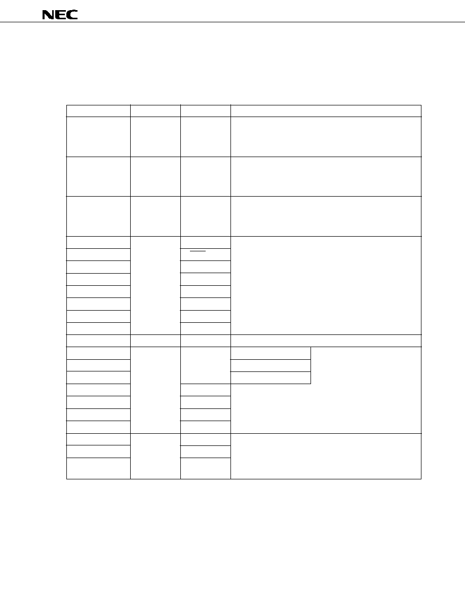
Function List (1/2)
Item
Function
Internal PROM capacity
62 Kbytes
Note
Internal RAM capacity
2048 bytes
Note
Operation clock
16 MHz (Internal clock: 8 MHz)
Low frequency oscillation mode: 8 MHz (Internal clock: 8 MHz)
Low power consumption mode: 32.768 kHz (Subsystem clock)
Minimum instruction execution time
250 ns (at 8-MHz internal clock)
I/O ports
Total: 54
Input: 8
I/O: 46
Real-time output port
11 (including 3 outputs each for Pseudo-V
SYNC
, Head amplifier switch, and Chromi-
nance rotate)
Super
Timer/counter
Timer/counter
Compare register
Capture register
Remark
timer
TM0 (16-bit)
3
≠
unit
TM1 (16-bit)
3
1
FRC (22-bit)
≠
6
TM3 (16-bit)
2
1
UDC (5-bit)
1
≠
EC (8-bit)
4
≠
Generates HSW signal
EDV (8-bit)
1
≠
Divides CFG signal
Capture register
Input signal
Number of bits
Measurement cycle
Operation edge
CFG
22
125 ns to 524 ms
DFG
22
125 ns to 524 ms
HSW
16
1
µ
s to 65.5 ms
V
SYNC
22
125 ns to 524 ms
CTL
16
1
µ
s to 65.5 ms
T
REEL
22
125 ns to 524 ms
S
REEL
22
125 ns to 524 ms
Special circuit for VCR
∑ V
SYNC
separator, H
SYNC
separator
∑ VISS detector, Wide-aspect detector
∑ Field identifier
∑ Head amplifier switch/chrominance rotate output circuit
General purpose timer
Timer
Compare register
Capture register
TM2 (16-bit)
1
≠
TM4 (16-bit)
1 (Capture/compare)
1
TM5 (16-bit)
1
≠
PWM output
∑ 16-bit precision: 3 channels (Carrier frequency: 62.5 kHz)
∑ 8-bit precision: 3 channels (Carrier frequency: 62.5 kHz)
Serial interface
3-wire serial I/O: 2 channels
∑ BUSY/STRB control available (only 1 channel)
A/D converter
8-bit resolution
◊
12 channels, conversion time: 10
µ
s
Note
It is possible to change the capacity of the internal PROM and the internal RAM by specifying the internal
memory capacity select (IMS) register.

4
µ
PD78P4916
Function List (2/2)
Item
Function
Analog unit
∑ CTL amplifier
∑ RECCTL driver (supports re-write operation)
∑ DFG amplifier, DPG comparator, CFG amplifier
∑ DPFG separator (Three-value)
∑ Reel FG comparator (2 channels)
∑ CSYNC comparator
Interrupt
Programmable 4 levels, vectored interrupt, macro service, context switching
External
9 (including NMI)
Internal
19 (including software interrupt)
Standby function
HALT mode/STOP mode
Low-power consumption mode: HALT mode
Release from STOP mode by NMI pin's active edge, Watch interrupt (INTW), or
INTP1/INTP2/KEY0-KEY4 pins' input.
Watch function
0.5-sec interval, capable of low-voltage operation (V
DD
= 2.7 V)
Power supply voltage
V
DD
= 2.7 to 5.5 V
Package
100-pin plastic QFP (14
◊
20 mm)
*
*
µ
PD78P4916
5
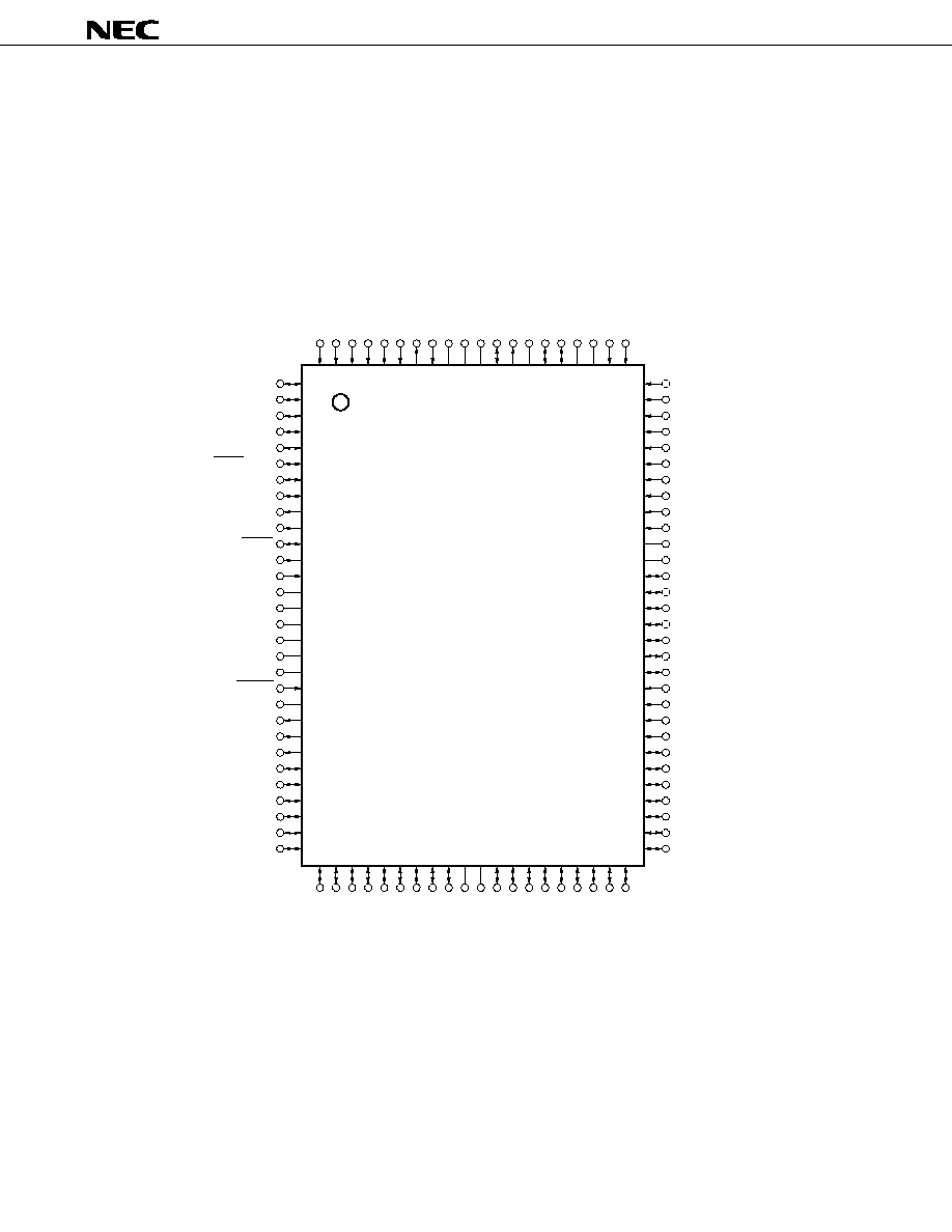
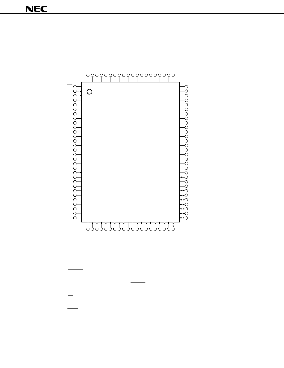
Pin Configuration (Top View)
(1) Normal Operation Mode
∑ 100-pin plastic QFP (14
◊
20 mm)
µ
PD78P4916GF-3BA
Caution Connect the IC (Internally Connected) pin to V
SS
directly.
1
2
3
4
5
6
7
8
9
10
11
12
13
14
15
16
17
18
19
20
21
22
23
24
25
26
27
28
29
30
80
79
78
77
76
75
74
73
72
71
70
69
68
67
66
65
64
63
62
61
60
59
58
57
56
55
54
53
52
51
50
49
48
47
46
45
44
43
42
41
40
39
38
37
36
35
34
33
32
31
81
82
83
84
85
86
87
88
89
90
91
92
93
94
95
96
97
98
99
100
P64
P65/HWIN
P66/PWM4
P67/PWM5
P60/STRB/CLO
P61/SCK1/BUZ
P62/SO1
P63/SI1
PWM0
PWM1
SCK2
SO2
SI2/BUSY
V
DD
XT1
XT2
V
SS
X2
X1
RESET
IC
PTO02
PTO01
PTO00
P87/PTO11
P86/PTO10
P85/PWM3
P84/PWM2
P83/ROTC
P82/HASW
ANI9
ANI8
P77/ANI7
P76/ANI6
P75/ANI5
P74/ANI4
P73/ANI3
P72/ANI2
P71/ANI1
P70/ANI0
AV
REF
AV
DD2
P96
P95/KEY4
P94/KEY3
P93/KEY2
P92/KEY1
P91/KEY0
P90/ENV
NMI
INTP0
INTP1
P00
P01
P02
P03
P04
P05
P06
CSYNCIN
REEL0IN/INTP3
REEL1IN
DFGIN
DPGIN
CFGCPIN
CFGAMPO
CFGIN
AV
DD1
AV
SS1
VREFC
CTLOUT2
CTLOUT1
CTLIN
RECTTL
≠
RECTTL+
CTLDLY
AV
SS2
ANI11
ANI10
P80
P57
P56
P55
P54
P53
P52
P51
P50
V
SS
V
DD
P47
P46
P45
P44
P43
P42
P41
P40
P07
INTP2
6
µ
PD78P4916
ANI0-ANI11
: Analog Input
P00-P07
: Port0
AV
DD1
, AV
DD2
: Analog Power Supply
P40-P47
: Port4
AV
SS1
, AV
SS2
: Analog Ground
P50-P57
: Port5
AV
REF
: Analog Reference Voltage
P60-P67
: Port6
BUSY
: Serial Busy
P70-P77
: Port7
BUZ
: Buzzer Output
P80, P82-P87
: Port8
CFGAMPO
: Capstan FG Amplifier Output
P90-P96
: Port9
CFGCPIN
: Capstan FG Capacitor Input
PTO00-PTO02,
: Programmable Timer Output
CFGIN
: Analog Unit Input
PTO10, PTO11
CLO
: Clock Output
PWM0 - PWM5
: Pulse Width Modulation Output
CSYNCIN
: Analog Unit Input
RECCTL+, RECCTL≠ : RECCTL Output/PBCLT Input
CTLDLY
: Control Delay Input
REEL0IN, REEL1IN : Analog Unit Input
CTLIN
: CTL Amplifier Input Capacitor
RESET
: Reset
CTLOUT1, CTLOUT2 : CTL Amplifier Output
ROTC
: Chrominance Rotate Output
DFGIN
: Analog Unit Input
SCK1, SCK2
: Serial Clock
DPGIN
: Analog Unit Input
SI1, SI2
: Serial Input
ENV
: Envelope Input
SO1, SO2
: Serial Output
HASW
: Head Amplifier Switch Output
STRB
: Serial Strobe
HWIN
: Hardware Timer External Input
V
DD
: Power Supply
IC
: Internally Connected
VREFC
: Reference Amplifier Capacitor
INTP0-INTP3
: Interrupt From Peripherals
Vss
: Ground
KEY0-KEY4
: Key Return
X1, X2
: Crystal (Main System Clock)
NMI
: Nonmaskable Interrupt
XT1, XT2
: Crystal (Subsystem Clock)
µ
PD78P4916
7
Cautions (L)
: Connect to V
SS
via pull-down resistors individually.
V
SS
: Connect to ground.
OPEN : Leave this pin unconnected.
RESET : Apply low level.
A0 - A16 : Address Bus
RESET
: Reset
D0 - D7
: Data Bus
V
DD
: Power Supply
CE
: Chip Enable
V
PP
: Programming Power Supply
OE
: Output Enable
V
SS
: Ground
PGM
: Program
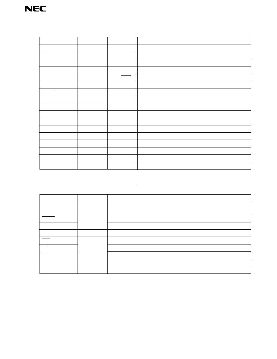
(2) PROM Programming Mode
∑ 100-pin plastic QFP (14
◊
20 mm)
µ
PD78P4916GF-3BA
1
2
3
4
5
6
7
8
9
10
11
12
13
14
15
16
17
18
19
20
21
22
23
24
25
26
27
28
29
30
31 32 33 34 3536 37 38 39 4041 42 43 44 4546 47 48 49 50
80
79
78
77
76
75
74
73
72
71
70
68
67
66
65
64
63
62
61
60
59
58
57
56
55
54
53
52
51
69
10099 98 97 9695 94 93 92 9190 89 88 87 8685 84 83 82 81
OE
CE
PGM
(L)
OPEN
(L)
V
DD
V
SS
OPEN
V
SS
OPEN
V
SS
RESET
IC/V
PP
OPEN
(L)
(L)
OPEN
(L)
V
DD
V
SS
OPEN
OPEN
(L)
(L)
(L)
OPEN
V
SS
(L)
(L)
V
DD
A9
(L)
D0
D1
D2
D3
D4
D5
D6
(L)
A15
A14
A13
A12
A11
A10
A16
A8
V
SS
V
DD
A7
A6
A5
A4
A3
A2
A1
A0
D7
8
µ
PD78P4916
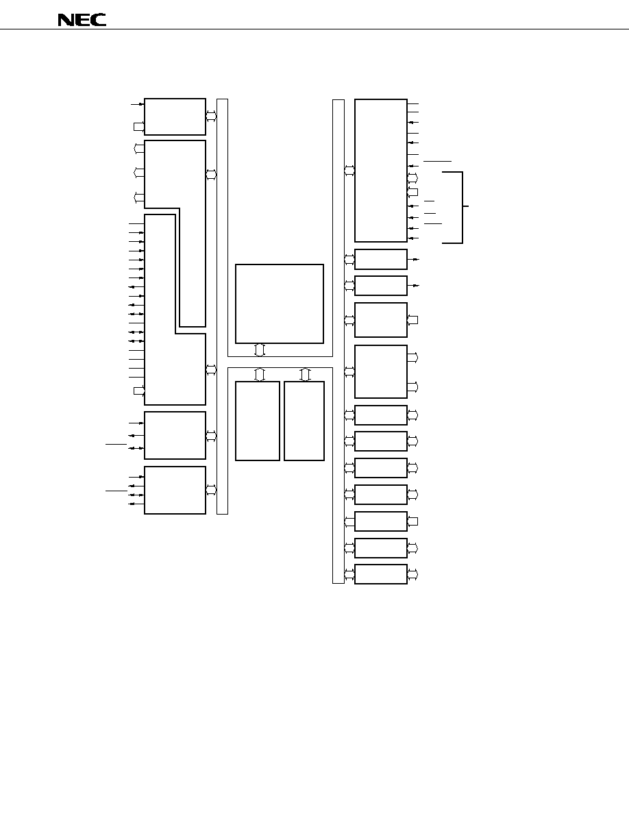
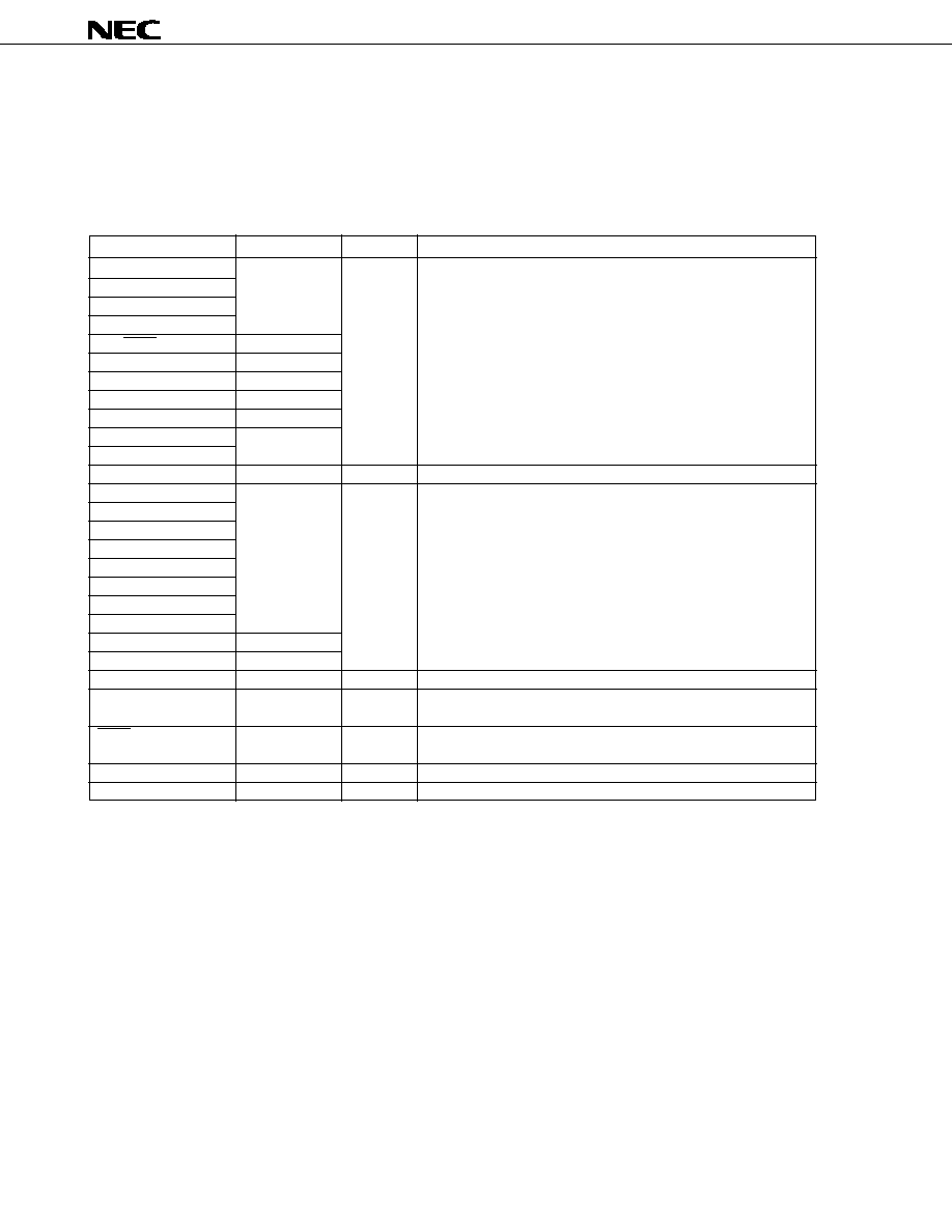
Internal Block Diagram
NMI
ROM
62 Kbytes
D0 - D7
RESET
XT1
X2
X1
V
DD
V
SS
OE
PGM
V
PP
INTP0 -
INTP3
PWM0 -
PWM5
PTO00 -
PTO02
PTO10,
PTO11
VREFC
REEL0IN
REEL1IN
CSYNCIN
DFGIN
DPGIN
CFGIN
CFGAMPO
CFGCPIN
CTLOUT1
CTLOUT2
CTLIN
RECCTL+
RECCTL≠
CTLDLY
AV
DD1
, AV
DD2
AV
SS1
, AV
SS2
AV
REF
ANI0 - ANI11
SI1
SO1
SCK1
SI2/BUSY
SO2
SCK2
STRB
Serial
Interface 2
Serial
Interface 1
Analog Unit
&
A/D Converter
Super Timer
Unit
Interrupt
Control
System
Control
Clock Output
Buzzer Output
Key Input
Real-Time
Output Port
Port4
Port0
Port5
Port6
Port7
Port8
Port9
XT2
A0 - A16
CE
CLO
BUZ
KEY0 - KEY4
P00 - P07
P80, P82, P83
P40 - P47
P00 - P07
P50 - P57
P60 - P67
P70 - P77
P80, P82 - P87
P90 - P96
78K/IV
16-bit CPU Core
(RAM 512 bytes)
RAM
1536 bytes
Used in PROM
programming
mode
µ
PD78P4916
9
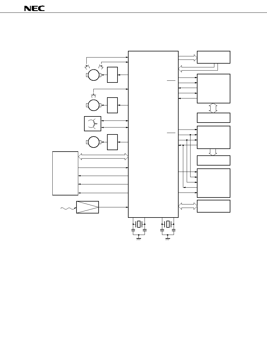
System Configuration Example
∑
Camcorder
Pseudo-vertical sync signal
DFG
DPG
CFG
DFGIN
DPGIN
PWM0
CFGIN
PWM1
PORT
CSYNCIN
PTO00
PTO01
P80
X1
X2
XT1
XT2
PORT
STRB
PORT
BUSY
SO2
SCK2
PORT
INTP0
SO1
SI1
SCK1
PORT
INTP0
SCK
SO
SI
PORT
CS
CLK
DATA
BUSY
LCD C/D
CS
CLK
DATA
BUSY
STB
OSD
PD6456
PD7225
PD78356
PORT
PORT
PD78P4916
M
M
µ
µ
µ
16 MHz
32.768 kHz
Drum motor
Driver
Driver
Capstan motor
Audio-video
signal
processor
Key matrix
Microcontroller
for camera
control
Camera block
LCD display panel
Mechanical block
µ
RECCTL+
CTL head
RECCTL≠
PWM2
M
Driver
Loading motor
INTP2
PC2800A
µ
Remote control
receive signal
Signals from
remote controller
Composite sync signal
Video head switch
Audio head switch

10
µ
PD78P4916
∑
Deck-type VCR
Key matrix
Mechanical block
Tuner unit
DFG
DPG
CFG
DFGIN
DPGIN
PWM0
CFGIN
PWM1
RECCTL+
RECCTL≠
PWM2
PWM4
P80
REEL1IN
X1
X2 XT1
XT2
PORT
PORT
SO1
SI1
PORT
PD78P4916
M
M
M
8 MHz
32.768 kHz
Drum
motor
Driver
Driver
Driver
Capstan
motor
CTL
head
Loading
motor
M
Driver
Reel
motors
M
Driver
REEL0IN
PWM3
PWM5
PTO01
PTO00
CSYNCIN
PORT
Low-frequency
oscillation mode
µ
Reel FG1
Reel FG0
PC2800A
µ
Signals from
remote controller
Remote control
receive signal
INTP2
STB
CLK
DOUT
PD16311
µ
FIP C/D
FIP
DIN
SO2
SCK2
PORT
CS
CLK
DATA
OSD
PD6454
µ
Audio-video
signal
processor unit
Composite
synchronous signal
Video head switch
Audio head switch
Pseudo-vertical
synchronous signal
SCK1
TM

µ
PD78P4916
11
CONTENTS
1. DIFFERENCES BETWEEN
µ
PD78P4916 AND
µ
PD784915,
µ
PD784916A ∑∑∑∑∑∑∑∑∑∑∑∑∑∑∑∑∑∑∑∑∑∑∑∑∑∑∑∑∑∑∑∑∑ 12
2. PIN FUNCTION ∑∑∑∑∑∑∑∑∑∑∑∑∑∑∑∑∑∑∑∑∑∑∑∑∑∑∑∑∑∑∑∑∑∑∑∑∑∑∑∑∑∑∑∑∑∑∑∑∑∑∑∑∑∑∑∑∑∑∑∑∑∑∑∑∑∑∑∑∑∑∑∑∑∑∑∑∑∑∑∑∑∑∑∑∑∑∑∑∑∑∑∑∑∑∑∑∑∑∑∑∑∑∑∑∑∑∑∑∑∑∑∑∑∑∑∑∑∑∑∑∑∑∑∑∑∑∑∑∑ 13
2.1 Normal Operation Mode ∑∑∑∑∑∑∑∑∑∑∑∑∑∑∑∑∑∑∑∑∑∑∑∑∑∑∑∑∑∑∑∑∑∑∑∑∑∑∑∑∑∑∑∑∑∑∑∑∑∑∑∑∑∑∑∑∑∑∑∑∑∑∑∑∑∑∑∑∑∑∑∑∑∑∑∑∑∑∑∑∑∑∑∑∑∑∑∑∑∑∑∑∑∑∑∑∑∑∑∑∑∑∑∑∑∑∑∑∑∑∑∑∑∑∑∑∑∑∑∑∑∑∑∑∑ 13
2.2 PROM Programming Mode (V
PP
5 V, RESET = L) ∑∑∑∑∑∑∑∑∑∑∑∑∑∑∑∑∑∑∑∑∑∑∑∑∑∑∑∑∑∑∑∑∑∑∑∑∑∑∑∑∑∑∑∑∑∑∑∑∑∑∑∑∑∑∑∑∑∑∑∑∑∑∑∑∑∑∑∑∑∑∑∑∑∑∑∑∑∑∑∑∑∑ 15
2.3 Pin I/O Circuits and Recommended Connection of Unused Pins ∑∑∑∑∑∑∑∑∑∑∑∑∑∑∑∑∑∑∑∑∑∑∑∑∑∑∑∑∑∑∑∑∑∑∑∑∑∑∑∑∑∑∑∑∑∑∑∑∑∑∑∑∑∑∑∑∑ 16
3. INTERNAL MEMORY CAPACITY SELECT REGISTER (IMS) ∑∑∑∑∑∑∑∑∑∑∑∑∑∑∑∑∑∑∑∑∑∑∑∑∑∑∑∑∑∑∑∑∑∑∑∑∑∑∑∑∑∑∑∑∑∑∑∑∑∑∑ 20
4. PROM PROGRAMMING ∑∑∑∑∑∑∑∑∑∑∑∑∑∑∑∑∑∑∑∑∑∑∑∑∑∑∑∑∑∑∑∑∑∑∑∑∑∑∑∑∑∑∑∑∑∑∑∑∑∑∑∑∑∑∑∑∑∑∑∑∑∑∑∑∑∑∑∑∑∑∑∑∑∑∑∑∑∑∑∑∑∑∑∑∑∑∑∑∑∑∑∑∑∑∑∑∑∑∑∑∑∑∑∑∑∑∑∑∑∑∑∑∑∑∑ 21
4.1 Operation Mode ∑∑∑∑∑∑∑∑∑∑∑∑∑∑∑∑∑∑∑∑∑∑∑∑∑∑∑∑∑∑∑∑∑∑∑∑∑∑∑∑∑∑∑∑∑∑∑∑∑∑∑∑∑∑∑∑∑∑∑∑∑∑∑∑∑∑∑∑∑∑∑∑∑∑∑∑∑∑∑∑∑∑∑∑∑∑∑∑∑∑∑∑∑∑∑∑∑∑∑∑∑∑∑∑∑∑∑∑∑∑∑∑∑∑∑∑∑∑∑∑∑∑∑∑∑∑∑∑∑∑∑∑∑∑∑∑∑∑ 21
4.2 PROM Write Procedure ∑∑∑∑∑∑∑∑∑∑∑∑∑∑∑∑∑∑∑∑∑∑∑∑∑∑∑∑∑∑∑∑∑∑∑∑∑∑∑∑∑∑∑∑∑∑∑∑∑∑∑∑∑∑∑∑∑∑∑∑∑∑∑∑∑∑∑∑∑∑∑∑∑∑∑∑∑∑∑∑∑∑∑∑∑∑∑∑∑∑∑∑∑∑∑∑∑∑∑∑∑∑∑∑∑∑∑∑∑∑∑∑∑∑∑∑∑∑∑∑∑∑∑∑∑∑ 23
4.3 PROM Read Procedure ∑∑∑∑∑∑∑∑∑∑∑∑∑∑∑∑∑∑∑∑∑∑∑∑∑∑∑∑∑∑∑∑∑∑∑∑∑∑∑∑∑∑∑∑∑∑∑∑∑∑∑∑∑∑∑∑∑∑∑∑∑∑∑∑∑∑∑∑∑∑∑∑∑∑∑∑∑∑∑∑∑∑∑∑∑∑∑∑∑∑∑∑∑∑∑∑∑∑∑∑∑∑∑∑∑∑∑∑∑∑∑∑∑∑∑∑∑∑∑∑∑∑∑∑∑∑ 27
4.4 Screening One-time PROM Versions ∑∑∑∑∑∑∑∑∑∑∑∑∑∑∑∑∑∑∑∑∑∑∑∑∑∑∑∑∑∑∑∑∑∑∑∑∑∑∑∑∑∑∑∑∑∑∑∑∑∑∑∑∑∑∑∑∑∑∑∑∑∑∑∑∑∑∑∑∑∑∑∑∑∑∑∑∑∑∑∑∑∑∑∑∑∑∑∑∑∑∑∑∑∑∑∑∑∑∑∑∑∑∑ 27
5. ELECTRICAL SPECIFICATIONS ∑∑∑∑∑∑∑∑∑∑∑∑∑∑∑∑∑∑∑∑∑∑∑∑∑∑∑∑∑∑∑∑∑∑∑∑∑∑∑∑∑∑∑∑∑∑∑∑∑∑∑∑∑∑∑∑∑∑∑∑∑∑∑∑∑∑∑∑∑∑∑∑∑∑∑∑∑∑∑∑∑∑∑∑∑∑∑∑∑∑∑∑∑∑∑∑∑∑∑∑∑ 28
6. PACKAGE DRAWING ∑∑∑∑∑∑∑∑∑∑∑∑∑∑∑∑∑∑∑∑∑∑∑∑∑∑∑∑∑∑∑∑∑∑∑∑∑∑∑∑∑∑∑∑∑∑∑∑∑∑∑∑∑∑∑∑∑∑∑∑∑∑∑∑∑∑∑∑∑∑∑∑∑∑∑∑∑∑∑∑∑∑∑∑∑∑∑∑∑∑∑∑∑∑∑∑∑∑∑∑∑∑∑∑∑∑∑∑∑∑∑∑∑∑∑∑∑∑ 46
7. RECOMMENDED SOLDERING CONDITIONS ∑∑∑∑∑∑∑∑∑∑∑∑∑∑∑∑∑∑∑∑∑∑∑∑∑∑∑∑∑∑∑∑∑∑∑∑∑∑∑∑∑∑∑∑∑∑∑∑∑∑∑∑∑∑∑∑∑∑∑∑∑∑∑∑∑∑∑∑∑∑∑∑∑∑∑∑∑∑∑∑∑ 47
APPENDIX A. DEVELOPMENT TOOLS ∑∑∑∑∑∑∑∑∑∑∑∑∑∑∑∑∑∑∑∑∑∑∑∑∑∑∑∑∑∑∑∑∑∑∑∑∑∑∑∑∑∑∑∑∑∑∑∑∑∑∑∑∑∑∑∑∑∑∑∑∑∑∑∑∑∑∑∑∑∑∑∑∑∑∑∑∑∑∑∑∑∑∑∑∑∑∑∑∑∑∑∑∑ 48
APPENDIX B. SOCKET DRAWING AND RECOMMENDED FOOTPRINT ∑∑∑∑∑∑∑∑∑∑∑∑∑∑∑∑∑∑∑∑∑∑∑∑∑∑∑∑∑∑∑∑∑∑∑∑∑∑∑∑ 50
APPENDIX C. RELATED DOCUMENTS ∑∑∑∑∑∑∑∑∑∑∑∑∑∑∑∑∑∑∑∑∑∑∑∑∑∑∑∑∑∑∑∑∑∑∑∑∑∑∑∑∑∑∑∑∑∑∑∑∑∑∑∑∑∑∑∑∑∑∑∑∑∑∑∑∑∑∑∑∑∑∑∑∑∑∑∑∑∑∑∑∑∑∑∑∑∑∑∑∑∑∑∑ 52
*
*
*
*
12
µ
PD78P4916
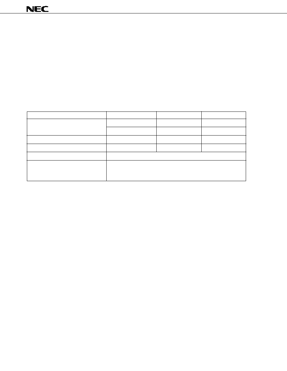
1. DIFFERENCES BETWEEN
µ
PD78P4916 AND
µ
PD784915,
µ
PD784916A
Other than the memory types, their capacities, and memory-related points, the functions of the three devices are
identical: the
µ
PD78P4916 incorporates a one-time PROM that is rewritable by users, while the
µ
PD784915 and
784916A contain mask ROMs.
Table 1-1 shows the differences among these devices. Be sure to keep in mind these differences especially when
debugging and pre-producing the application system with the PROM version and then mass-producing it with the
mask-ROM version.
For the details about the CPU functions and on-chip hardware, refer to the
µ
PD784915 Subseries User's
Manual--Hardware (U10444E).
Table 1-1. Differences among
µ
PD784915 Subseries Devices
Parameters
µ
PD78P4916
µ
PD784915
µ
PD784916A
Internal ROM
One-time PROM
Mask ROM
Mask ROM
62 Kbytes
Note
48 Kbytes
62 Kbytes
Internal RAM
2048 bytes
Note
1280 bytes
1280 bytes
Internal memory size select register (IMS)
Provided
Not provided
Not provided
Pinouts
Pins related to PROM writing and reading are provided on the
µ
PD78P4916.
Other
There are differences in noise immunity, noise radiation, and some electrical
specifications, because of the differences in circuit complexity and mask
layout.
Note
The internal PROM and RAM capacities of the
µ
PD78P4916 can be changed through its internal memory
size select register (IMS).
Caution There are differences in noise immunity and noise radiation between the PROM and mask-ROM
versions. When pre-producing the application set with the PROM version and then mass-
producing it with the mask-ROM version, be sure to conduct sufficient evaluations for the set
using consumer samples (not engineering samples) of the mask-ROM version.
*
µ
PD78P4916
13
2.
PIN FUNCTION
2.1 Normal Operation Mode
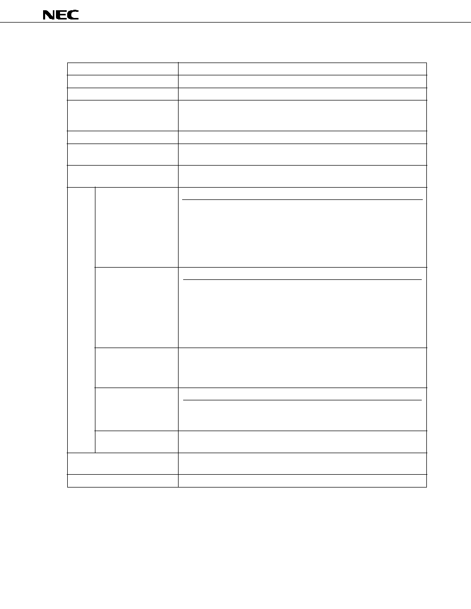
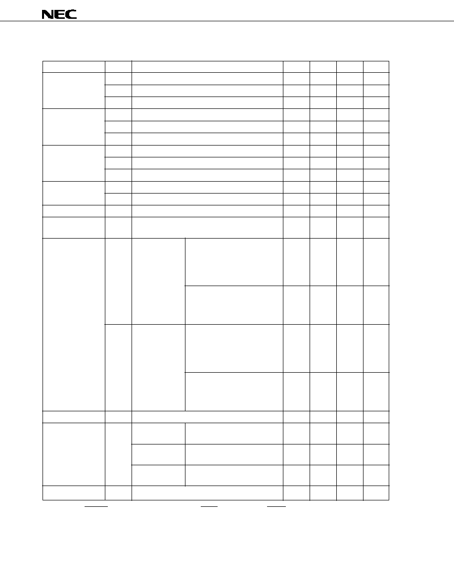
(1) Port Pins
Pin Name
Input/Output
Alternate function
Description
P00 - P07
I/O
Real-time
8-bit input/output port (Port0)
output port
∑ Specifiable to input or output mode bitwise.
∑ With software-specifiable on-chip pull-up resistors
(P00 - P07).
P40 - P47
I/O
≠
8-bit input/output port (Port4)
∑ Specifiable to input or output mode bitwise.
∑ With software-specifiable on-chip pull-up resistors
(P40 - P47).
P50 - P57
I/O
≠
8-bit input/output port (Port5)
∑ Specifiable to input or output mode bitwise.
∑ With software-specifiable on-chip pull-up resistors
(P50 - P57).
P60
I/O
STRB/CLO
8-bit input/output port (Port6)
P61
SCK1/BUZ
∑ Specifiable to input or output mode bitwise.
P62
SO1
∑ With software-specifiable on-chip pull-up resistors
P63
SI1
(P60 - P67).
P64
≠
P65
HWIN
P66
PWM4
P67
PWM5
P70 - P77
Input
ANI0 - ANI7
8-bit input port (Port7)
P80
I/O
Real-time
for Pseudo-V
SYNC
output
7-bit input/output port (Port8)
P82
output port
for HASW output
∑ Specifiable to input or output
P83
for ROTC output
mode bitwise.
P84
PWM2
∑ With software-specifiable on-chip
P85
PWM3
pull-up resistors (P80, P82 - P87)
P86
PTO10
P87
PTO11
P90
I/O
ENV
7-bit input/output port (Port9)
P91 - P95
KEY0 - KEY4
∑ Specifiable to input or output mode bitwise.
P96
≠
∑ With software-specifiable on-chip pull-up resistors
(P90 - P96).
14
µ
PD78P4916
(2) Non-Port Pins (1/2)
Pin Name
Input/Output
Alternate function
Description
REEL0IN
Input
INTP3
Reel FG inputs
REEL1IN
≠
DFGIN
≠
Drum FG, PFG input (Three-value)
DPGIN
≠
Drum PG input
CFGIN
≠
Capstan FG input
CSYNCIN
≠
Composite SYNC input
CFGCPIN
≠
CFG comparator input
CFGAMPO
Output
≠
CFG amplifier output
PTO00
Output
≠
Programmable timer outputs of super timer unit
PTO01
≠
PTO02
≠
PTO10
P86
PTO11
P87
PWM0
Output
≠
PWM outputs of super timer unit
PWM1
≠
PWM2
P84
PWM3
P85
PWM4
P66
PWM5
P67
HASW
Output
P82
Head amplifier switch output
ROTC
Output
P83
Chrominance rotate output
ENV
Input
P90
Envelope input
SI1
Input
P63
Serial data input (Serial interface channel 1)
SO1
Output
P62
Serial data output (Serial interface channel 1)
SCK1
I/O
P61/BUZ
Serial clock input/output (Serial interface channel 1)
SI2
Input
BUSY
Serial data input (Serial interface channel 2)
SO2
Output
≠
Serial data output (Serial interface channel 2)
SCK2
I/O
≠
Serial clock input/output (Serial interface channel 2)
BUSY
Input
SI2
Serial busy input (Serial interface channel 2)
STRB
Output
P60/CLO
Serial strobe output (Serial interface channel 2)
ANI0 - ANI7
Analog inputs
P70 - P77
Analog inputs for A/D converter
ANI8 - ANI11
≠
CTLIN
≠
≠
CTL amplifier input capacitor
CTLOUT1
Output
≠
CTL amplifier output
CTLOUT2
I/O
≠
Logic input/CTL amplifier output
RECCTL+, RECCTL≠
I/O
≠
RECCTL output/PBCTL input
CTLDLY
≠
≠
External time-constant connection (to rewrite RECCTL)
VREFC
≠
≠
AC ground for VREF amplifier
NMI
Input
≠
Non-maskable interrupt request input
µ
PD78P4916
15
(2) Non-Port Pins (2/2)
Pin Name
Input/Output
Alternate function
Description
INTP0 - INTP2
Input
≠
External interrupt request input
INTP3
Input
REEL0IN
KEY0 - KEY4
Input
P91 - P95
Key input signal
CLO
Output
P60/STRB
Clock output
BUZ
Output
P61/SCK1
Buzzer output
HWIN
Input
P65
Hardware timer external input
RESET
Input
≠
Reset input
X1
Input
≠
Crystal resonator connection for main system clock oscillation
X2
≠
XT1
Input
≠
Crystal resonator connection for subsystem clock oscillation
XT2
≠
Crystal resonator connection for clock oscillation of watch
AV
DD1
, AV
DD2
≠
≠
Positive power supply for analog unit
AV
SS1
, AV
SS2
≠
≠
GND for analog unit
AV
REF
≠
≠
Reference voltage input to A/D converter
V
DD
≠
≠
Positive power supply to digital unit
V
SS
≠
≠
GND of digital unit
IC
≠
≠
Internally connected. Connect directly to V
SS
.
2.2 PROM Programming Mode (V
PP
5 V, RESET = L)
Pin name
Input/output
Function
V
PP
≠
Set PROM programming mode
High voltage applied at program write/verify operation
RESET
Input
Low level input for setting PROM programming mode
A0 - A16
Address input
D0 - D7
I/O
Data input/output
PGM
Input
Program inhibit input in PROM programming mode
CE
PROM enable input / programming pulse input
OE
Read strobe input to PROM
V
DD
≠
Positive power supply
V
SS
GND potential
16
µ
PD78P4916
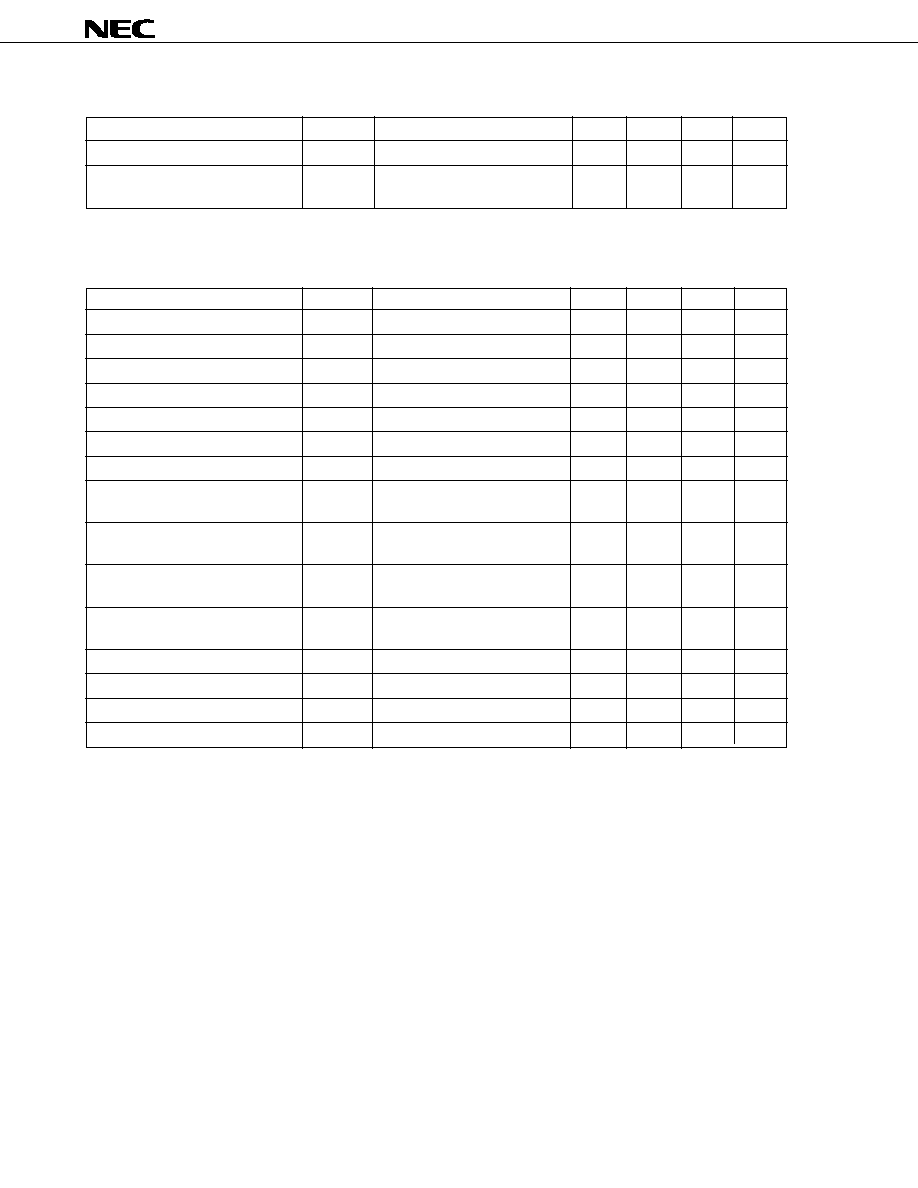
2.3 Pin I/O Circuits and Recommended Connection of Unused Pins
Table 2-1 shows the input/output circuit types of the device's pins and the recommended connection
of the pins which are unnecessary to the user's application. The circuit diagrams for the I/O circuits are
shown in Figure 2-1.
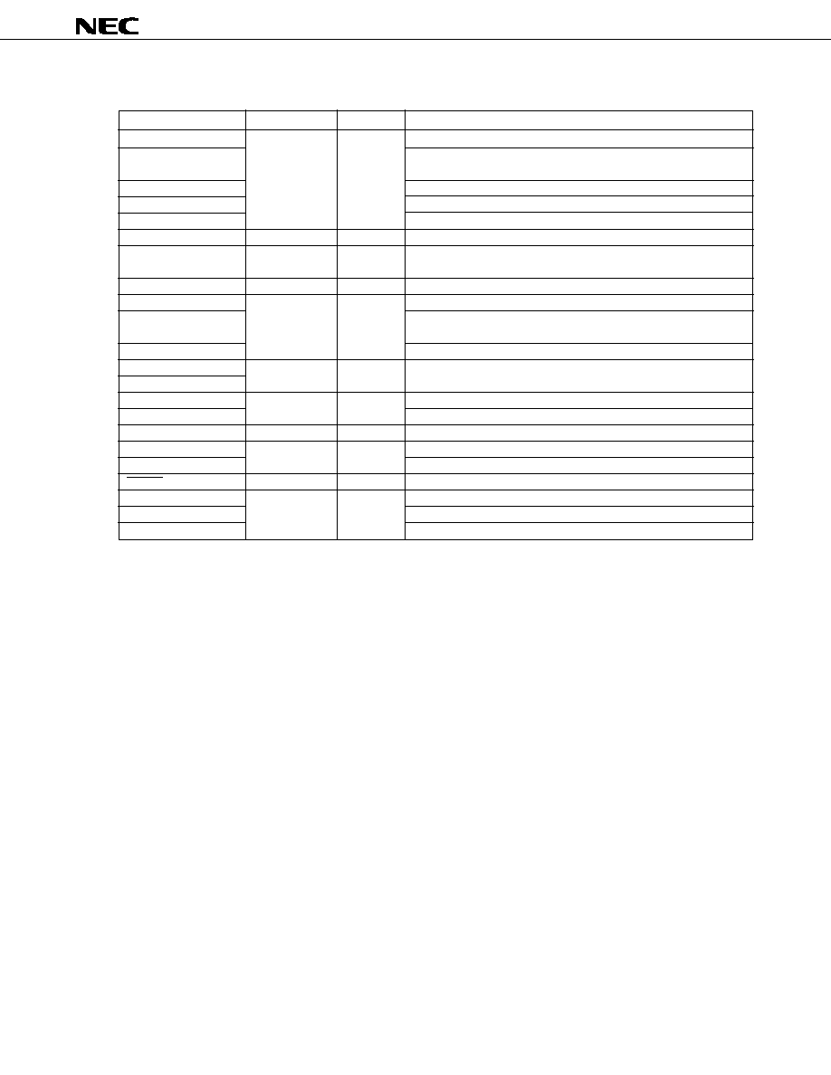
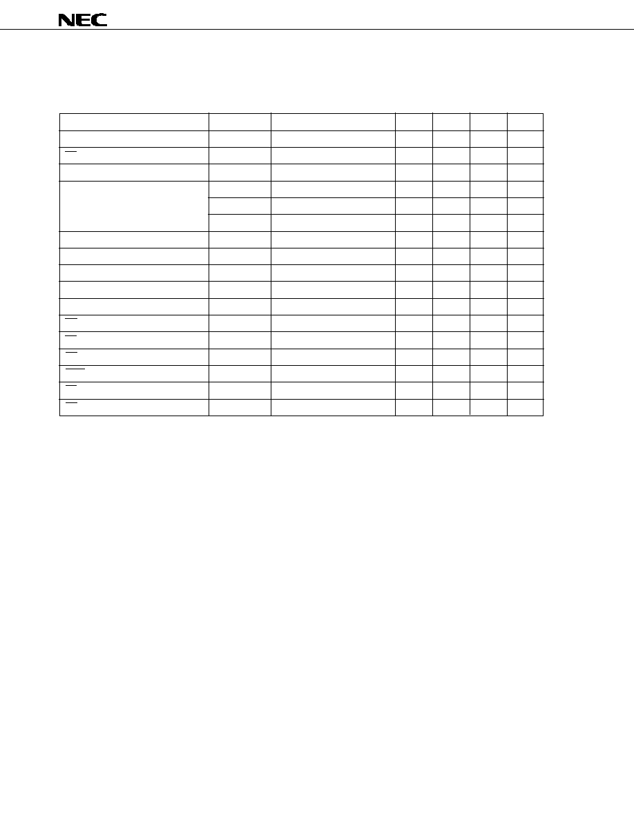
Table 2-1. Pin I/O Circuits and Recommended Connection of Unused Pins (1/2)
Pins
I/O circuit types
Direction
Recommended connection of unused pins
P00-P07
5-A
I/O
Input mode: Connect to V
DD
.
P40-P47
Output mode: Leave unconnected.
P50-P57
P60/STRB/CLO
P61/SCK1/BUZ
8-A
P62/SO1
5-A
P63/SI1
8-A
P64
5-A
P65/HWIN
8-A
P66/PWM4
5-A
P67/PWM5
P70/ANI0-P77/ANI7
9
Input
Connect to V
SS
.
P80
5-A
I/O
Input mode: Connect to V
DD
.
P82/HASW
Output mode: Leave unconnected.
P83/ROTC
P84/PWM2
P85/PWM3
P86/PTO10
P87/PTO11
P90/ENV
P91/KEY0-P95/KEY4
8-A
P96
5-A
SI2/BUSY
2-A
Input
Connect to V
DD
.
SO2
4
Output
High-impedance mode: Connect to V
SS
via a pull-down resistor.
Otherwise: Leave unconnected.
SCK2
8-A
I/O
Input mode: Connect to V
DD
.
Output mode: Leave unconnected.
ANI8-ANI11
7
Input
Connect to V
SS
.
RECCTL+, RECCTL≠
--
I/O
When ENCTL = 0 and ENREC = 0: Connect to V
SS
.
Remark ENCTL: Bit 1 of the amplifier control register (AMPC)
ENREC: Bit 7 of the amplifier mode register 0 (AMPM0)
*
µ
PD78P4916
17
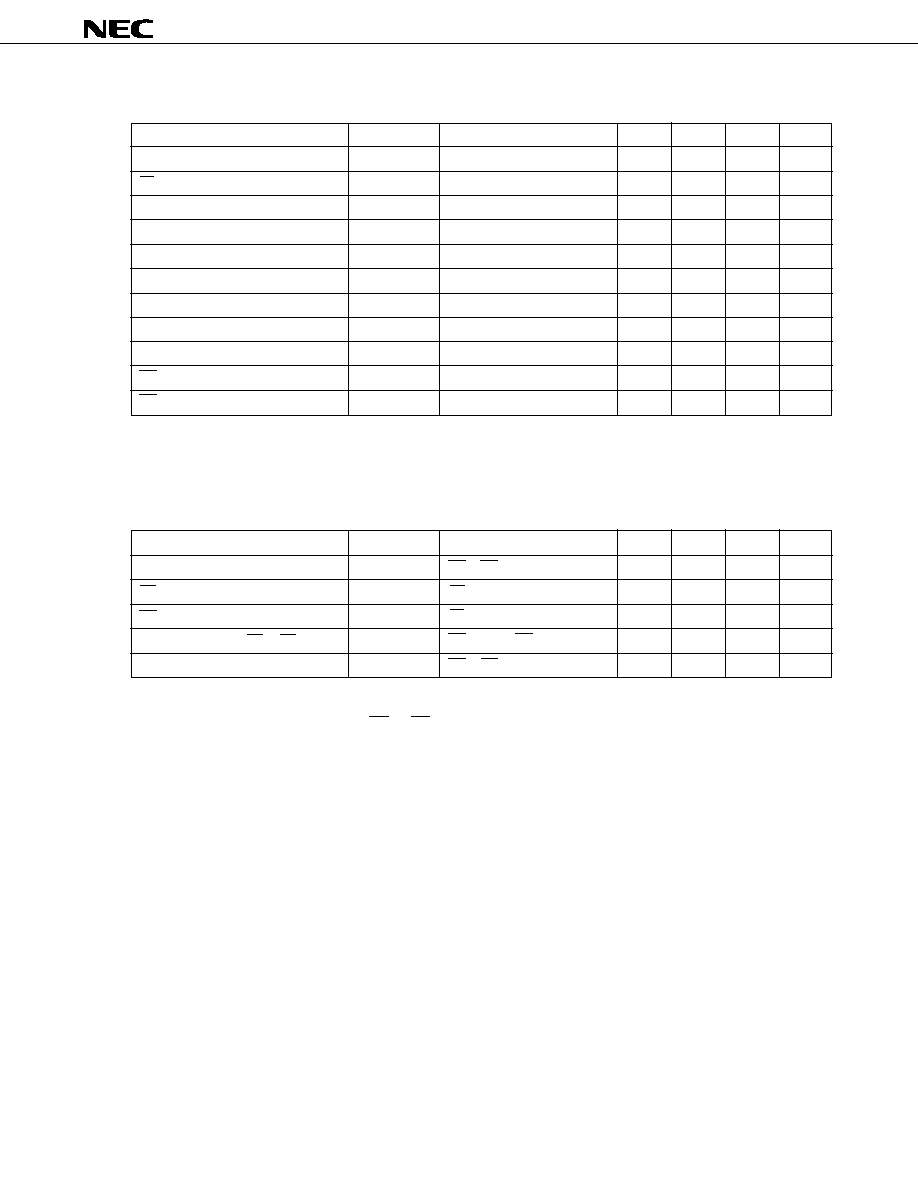
Table 2-1. Pin I/O Circuits and Recommended Connection of Unused Pins (2/2)
Pins
I/O circuit types
Direction
Recommended connection of unused pins
DFGIN
--
Input
ENDRUM = 0: Connect to V
SS
.
DPGIN
ENDRUM = 0, or ENDRUM = 1 and SELPGSEPA = 0:
Connect to V
SS
.
CFGIN, CFGCPIN
ENCAP = 0: Connect to V
SS
.
CSYNCIN
ENCSYN = 0: Connect to V
SS
.
REEL0IN/INTP3, REEL1IN
ENREEL = 0: Connect to V
SS
.
CTLOUT1
--
Output
Leave unconnected.
CTLOUT2
--
I/O
When ENCTL and ENCOMP = 0 and 0: Connect to V
SS
.
ENCTL = 1: Leave unconnected.
CFGAMPO
--
Output
Leave unconnected.
CTLIN
--
--
When ENCTL = 0: Leave unconnected.
VREFC
When ENCTL, ENCAP, and ENCOMP = 0, 0, and 0:
Leave unconnected.
CTLDLY
Leave unconnected.
PWM0, PWM1
3
Output
Leave unconnected.
PTO00-PTO02
NMI
2
Input
Connect to V
DD
.
INTP0
Connect to V
DD
or V
SS
.
INTP1, INTP2
2-A
Input
Connect to V
DD
.
AV
DD1
, AV
DD2
--
--
Connect to V
DD
.
AV
REF
, AV
SS1
, AV
SS2
Connect to V
SS
.
RESET
2
--
--
XT1
--
--
Connect to V
SS
.
XT2
Leave unconnected.
IC
Connect directly to V
SS
.
Remark
ENDRUM:
Bit 2 of the amplifier control register (AMPC)
SELPGSEPA: Bit 2 of the amplifier mode register 0 (AMPM0)
ENCAP:
Bit 3 of the amplifier control register (AMPC)
ENCSYN:
Bit 5 of the amplifier control register (AMPC)
ENREEL:
Bit 6 of the amplifier control register (AMPC)
ENCTL:
Bit 1 of the amplifier control register (AMPC)
ENCOMP:
Bit 4 of the amplifier control register (AMPC)
18
µ
PD78P4916
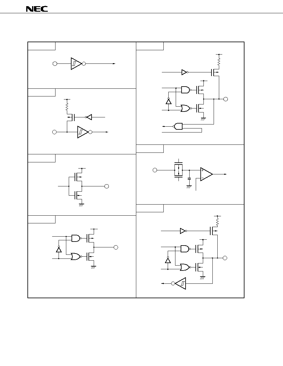
Figure 2-1. Pin I/O Circuit Diagrams (1/2)
IN
Schmitt triggered input with hysteresis characteristics.
IN
V
DD
P-ch
pullup
enable
data
P-ch
N-ch
OUT
V
DD
V
DD
P-ch
N-ch
OUT
data
output
disable
Push-pull output that can also set the output to the
high-impedance state
(both P-ch and N-ch transistors are turned off.)
V
DD
P-ch
N-ch
P-ch
V
DD
IN/
OUT
pullup
enable
data
output
disable
P-ch
N-ch
V
REF
(Threshold voltage)
IN
Comparator
V
DD
P-ch
N-ch
IN/
OUT
data
output
disable
V
DD
P-ch
pullup
enable
input
enable
Type 2
Type 2-A
Type 3
Type 4
Type 8-A
Type 7
Type 5-A
Schmitt triggered input with hysteresis characteristics.

µ
PD78P4916
19
Figure 2-1. Pin I/O Circuit Diagrams (2/2)
Comparator
V
REF
(Threshold voltage)
N-ch
P-ch
IN
input enable
Type 9

20
µ
PD78P4916
3.
INTERNAL MEMORY CAPACITY SELECT REGISTER (IMS)
Internal memory capacity select register (IMS) specifies the effective area of on-chip memory (PROM, RAM) of
the
µ
PD78P4916. Setting this register is required when the capacity of the ROM or RAM in the mask version is
smaller than that of the
µ
PD78P4916. If the memory capacity of the
µ
PD78P4916 is appropriately defined using
this register, bugs in application programs due to accessing an address beyond the memory capacity of the actual
chip can be avoided.
The IMS register is write-only register. To write this register, use the 8-bit manipulation instruction.
The register is initialized to FFH by RESET input (ROM: 62 Kbytes, RAM: 2048 bytes).
Figure 3-1. Internal Memory Capacity Select Register (IMS) Format
Caution The
µ
PD78P4916 has the IMS and the
µ
PD784915 and 784916A do not have it. However, if a
write instruction to IMS is executed in the
µ
PD784915 or 784916A, it does not cause conflicts
or malfunctions.
7
6
5
4
2
3
1
0
1
1
1
ROM1 ROM0
1
RAM1 RAM0
IMS
FFFCH
FFH
W
R/W
State at reset
Address
RAM1 RAM0
0
1
1
1
Specification of internal RAM capacity
1280 bytes
2048 bytes
Setting prohibited
ROM1 ROM0
1
1
0
1
Specification of internal ROM capacity
48 Kbytes
62 Kbytes
Other
Setting prohibited
Other
*
µ
PD78P4916
21
4.
PROM PROGRAMMING
The
µ
PD78P4916 has on-chip 62-Kbyte PROM as the program memory. The PROM programming mode is
entered by setting V
DD
, IC/V
PP
, and RESET pins as specified. For the settings of the unused pins in this mode,
refer to the drawing of "(2) PROM Programming Mode" in the section "Pin Configuration (Top View)".
4.1 Operation Mode
The PROM programming mode is entered by applying +5 V or +12 V to the IC/V
PP
pin, +5 V or +6.5 V to the V
DD
pins, and low-level voltage to the RESET pin. Table 4-1 shows the operation mode specified by the CE, OE, and
PGM pins.
It is possible to read the contents of PROM by setting up read operation mode.
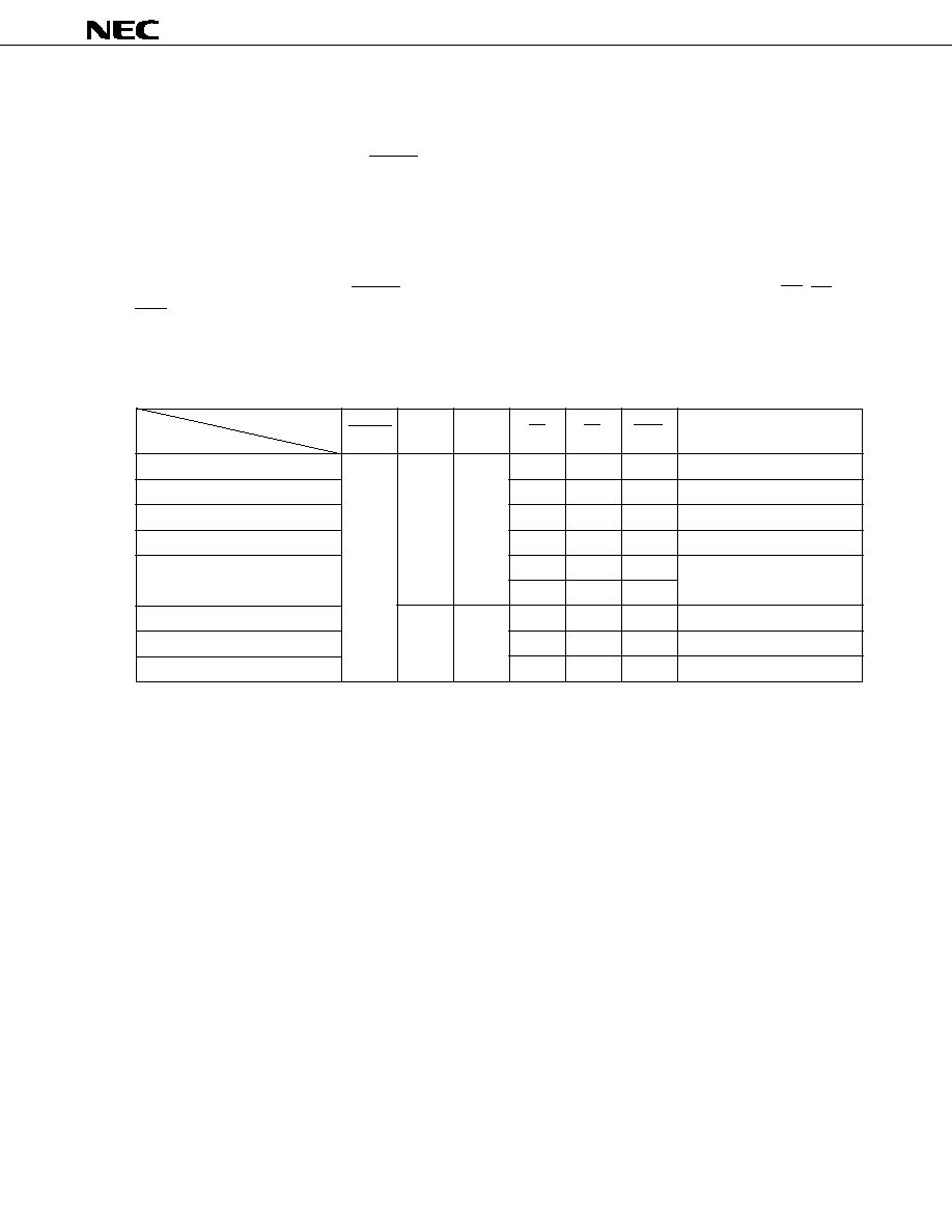
Table 4-1. Operation Mode of PROM Programming
P i n s
RESET
IC/V
PP
V
DD
CE
OE
PGM
D0 - D7
Operation mode
Page data latch
L
+12.5 V
+6.5 V
H
L
H
Data input
Page write
H
H
L
High impedance
Byte write
L
H
L
Data input
Program verify
L
L
H
Data output
Program inhibit
◊
H
H
High impedance
◊
L
L
Read
+5 V
+5 V
L
L
H
Data output
Output disable
L
H
◊
High impedance
Standby
H
◊
◊
High impedance
Remark
◊
: Low or high level

22
µ
PD78P4916
(1) Read mode
By setting CE = L and OE = L, the device enters the read mode.
(2) Output disable mode
By setting OE = H, the device enters the output disable mode, where data output pins go to high impedance
state.
Therefore it is possible to read data from a specified device by enabling only the OE pin of the device to be
read, if two or more
µ
PD78P4916s are connected to a data bus.
(3) Standby mode
By setting CE = H, the device enters the Standby mode.
In this mode, data output pins go to high impedance state regardless of the OE pin condition.
(4) Page data latch mode
By setting CE = H, PGM = H, and OE = L at the beginning of page programming mode, the device enters the
page data latch mode.
In this mode, 4-byte data are latched in page units (consisting of 4 bytes) to internal address/data latch circuit.
(5) Page programming mode
After one-page data (consisting of 4 bytes) and their address are latched in the page data latch mode, the page
programming operation is executed by applying 0.1-ms programming pulse (active low) to the PGM pin under
CE = H, OE = H conditions. Following that operation, the programming data is verified by setting CE = L and
OE = L.
When data is not programmed by one programming pulse, the write and verify operations are repeated X times
(X
10).
(6) Byte programming mode
Applying 0.1-ms programming pulse (active low) to the PGM pin under CE = L and OE = H condition, byte
programming operation is executed. Next, the programming data is verified by setting OE = L.
When data is not programmed by one programming pulse, the write and verify operations are repeated X times
(X
10).
(7) Program verify mode
By setting CE = L, PGM = H, and OE = L, the device enters the program verify mode. Check whether data
is programmed correctly or not in this mode after write operation.
(8) Program inhibit mode
When the OE pins, V
PP
pins, and D0-D7 pins of two or more
µ
PD78P4916s are connected in parallel, use
program inhibit mode to write data to one of those devices.
Programming is executed in the page programming mode or byte programming mode as mentioned above. At
that time, data is not programmed to a device for which high level voltage is applied to the PGM pin.
µ
PD78P4916
23
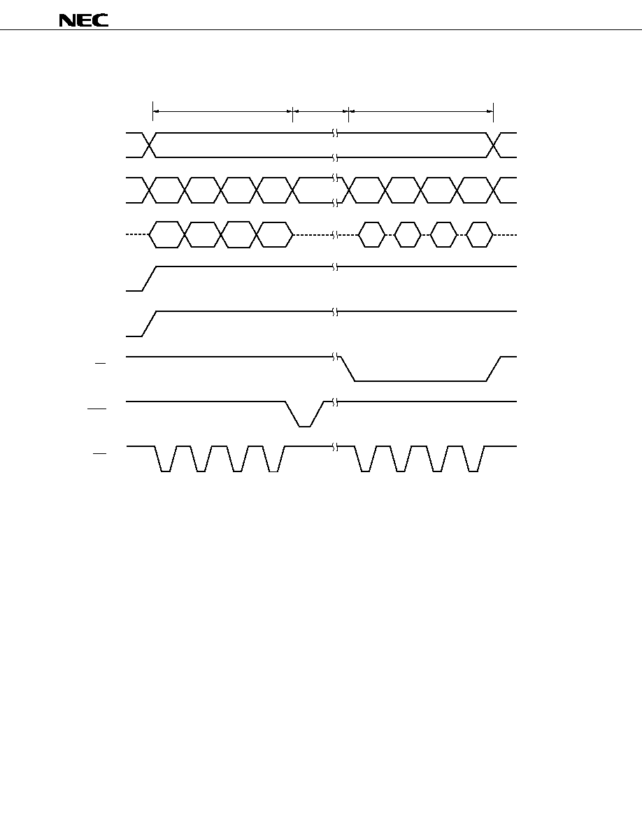
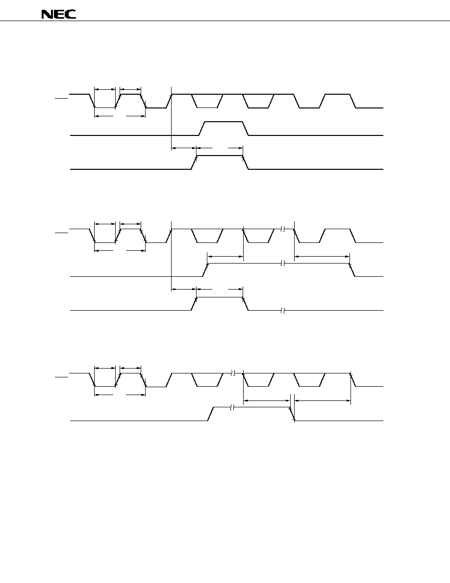
4.2 PROM Write Procedure
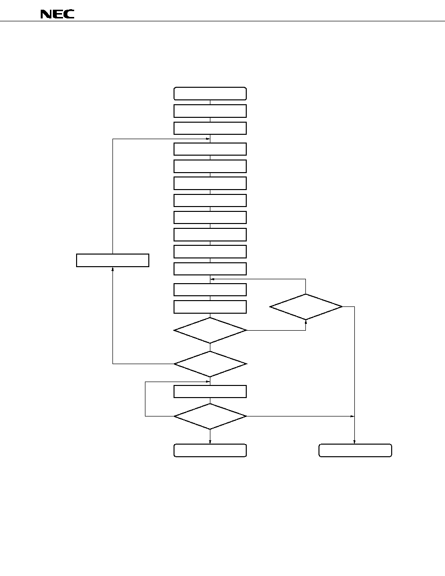
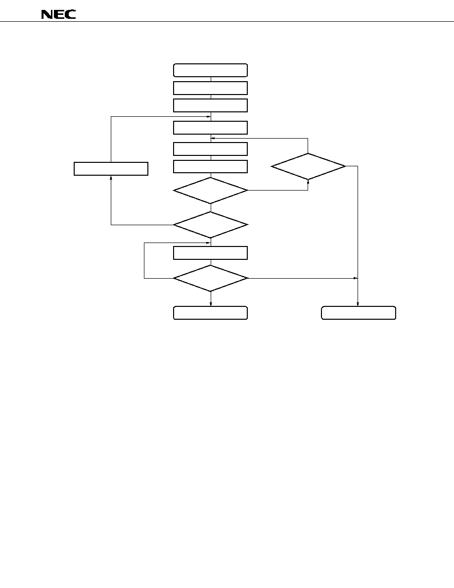
Figure 4-1. Flowchart in Page Programming Mode
Remarks 1. G = Start address
2. N = End address of the program
Start
Address = G
V
DD
= 6.5 V, V
PP
= 12.5 V
X = 0
Latch
Address = Address + 1
Latch
Address = Address + 1
Latch
Address = Address + 1
Latch
X = X+1
0.1-ms programming pulse
Verify 4 bytes
Pass
Fail
Address = N ?
Yes
V
DD
= 4.5 to 5.5 V, V
PP
= V
DD
Fail
Pass
No
All Pass
Verify all bytes
Write operation end
Defective
X = 10?
Yes
No
Address = Address + 1
24
µ
PD78P4916
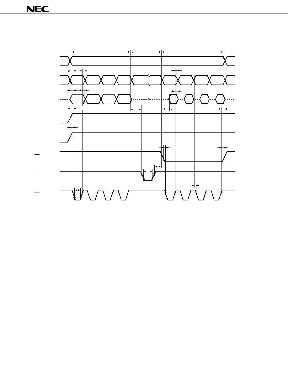
Figure 4-2. Operation Timing in Page Programming Mode
Page data latch
Page programming
Program verify
Address input
Address input
Hi-Z
Data input
Data output
Hi-Z
Hi-Z
D0 - D7
A0, A1
A2 - A16
V
PP
V
PP
V
DD
V
DD
+1.5
V
DD
V
DD
V
IH
CE
V
IL
V
IH
V
IL
V
IH
V
IL
PGM
OE
µ
PD78P4916
25
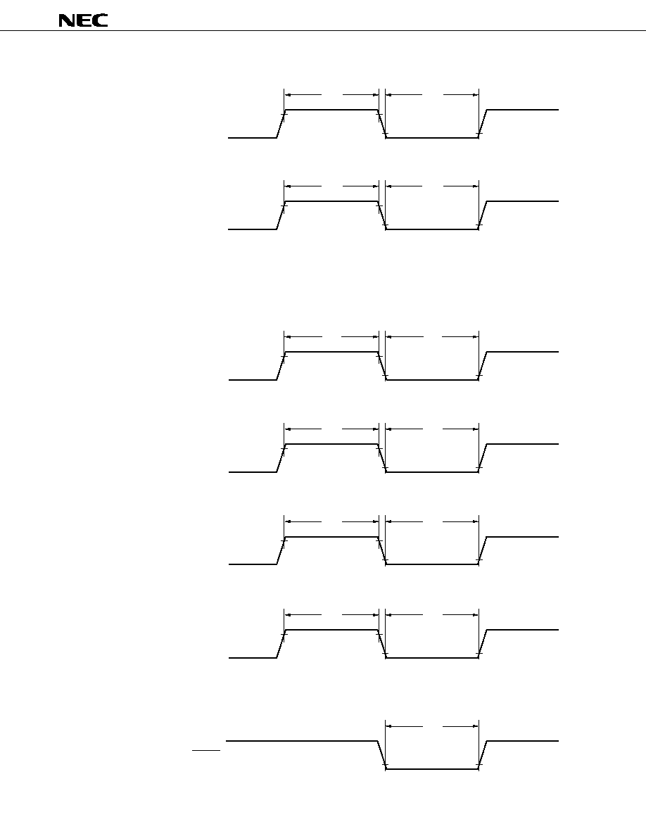
Figure 4-3. Flowchart in Byte Programming Mode
Remarks 1. G = Start address
2. N = End address of the program
V
DD
= 6.5 V, V
PP
= 12.5 V
Address = G
X = 0
X = X+1
0.1-ms programming pulse
Verify
Pass
Fail
Address = N ?
Yes
V
DD
= 4.5 to 5.5 V, V
PP
= V
DD
Fail
Pass
No
All Pass
Verify all bytes
Write operation end
Defective
X = 10?
Yes
No
Address = Address + 1
Start
26
µ
PD78P4916
Programming
Program verify
Address input
Hi-Z
Data input
Data output
Hi-Z
Hi-Z
D0 - D7
A0 - A16
V
PP
V
PP
V
DD
V
DD
+1.5
V
DD
V
DD
V
IH
CE
V
IL
V
IH
V
IL
V
IH
V
IL
PGM
OE
Figure 4-4. Operation Timing in Byte Programming Mode
Cautions 1. Apply voltage to V
DD
before applying voltage to V
PP
, and cut off V
DD
voltage after V
PP
voltage
is cut off.
2. The voltage including overshoot applied to V
PP
pin must be kept less than +13.5 V.
3. If a device is inserted or removed while +12.5 V is applied to V
PP
pin, it may be adversely
affected in reliability.

µ
PD78P4916
27
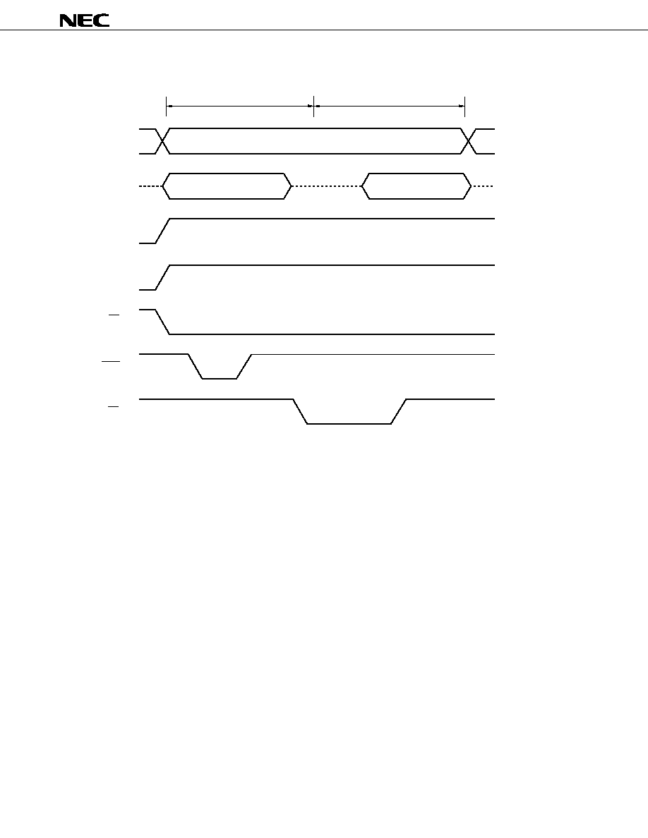
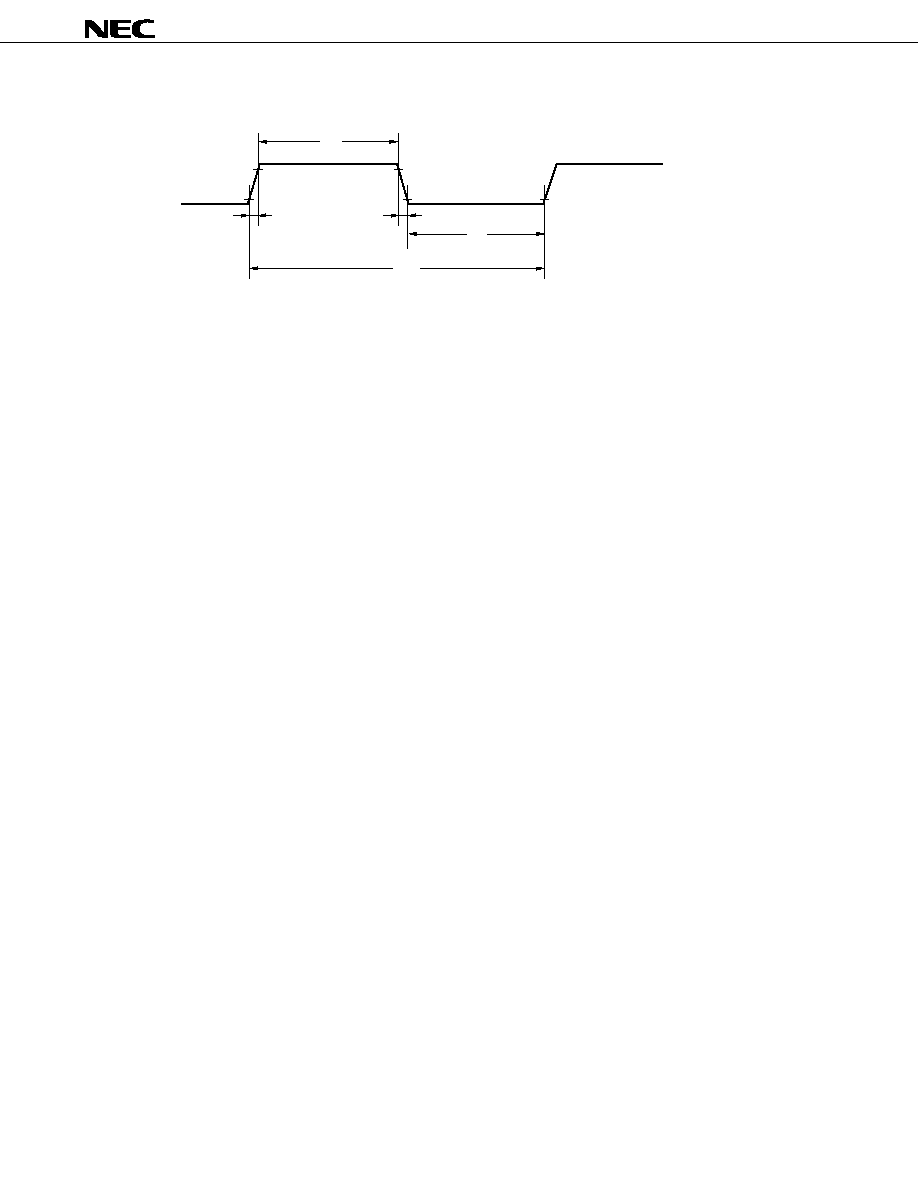
4.3 PROM Read Procedure
The contents of PROM can be read onto external data bus (D0-D7) as described below:
(1) Fix RESET pin to low and supply +5 V to V
PP
pin. Connect other unused pins as specified in "(2) PROM
Programming Mode" in section "Pin Configuration (Top View)."
(2) Supply +5 V to the V
DD
and V
PP
pins.
(3) Input the address of the data to be read to the A0-A16 pins.
(4) Enter the read mode (CE = L, OE = L).
(5) Output data to D0-D7 pins.
The above operation timing from (2) to (5) is shown in Figure 4-5.
Figure 4-5. PROM Read Timing
4.4 Screening One-time PROM Versions
The one-time PROM version (
µ
PD78P4916GF-3BA) cannot be completely tested by NEC for shipment because
of its structure. For screening, it is recommended to verify PROM after storing the necessary data under the following
conditions:
Storage Temperature
Storage Time
125 ∞C
24 hours
Address input
Hi-Z
Data output
Hi-Z
D0 - D7
A0 - A16
OE (Input)
CE (Input)
28
µ
PD78P4916
5.
ELECTRICAL SPECIFICATIONS
Absolute Maximum Ratings (T
A
= 25 ∞C)
Parameter
Symbol
Conditions
Ratings
Unit
Supply voltage
V
DD
V
DD
≠ AV
DD1
0.5 V
≠0.5 to +7.0
V
AV
DD1
V
DD
≠ AV
DD2
0.5 V
≠0.5 to +7.0
V
AV
DD2
AV
DD1
≠ AV
DD2
0.5 V
≠0.5 to +7.0
V
AV
SS1
≠0.5 to +0.5
V
AV
SS2
≠0.5 to +0.5
V
Input voltage
V
I
≠0.5 to V
DD
+0.5
V
Analog input voltage
V
IAN
V
DD
AV
DD2
≠0.5 to AV
DD2
+0.5
V
(ANI0-ANI11)
V
DD
< AV
DD2
≠0.5 to V
DD
+0.5
V
Output voltage
V
O
≠0.5 to V
DD
+0.5
V
Output current, low
I
OL
Per pin
15
mA
Total of all output pins
100
mA
Output current, high
I
OH
Per pin
≠10
mA
Total of all output pins
≠50
mA
Operating ambient
T
A
≠10 to +70
∞C
temperature
Storage temperature
T
stg
≠65 to +150
∞C
Caution If any of the above parameters exceeds the absolute maximum ratings, even momentarily,
device reliability may be impaired. The absolute maximum ratings are values that may
physically damage the product. Be sure to use the product within the ratings.
Operating Conditions
Clock frequency
Operating ambient
Operating condition
Supply voltage (V
DD
)
temperature (T
A
)
4 MHz
f
XX
16 MHz
≠10 to +70 ∞C
All functions
+4.5 to +5.5 V
CPU function only
+4.0 to +5.5 V
32 kHz
f
XT
35 kHz
Subclock operation (CPU, watch,
+2.7 to +5.5 V
and Port functions only)
*

µ
PD78P4916
29
Oscillator Characteristics (Main Clock) (T
A
= ≠10 to +70 ∞C, V
DD
= AV
DD
= 4.0 to 5.5 V, V
SS
= AV
SS
= 0 V)
Resonator
Recommended circuit
Item
MIN.
MAX.
Unit
Crystal resonator
Oscillation frequency (f
XX
)
4
16
MHz
Oscillator Characteristics (Subclock) (T
A
= ≠10 to +70 ∞C, V
DD
= AV
DD
= 2.7 to 5.5 V, V
SS
= AV
SS
= 0 V)
Resonator
Recommended circuit
Item
MIN.
MAX.
Unit
Crystal resonator
Oscillation frequency (f
XT
)
32
35
kHz
Caution When using the main system clock and subsystem clock oscillators, wiring in the area enclosed
with the dotted lines should be carried out as follows to avoid an adverse effect from wiring
capacitance:
∑ Wiring should be as short as possible.
∑ Wiring should not cross other signal lines.
Wiring should not be placed close to a varying high current.
∑ The potential of the oscillator capacitor ground should be the same as V
SS
.
Do not ground wiring to a ground pattern in which high current flows.
∑ Do not fetch a signal from the oscillator.
As the amplification degree of the subsystem clock oscillator is low to reduce current
consumption, pay particular attention to the wiring method.
X1
X2
V
SS
C1
C2
XT1
XT2 V
SS
C1
C2
30
µ
PD78P4916
DC Characteristics (T
A
= ≠10 to +70 ∞C, V
DD
= AV
DD
= 4.5 to 5.5 V, V
SS
= AV
SS
= 0 V)
Parameter
Symbol
Conditions
MIN.
TYP.
MAX.
Unit
Input voltage, low
V
IL1
Other than pins indicated in Note 1 below
0
0.3V
DD
V
V
IL2
Pins indicated in Note 1 below
0
0.2V
DD
V
V
IL3
X1, X2
0
0.4
V
Input voltage, high
V
IH1
Other than pins indicated in Note 1 below
0.7V
DD
V
DD
V
V
IH2
Pins indicated in Note 1 below
0.8V
DD
V
DD
V
V
IH3
X1, X2
V
DD
≠0.5
V
DD
V
Output voltage, low
V
OL1
I
OL
= 5.0 mA (Pins listed in Note 2 below)
0.6
V
V
OL2
I
OL
= 2.0 mA
0.45
V
V
OL3
I
OL
= 100
µ
A
0.25
V
Output voltage,
V
OH1
I
OH
= ≠1.0 mA
V
DD
≠1.0
V
high
V
OH2
I
OH
= ≠100
µ
A
V
DD
≠0.4
V
Input leakage current
I
LI
0
V
I
V
DD
±
10
µ
A
Output leakage
I
LO
0
V
O
V
DD
±
10
µ
A
current
V
DD
power supply
I
DD1
Operation mode
f
XX
= 16 MHz
35
55
mA
current
f
XX
= 8 MHz (Low frequency
oscillation mode)
Internal main clock operation
at 8 MHz
f
XT
= 32.768 kHz
0.9
1.2
mA
Subclock operation
(CPU, Watch, Port)
V
DD
= 2.7 V
I
DD2
HALT mode
f
XX
= 16 MHz
15
27.5
mA
f
XX
= 8 MHz (Low frequency
oscillation mode)
Internal main clock operation
at 8 MHz
f
XT
= 32.768 kHz
30
60
µ
A
Subclock operation
(CPU, Watch, Port)
V
DD
= 2.7 V
Data retention voltage
V
DDDR
STOP mode
2.5
V
Data retention
I
DDDR
STOP mode
Subclock oscillation
36
75
µ
A
current
Note 3
V
DDDR
= 5.0 V
STOP mode
Subclock oscillation
3.5
15
µ
A
V
DDDR
= 2.7 V
STOP mode
Subclock suspended
1.5
10
µ
A
V
DDDR
= 2.5 V
Pull-up resistor
R
L
V
I
= 0 V
25
55
110
k
Notes 1. RESET, IC, NMI, INTP0-INTP2, P61/SCK1/BUZ, P63/SI1, SCK2, SI2/BUSY, P65/HWIN,
P91/KEY0-P95/KEY4.
2. P46, P47
3. When subclock is suspended at STOP mode, disconnect feedback resistor and connect XT1 pin to
the V
DD
potential.

µ
PD78P4916
31
AC Characteristics
CPU and peripheral unit operation clocks (T
A
= ≠10 to +70 ∞C, V
DD
= AV
DD
= 4.5 to 5.5 V, V
SS
= AV
SS
= 0 V)
Parameter
Symbol
Conditions
TYP.
Unit
CPU operation clock cycle time
t
CLK
f
XX
= 16 MHz V
DD
= AV
DD
= 4.0 to 5.5 V
125
ns
CPU function only
f
XX
= 16 MHz
f
XX
= 8 MHz, Low frequency oscillation mode (CC bit7 = 1)
Peripheral unit operation clock
t
CLK1
f
XX
= 16 MHz
125
ns
cycle time
f
XX
= 8 MHz, Low frequency oscillation mode (CC bit7 = 1)
Serial interface
(1) SIOn: n = 1, 2 (T
A
= ≠10 to +70 ∞C, V
DD
= AV
DD
= 4.5 to 5.5 V, V
SS
= AV
SS
= 0 V)
Parameter
Symbol
Conditions
MIN.
MAX.
Unit
Serial clock cycle time
t
CYSK
Input
External clock
1.0
µ
s
Output
f
CLK1
/8
1.0
µ
s
f
CLK1
/16
2.0
µ
s
f
CLK1
/32
4.0
µ
s
f
CLK1
/64
8.0
µ
s
f
CLK1
/128
16
µ
s
f
CLK1
/256
32
µ
s
Serial clock high/low level width
t
WSKH
Input
External clock
420
ns
t
WSKL
Output
Internal clock
t
CYSK
/2≠50
ns
SIn set-up time (to SCKn
)
t
SSSK
100
ns
SIn hold time (from SCKn
)
t
HSSK
400
ns
SOn output delay time (from SCKn
)
t
DSSK
0
300
ns
Remarks 1. f
CLK1
: Operation clock for peripheral unit (8 MHz)
2. n = 1, 2
(2) Only SIO2 (T
A
= ≠10 to +70 ∞C, V
DD
= AV
DD
= 4.5 to 5.5 V, V
SS
= AV
SS
= 0 V)
Parameter
Symbol
Conditions
MIN.
MAX.
Unit
SCK2(8)
STRB
t
DSTRB
t
WSKH
t
CYSK
Strobe high level width
t
WSTRB
t
CYSK
≠30 t
CYSK
+30
ns
BUSY setup time (to BUSY detection timing)
t
SBUSY
100
ns
BUSY hold time (from BUSY detection timing)
t
HBUSY
100
ns
Busy inactive
SCK2(1)
t
LBUSY
t
CYSK
+t
WSKH
Remarks 1. The value in the parentheses following SCK2 indicates the sequential number of the SCK2.
2. BUSY detection timing is (n + 2)
◊
t
CYSK
(n = 0, 1,...) after SCK2(8)
.
3. BUSY inactive
SCK2(1)
is a value at the time data is already written in SIO2.

32
µ
PD78P4916
Other Operations (T
A
= ≠10 to +70 ∞C, V
DD
= AV
DD
= 4.5 to 5.5 V, V
SS
= AV
SS
= 0 V)
Parameter
Symbol
Conditions
MIN.
MAX.
Unit
Timer unit input low level width
t
WCTL
at DFGIN, CFGIN, DPGIN, REEL0IN,
t
CLK1
ns
REEL1IN logic level input
Timer unit input high level width
t
WCTH
at DFGIN, CFGIN, DPGIN, REEL0IN,
t
CLK1
ns
REEL1IN logic level input
Timer unit input signal valid edge
t
PERIN
DFGIN, CFGIN and DPGIN input
2
µ
s
input cycle
CSYNCIN low level width
t
WCR1L
Digital noise eliminator not used
8t
CLK1
ns
Digital noise eliminator used
108t
CLK1
ns
(INTM2 bit 4 = 0)
Digital noise eliminator used
180t
CLK1
ns
(INTM2 bit 4 = 1)
CSYNCIN high level width
t
WCR1H
Digital noise eliminator not used
8t
CLK1
ns
Digital noise eliminator used
108t
CLK1
ns
(INTM2 bit 4 = 0)
Digital noise eliminator used
180t
CLK1
ns
(INTM2 bit 4 = 1)
Digital noise
Eliminated pulse
t
WSEP
INTM2 bit 4 = 0
104t
CLK1
ns
eliminator
width
INTM2 bit 4 = 1
176t
CLK1
ns
Passed pulse width
INTM2 bit 4 = 0
108t
CLK1
ns
INTM2 bit 4 = 1
180t
CLK1
ns
NMI low level width
t
WNIL
V
DD
= AV
DD
= 2.7 to 5.5 V
10
µ
s
NMI high level width
t
WNIH
V
DD
= AV
DD
= 2.7 to 5.5 V
10
µ
s
INTP0 and INTP3 low level width
t
WIPL0
2t
CLK1
ns
INTP0 and INTP3 high level width
t
WIPH0
2t
CLK1
ns
INTP1, KEY0 - KEY4 low level
t
WIPL1
Other than in STOP mode
2t
CLK1
ns
width
When cancelling STOP mode
10
µ
s
INTP1, KEY0 - KEY4 high level
t
WIPH1
Other than in STOP mode
2t
CLK1
ns
width
When cancelling STOP mode
10
µ
s
INTP2 low level width
t
WIPL2
Main clock operation
Sampled at f
CLK
2t
CLK1
ns
in normal mode
Sampled at f
CLK
/128
32
Note
µ
s
Subclock operation
Sampled at f
CLK
61
µ
s
in normal mode
Sampled at f
CLK
/128
7.9
Note
ms
When cancelling STOP mode
10
µ
s
INTP2 high level width
t
WIPH2
Main clock operation
Sampled at f
CLK
2t
CLK1
ns
in normal mode
Sampled at f
CLK
/128
32
Note
µ
s
Subclock operation
Sampled at f
CLK
61
µ
s
in normal mode
Sampled at f
CLK
/128
7.9
Note
ms
When cancelling STOP mode
10
µ
s
RESET low level width
t
WRSL
10
µ
s
Note
If a high level or low level is input two times in succession during the sampling period, high level or low
level is detected.
Remark t
CLK1
: Operation clock cycle time for peripheral unit (125 ns).

µ
PD78P4916
33
Clock Output Operation (T
A
= ≠10 to +70 ∞C, V
DD
= AV
DD
= 4.5 to 5.5 V, V
SS
= AV
SS
= 0 V)
Parameter
Symbol
Expression
MIN.
MAX.
Unit
CLO cycle time
t
CYCL
250
2000
ns
CLO low level width
t
CLL
t
CYCL
/2
±
50
75
1050
ns
CLO high level width
t
CLH
t
CYCL
/2
±
50
75
1050
ns
CLO rising time
t
CLR
50
ns
CLO falling time
t
CLF
50
ns
Data Retention Characteristics (T
A
= ≠10 to +70 ∞C, V
DD
= AV
DD
= 2.5 to 5.5 V, V
SS
= AV
SS
= 0 V)
Parameter
Symbol
Conditions
MIN.
TYP.
MAX.
Unit
Input voltage, low
V
IL
Pins listed in Note below
0
0.1V
DDDR
V
Input voltage, high
V
IH
0.9V
DDDR
V
DDDR
V
Note
RESET, IC, NMI, INTP0-INTP2, P61/SCK1/BUZ, P63/SI1, SCK2, SI2/BUSY, P65/HWIN, P91/KEY0-P95/KEY4
Watch Function (T
A
= ≠10 to +70 ∞C, V
DD
= AV
DD
= 2.7 to 5.5 V, V
SS
= AV
SS
= 0 V)
Parameter
Symbol
Conditions
MIN.
MAX.
Unit
Subclock oscillation retention
V
DDXT
2.7
V
voltage
Hardware watch function operation
V
DDW
2.7
V
voltage
Subclock Oscillation Suspension Detection Flag (T
A
= ≠10 to +70 ∞C, V
DD
= AV
DD
= 4.5 to 5.5 V, V
SS
= AV
SS
= 0 V)
Parameter
Symbol
Conditions
MIN.
MAX.
Unit
Oscillation suspension detection
t
OSCF
45
µ
s
width
A/D Converter Characteristics (T
A
= ≠10 to +70 ∞C, V
DD
= AV
DD
= AV
REF
= 4.5 to 5.5 V, V
SS
= AV
SS
= 0 V)
Parameter
Symbol
Conditions
MIN.
TYP.
MAX.
Unit
Resolution
8
bit
Total error
AV
REF
= V
DD
2.0
%
Quantization error
±
1/2
LSB
Conversion time
t
CONV
ADM bit 4 = 0
160t
CLK1
µ
s
ADM bit 4 = 1
80t
CLK1
µ
s
Sampling time
t
SAMP
ADM bit 4 = 0
32t
CLK1
µ
s
ADM bit 4 = 1
16t
CLK1
µ
s
Analog input voltage
V
IAN
0
AV
REF
V
Analog input impedance
Z
AN
1000
M
AV
REF
current
AI
REF
0.4
1.2
mA
34
µ
PD78P4916
VREF Amplifier (T
A
= 25 ∞C, V
DD
= AV
DD
= 5 V, V
SS
= AV
SS
= 0 V)
Parameter
Symbol
Conditions
MIN.
TYP.
MAX.
Unit
Reference voltage
V
REF
2.35
2.50
2.65
V
Charge current
I
CHG
AMPM0.0 is set to 1
300
µ
A
for pins listed in Note below.
Note
RECCTL+, RECCTL≠, CFGIN, CFGCPIN, DFGIN, DPGIN, CSYNCIN, REEL0IN, REEL1IN
CTL Amplifier (T
A
= 25 ∞C, V
DD
= AV
DD
= 5 V, V
SS
= AV
SS
= 0 V)
Parameter
Symbol
Conditions
MIN.
TYP.
MAX.
Unit
CTL+, ≠ input resistance
R
ICTL
2
5
10
k
Feedback resistance
R
FCTL
20
50
100
k
Bias resistance
R
BCTL
20
50
100
k
Minimum voltage gain
G
CTLMIN
17
20
22
dB
Maximum voltage gain
G
CTLMAX
71
75
dB
Gain switching step
S
GAIN
1.77
dB
Common mode signal rejection
CMR
DC, Voltage gain: 20 dB
50
dB
Comparator set voltage for
V
PBCTLHS
V
REF
+0.47 V
REF
+0.50 V
REF
+0.53
V
waveform regulation, high
Comparator reset voltage for
V
PBCTLHR
V
REF
+0.27 V
REF
+0.30 V
REF
+0.33
V
waveform regulation, high
Comparator set voltage for
V
PBCTLLS
V
REF
≠0.53 V
REF
≠0.50 V
REF
≠0.47
V
waveform regulation, low
Comparator reset voltage for
V
PBCTLLR
V
REF
≠0.33 V
REF
≠0.30 V
REF
≠0.27
V
waveform regulation, low
Comparator high voltage for CLT flag S
V
FSH
V
REF
+1.00 V
REF
+1.05 V
REF
+1.10
V
Comparator low voltage for CLT flag S
V
FSL
V
REF
≠1.10 V
REF
≠1.05 V
REF
≠1.00
V
Comparator high voltage for CLT flag L
V
FLH
V
REF
+1.40 V
REF
+1.45 V
REF
+1.50
V
Comparator low voltage for CLT flag L
V
FLL
V
REF
≠1.50 V
REF
≠1.45 V
REF
≠1.40
V
µ
PD78P4916
35
CFG Amplifier (AC Coupling) (T
A
= 25 ∞C, V
DD
= AV
DD
= 5 V, V
SS
= AV
SS
= 0 V)
Parameter
Symbol
Conditions
MIN.
TYP.
MAX.
Unit
Voltage gain 1
G
CFG1
f
i
= 2 kHz, open loop
50
dB
Voltage gain 2
G
CFG2
f
i
= 2 kHz, open loop
34
dB
CFGAMPO output current, high
I
OHCFG
DC
≠1
mA
CFGAMPO output current, low
I
OLCFG
DC
0.4
mA
Comparator high voltage
V
CFGH
V
REF
+0.09 V
REF
+0.12 V
REF
+0.15
V
Comparator low voltage
V
CFGL
V
REF
≠0.15 V
REF
≠0.12 V
REF
≠0.09
V
Duty precision
P
DUTY
See Note below.
49.7
50.0
50.3
%
Note
The following circuit and input signal conditions are assumed.
∑ Input signal: sine wave input (5 mV
p-p
), f
i
= 1 kHz
∑ Voltage gain: 50 dB
DFG Amplifier (AC Coupling) (T
A
= 25 ∞C, V
DD
= AV
DD
= 5 V, V
SS
= AV
SS
= 0 V)
Parameter
Symbol
Conditions
MIN.
TYP.
MAX.
Unit
Voltage gain
G
DFG
f
i
= 900 Hz, open loop
50
dB
Feedback resistance
R
FDFG
160
400
640
k
Input protect resistance
R
IDFG
150
Comparator high voltage
V
DFGH
V
REF
+0.07 V
REF
+0.10 V
REF
+0.14
V
Comparator low voltage
V
DFGL
V
REF
≠0.14 V
REF
≠0.10 V
REF
≠0.07
V
Caution The resistance of the pin to be connected to the DFGIN pin must be below 16 k
. If the resistance
is higher than the limit, the DFG amplifier may oscillate.
DPG Comparator (AC Coupling) (T
A
= 25 ∞C, V
DD
= AV
DD
= 5 V, V
SS
= AV
SS
= 0 V)
Parameter
Symbol
Conditions
MIN.
TYP.
MAX.
Unit
Input impedance
Z
IDPG
20
50
100
k
Comparator high voltage
V
DPGH
V
REF
+0.02 V
REF
+0.05 V
REF
+0.08
V
Comparator low voltage
V
DPGL
V
REF
≠0.08 V
REF
≠0.05 V
REF
≠0.02
V
330 k
CFGIN
µ
PD78P4916
CFGAMPO
CFGCPIN
0.01
µF
22
µF
1 k
36
µ
PD78P4916
Three-value divider (T
A
= 25 ∞C, V
DD
= AV
DD
= 5 V, V
SS
= AV
SS
= 0 V)
Parameter
Symbol
Conditions
MIN.
TYP.
MAX.
Unit
Input impedance
Z
IPFG
20
50
100
k
Comparator high voltage
V
PFGH
V
REF
+0.5 V
REF
+0.7 V
REF
+0.9
V
Comparator low voltage
V
PFGL
V
REF
≠1.4 V
REF
≠1.2 V
REF
≠1.0
V
CSYNC Comparator (AC Coupling) (T
A
= 25 ∞C, V
DD
= AV
DD
= 5 V, V
SS
= AV
SS
= 0 V)
Parameter
Symbol
Conditions
MIN.
TYP.
MAX.
Unit
Input impedance
Z
ICSYN
20
50
100
k
Comparator high voltage
V
CSYNH
V
REF
+0.07 V
REF
+0.10 V
REF
+0.13
V
Comparator low voltage
V
CSYNL
V
REF
≠0.13 V
REF
≠0.10 V
REF
≠0.07
V
Reel FG Comparator (AC Coupling) (T
A
= 25 ∞C, V
DD
= AV
DD
= 5 V, V
SS
= AV
SS
= 0 V)
Parameter
Symbol
Conditions
MIN.
TYP.
MAX.
Unit
Input impedance
Z
IRLFG
20
50
100
k
Comparator high voltage
V
RLFGH
V
REF
+0.02 V
REF
+0.05 V
REF
+0.08
V
Comparator low voltage
V
RLFGL
V
REF
≠0.08 V
REF
≠0.05 V
REF
≠0.02
V
RECCTL Driver (T
A
= 25 ∞C, V
DD
= AV
DD
= 5 V, V
SS
= AV
SS
= 0 V)
Parameter
Symbol
Conditions
MIN.
TYP.
MAX.
Unit
RECCTL+, ≠ high level output voltage
V
OHREC
I
OH
= ≠4 mA
V
DD
≠0.8
V
RECCTL+, ≠ low level output voltage
V
OLREC
I
OL
= 4 mA
0.8
V
CTLDLY on-chip resistor
R
CTL
40
70
140
k
CTLDLY charge current
I
OHCTL
On-chip resistor disabled
≠3
mA
CTLDLY discharge current
I
OLCTL
≠3
mA

µ
PD78P4916
37
Timing Waveform
AC timing test point
Serial Transfer Timing (SIOn: n = 1, 2)
0.8 V
DD
or 2.2 V
0.8 V
Test points
0.8 V
DD
or 2.2 V
0.8 V
SCKn
SIn
SOn
t
CYSK
t
DSSK
t
SSSK
t
HSSK
Input data
Output data
t
WSKL
t
WSKH
38
µ
PD78P4916
Serial Transfer Timing (Only SIO2)
No busy processing
Continue busy processing
Terminate busy processing
Caution Do not use busy control and strobe control whenever the external clock is selected as a serial
clock.
SCK2
BUSY
STRB
t
WSKL
t
WSKH
7
8
t
CYSK
t
DSTRB
t
WSTRB
9
10
1
Invalid busy
At active-high
2
SCK2
BUSY
STRB
t
WSKL
t
WSKH
7
8
t
CYSK
t
DSTRB
t
WSTRB
9
10
10+n
At active-high
t
SBUSY
t
HBUSY
SCK2
BUSY
t
WSKL
t
WSKH
7
8
t
CYSK
9
11+n
At active-high
1
t
LBUSY
t
HBUSY
10+n
µ
PD78P4916
39
Super timer unit input timing
Interrupt input timing
Reset input timing
t
WCTH
t
WCTL
0.8 V
0.8 V
DD
At DFGIN, CFGIN, DPGIN, REEL0IN
and REEL1IN logic level input
t
WCR1H
t
WCR1L
0.8 V
0.8 V
DD
At CSYNCIN logic level input
t
WRSL
0.8 V
RESET
t
WNIH
t
WNIL
0.8 V
0.8 V
DD
NMI
t
WIPH0
t
WIPL0
0.8 V
0.8 V
DD
INTP0, INTP3
t
WIPH1
t
WIPL1
0.8 V
0.8 V
DD
INTP1, KEY0 - KEY4
t
WIPH2
t
WIPL2
0.8 V
0.8 V
DD
INTP2
40
µ
PD78P4916
Clock output timing
t
CLH
0.8 V
DD
0.8 V
CLO
t
CLR
t
CLF
t
CLL
t
CYCL
µ
PD78P4916
41
DC Programming Characteristics (T
A
= +25
±
5 ∞C, V
SS
= AV
SS
= 0 V)
Parameter
Symbol
Symbol
Note 1
Conditions
MIN.
TYP.
MAX.
Unit
Input voltage, high
V
IH
V
IH
2.4
V
DDP
+0.3
V
Input voltage, low
V
IL
V
IL
≠0.3
0.8
V
Input leakage current
I
LIP
I
LI
0
V
I
V
DDP
Note 2
±
10
µ
A
Output voltage, high
V
OH1
V
OH1
I
OH
= ≠400
µ
A
2.4
V
V
OH2
V
OH2
I
OH
= ≠100
µ
A
V
DDP
≠0.7
V
Output voltage, low
V
OL
V
OL
I
OL
= 2.1 mA
0.45
V
Output leakage current
I
LO
0
V
O
V
DDP
, OE = V
IH
±
10
µ
A
V
DD
supply voltage
V
DDP
V
DD
Program memory write
6.25
6.5
6.75
V
mode
Program memory read
4.50
5.0
5.50
V
mode
V
PP
supply voltage
V
PP
V
PP
Program memory write
12.2
12.5
12.8
V
mode
Program memory read
V
PP
= V
DDP
V
mode
V
DD
supply current
I
DD
I
DD
Program memory write
50
mA
mode
Program memory read
30
mA
mode
V
PP
supply current
I
PP
I
PP
Program memory write
50
mA
mode
Program memory read
1
100
µ
A
mode
Notes 1. Corresponding symbols of the
µ
PD27C1001A.
2. V
DDP
is a V
DD
pin during programming.
42
µ
PD78P4916
AC Programming Characteristics (T
A
= +25
±
5 ∞C, V
SS
= AV
SS
= 0 V)
PROM Write Operation Mode (Page Programming Mode)
Parameter
Symbol
Note 1
Conditions
MIN.
TYP.
MAX.
Unit
Address setup time
t
AS
2
µ
s
CE set time
t
CES
2
µ
s
Input data setup time
t
DS
2
µ
s
Address hold time
t
AH
2
µ
s
t
AHL
2
µ
s
t
AHV
0
µ
s
Input data hold time
t
DH
2
µ
s
Output data hold time
t
DF
0
230
ns
V
PP
setup time
t
VPS
2
µ
s
V
DDP
setup time
t
VDS
Note 2
2
µ
s
Initial programming pulse width
t
PW
0.095
0.1
0.105
ms
OE set time
t
OES
2
µ
s
OE
valid data delay time
t
OE
1
µ
s
OE pulse width during data latch
t
LW
1
µ
s
PGM set-up time
t
PGMS
2
µ
s
CE hold time
t
CEH
2
µ
s
OE hold time
t
OEH
2
µ
s
Notes 1. Correspond to symbols of the
µ
PD27C1001A (except t
VDS
).
2. t
VDS
corresponds to t
VCS
of the
µ
PD27C1001A.
µ
PD78P4916
43
PROM Write Mode (Byte Programming Mode)
Parameter
Symbol
Note 1
Conditions
MIN.
TYP.
MAX.
Unit
Address setup time
t
AS
2
µ
s
CE set time
t
CES
2
µ
s
Input data setup time
t
DS
2
µ
s
Address hold time
t
AH
2
µ
s
Input data hold time
t
DH
2
µ
s
Output data hold time
t
DF
0
130
ns
V
PP
setup time
t
VPS
2
µ
s
V
DDP
setup time
t
VDS
Note 2
2
µ
s
Initial programming pulse width
t
PW
0.095
0.1
0.105
ms
OE set time
t
OES
2
µ
s
OE
valid data delay time
t
OE
150
ns
Notes 1. Correspond to symbols of the
µ
PD27C1001A (except t
VDS
).
2. t
VDS
corresponds to t
VCS
of the
µ
PD27C1001A.
PROM Read Mode
Parameter
Symbol
Note 1
Conditions
MIN.
TYP.
MAX.
Unit
Address
data output time
t
ACC
CE = OE = V
IL
200
ns
CE
data output time
t
CE
OE = V
IL
200
ns
OE
data output time
t
OE
CE = V
IL
75
ns
Data hold time (from OE
, CE
)
Note 2
t
DF
CE = V
IL
or OE = V
IL
0
60
ns
Data hold time (from address)
t
OH
CE = OE = V
IL
0
ns
Notes 1. Correspond to symbols of the
µ
PD27C1001A.
2. t
DF
is a time after either OE or CE rose to V
IH
first.
44
µ
PD78P4916
PROM Write Mode Timing (Page Programming Mode)
A2 - A16
A0, A1
D0 - D7
V
PP
V
DDP
V
PP
V
DDP
V
DDP
+1.5
V
DDP
V
IH
V
IL
V
IH
V
IL
V
IH
V
IL
CE
PGM
OE
t
AS
t
AHL
t
AHV
Hi-Z
t
DH
Hi-Z
t
DS
t
DH
Hi-Z
t
VPS
t
PGMS
t
OE
t
AH
t
OEH
t
CEH
t
PW
t
LW
t
OES
t
VDS
Page data latch
Page programming
Program verify
Data input
Data
output
t
CES
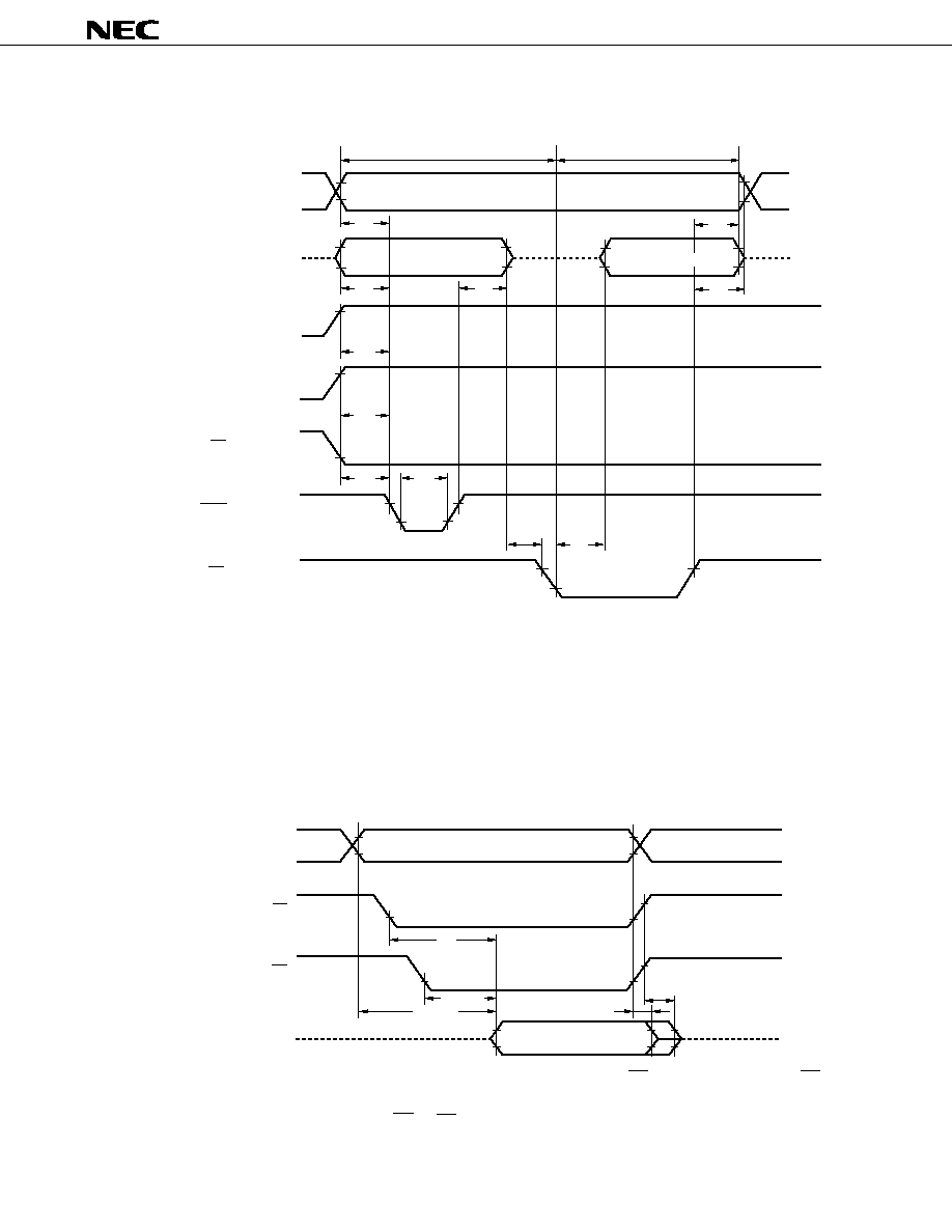
µ
PD78P4916
45
PROM Write Mode Timing (Byte Programming Mode)
Cautions 1. Apply voltage to V
DDP
before applying voltage to V
PP
, and cut off V
DDP
voltage after V
PP
voltage
is cut off.
2. The voltage, including overshoot, applied to V
PP
pin must be kept less than +13.5 V.
3. If a device is inserted or removed while +12.5 V is applied to V
PP
pin, it may be adversely
affected in reliability.
PROM Read Mode Timing
Notes 1. If data need to be read within t
ACC
, the maximum delay time of OE active level input from CE falling
should be t
ACC
≠ t
OE
.
2. t
DF
is the time after either OE or CE first rose to V
IH
.
Programming
Program verify
Hi-Z
Data input
Data output
Hi-Z
Hi-Z
D0 - D7
A0 - A16
V
PP
V
PP
V
DDP
V
DD
+1.5
V
DDP
V
DDP
V
IH
CE
V
IL
V
IH
V
IL
V
IH
V
IL
PGM
OE
t
CES
t
PW
t
VDS
t
VPS
t
DS
t
AS
t
DH
t
AH
t
DF
t
OE
t
OES
Valid address
Hi-Z
Data output
Hi-Z
D0 - D7
A0 - A16
OE
CE
t
CE
t
DF
Note 2
t
OE
Note 1
t
OH
t
ACC
Note 1
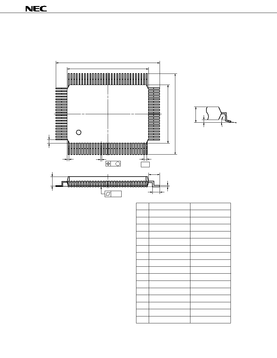
46
µ
PD78P4916
6.
PACKAGE DRAWING
J
N
M
P
80
81
50
100 PIN PLASTIC QFP (14
◊
20)
100
1
31
30
51
G
detail of lead end
S
5∞
±
5∞
C
D
A
B
H
Q
K
L
F
M
I
P100GF-65-3BA1-2
ITEM
MILLIMETERS
INCHES
A
B
C
D
F
G
H
I
J
K
L
23.6±0.4
14.0±0.2
0.6
0.30±0.10
0.15
20.0±0.2
0.929±0.016
0.031
0.024
0.006
0.026 (T.P.)
0.795
NOTE
M
N
0.10
0.15
1.8±0.2
0.65 (T.P.)
0.006
0.031
+0.009
≠0.008
Each lead centerline is located within 0.15
mm (0.006 inch) of its true position (T.P.) at
maximum material condition.
0.012
0.551
0.8±0.2
0.071
P
2.7
0.106
0.693±0.016
17.6±0.4
0.8
+0.008
≠0.009
Q
0.1±0.1
0.004±0.004
S
3.0 MAX.
0.119 MAX.
+0.10
≠0.05
+0.009
≠0.008
+0.004
≠0.005
+0.009
≠0.008
+0.004
≠0.003
0.004
µ
PD78P4916
47
7. RECOMMENDED SOLDERING CONDITIONS
This device should be soldered and mounted under the following conditions.
For details about the recommended conditions, refer to the document "Semiconductor Device Mounting
Technology Manual" (C10535E). For soldering methods and conditions other than those recommended below,
contact your NEC sales representative.
Table 7-1. Surface Mounting Type Soldering Conditions
µ
PD78P4916GF-3BA: 100-pin plastic QFP (14 x 20 mm)
Soldering Method
Soldering Conditions
Symbol
Infrared rays reflow
Peak package's surface temperature: 235 ∞C, Reflow time: 30 seconds or less
IR35-00-2
(at 210 ∞C or higher), Number of reflow processes: 2 or less
<Attention>
(1) Wait for the device temperature to come down to room temperature
after the first reflow before starting the second reflow.
(2) Do not perform flux cleaning of the soldered portion after the first reflow.
VPS
Peak package's surface temperature: 215 ∞C, Reflow time: 40 seconds or less
VP15-00-2
(at 200 ∞C or higher), Number of reflow processes: 2 or less
<Attention>
(1) Wait for the device temperature to come down to room temperature
after the first reflow before starting the second reflow.
(2) Do not perform flux cleaning of the soldered portion after the first reflow.
Wave soldering
Solder temperature: 260 ∞C or below, Flow time: 10 seconds or less, Number of flow
WS60-00-1
process: 1, Preheating temperature; 120 ∞C max. (package surface temperature)
Partial heating
Pin temperature: 300 ∞C or below, Time: 3 seconds or less (per pin row)
--
Caution Do not use different soldering methods together (except for partial heating).
*

48
µ
PD78P4916
APPENDIX A. DEVELOPMENT TOOLS
The following development tools are prepared for system development using the
µ
PD78P4916.
Language Software
RA78K4
Note 1
Assembler package common to the 78K/IV Series
CC78K4
Note 1
C compiler package common to the 78K/IV Series
CC78K4-L
Note 1
C compiler library source file common to the 78K/IV Series
PROM Writing Tool
PG-1500
PROM programmer
PA-78P4916GF
Programmer adapter connected to the PG-1500
PG-1500 Controller
Note 2
Control program for PG-1500
Debugging Tool
IE-784000-R
In-circuit emulator common to the 78K/IV Series
IE-784000-R-BK
Break board common to the 78K/IV Series
IE-784000-R-EM
Emulation board common to the 78K/IV Series
IE-784915-R-EM1
Emulation board for evaluation of the
µ
PD784915 Subseries
IE-78000-R-SV3
Interface adapter when using EWS as a host machine
IE-70000-98-IF-B
Interface adapter when using PC-9800 series (except notebook type) as a host
machine
IE-70000-98N-IF
Interface adapter and cable when using notebook type PC-9800 series as a host
machine
IE-70000-PC-IF-B
Interface adapter when using IBM PC/AT
TM
as a host machine
EP-784915GF-R
Emulation probe common to the
µ
PD784915 subseries
EV-9200GF-100
Conversion socket for 100-pin plastic QFP to mount a device on a target system
SM78K4
Note 3
System emulator for all 78K/IV series devices
ID78K4
Note 3
Integrated debugger for IE-784000-R
DF784915
Note 4
Device file common to the
µ
PD784915 subseries
Real-time OS
RX78K/IV
Note 4
Real-time OS common to the 78K/IV series
MX78K4
Note 2
OS common to the 78K/IV series
*
*

µ
PD78P4916
49
Notes 1. ∑ PC-9800 series (for MS-DOS
TM
) based
∑ IBM PC/AT and compatibles (for PC DOS
TM
, Windows
TM
, MS-DOS, and IBM DOS
TM
) based
∑ HP9000 series 700
TM
(for HP-UX
TM
) based
∑ SPARCstation
TM
(for SunOS
TM
) based
∑ NEWS
TM
(NEWS-OS
TM
) based
2. ∑ PC-9800 series (for MS-DOS) based
∑ IBM PC/AT and its compatibles (for PC DOS, Windows, MS-DOS, and IBM DOS) based
3. ∑ PC-9800 series (for Windows on MS-DOS) based
∑ IBM PC/AT and its compatibles (for PC DOS, Windows, MS-DOS, and IBM DOS) based
∑ HP9000 series 700 (for HP-UX) based
∑ SPARCstation (for SunOS) based
4. ∑ PC-9800 series (for MS-DOS) based
∑ IBM PC/AT and compatibles (for PC DOS, Windows, MS-DOS, and IBM DOS) based
∑ HP9000 series 700 (for HP-UX) based
∑ SPARCstation (for SunOS) based
Remark The RA78K4, CC78K4, SM78K4, and ID78K4 should be used in combination with the DF784915.
*
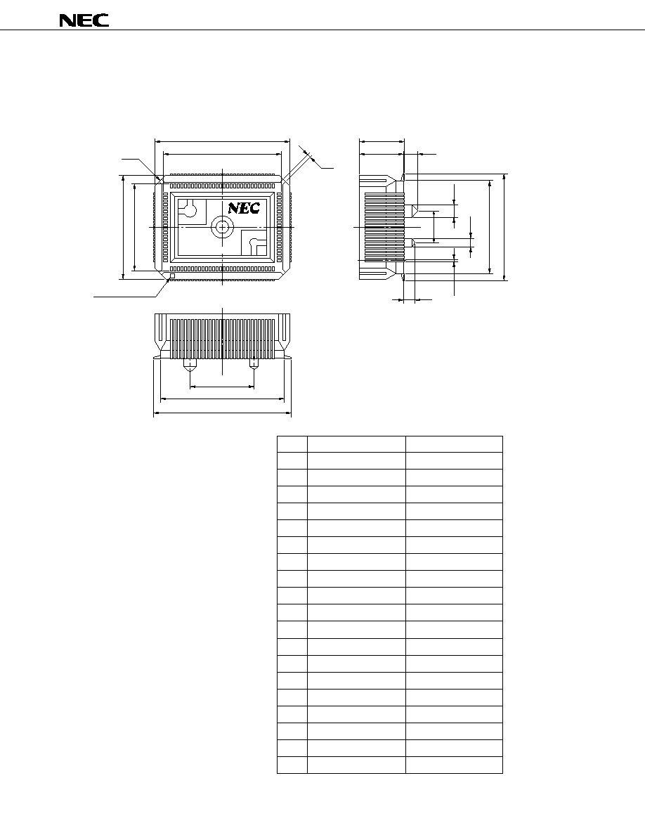
50
µ
PD78P4916
EV-9200GF-100
A
D
E
B
F
1
No.1 pin index
M
N
O
L
K
S
R
Q
I
H
G
P
C
J
EV-9200GF-100-G0
ITEM
MILLIMETERS
INCHES
A
B
C
D
E
F
G
H
I
J
K
L
M
N
O
P
Q
R
S
24.6
21
15
18.6
4-C 2
0.8
12.0
22.6
25.3
6.0
16.6
19.3
8.2
8.0
2.5
2.0
0.35
2.3
1.5
0.969
0.827
0.591
0.732
4-C 0.079
0.031
0.472
0.89
0.996
0.236
0.654
076
0.323
0.315
0.098
0.079
0.014
0.091
0.059
APPENDIX B. SOCKET DRAWING AND RECOMMENDED FOOTPRINT
Figure B-1. EV-9200GF-100 Drawing
(For reference purpose only)
*
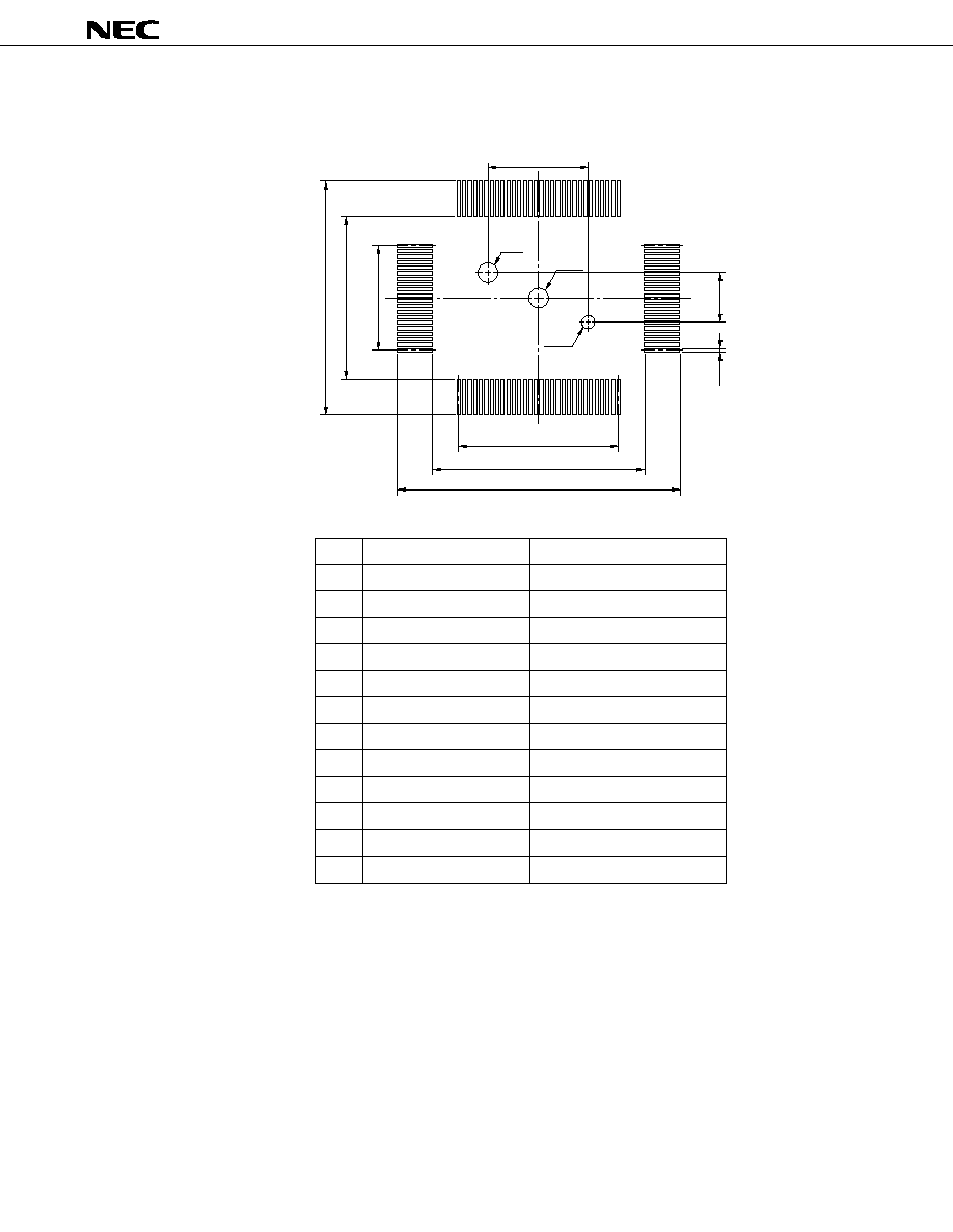
µ
PD78P4916
51
Figure B-2. Recommended EV-9200GF-100 Footprint
(For reference purpose only)
F
H
E
D
A
B
C
I
J
K
L
0.026
◊
1.142=0.742
0.026
◊
0.748=0.486
EV-9200GF-100-P1
ITEM
MILLIMETERS
INCHES
A
B
C
D
E
F
G
H
I
J
K
L
26.3
21.6
15.6
20.3
12±0.05
6±0.05
0.35±0.02
2.36±0.03
2.3
1.57±0.03
1.035
0.85
0.614
0.799
0.472
0.236
0.014
0.093
0.091
0.062
0.65±0.02
◊
29=18.85±0.05
0.65±0.02
◊
19=12.35±0.05
+0.001
≠0.002
+0.002
≠0.002
+0.001
≠0.002
+0.003
≠0.002
+0.003
≠0.002
+0.003
≠0.002
+0.001
≠0.001
+0.001
≠0.002
+0.001
≠0.002
G
Dimensions of mount pad for EV-9200 and that for
target device (QFP) may be different in some parts.
For the recommended mount pad dimensions for
QFP, refer to "SEMICONDUCTOR DEVICE MOUNTING
TECHNOLOGY MANUAL" (C10535E).
Caution
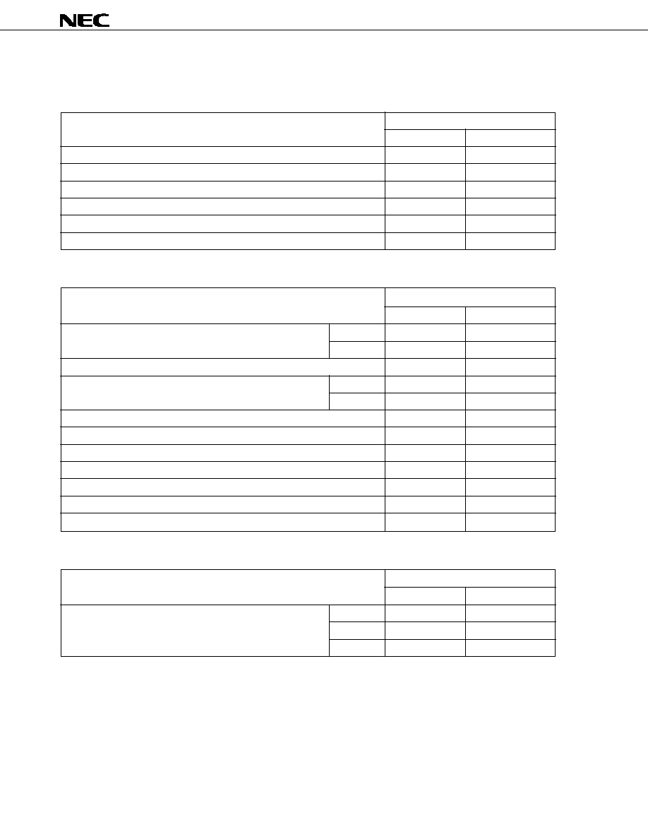
52
µ
PD78P4916
APPENDIX C. RELATED DOCUMENTS
Document related to device
Title
Document No.
Japanese
English
µ
PD784915 Subseries User's Manual ≠ Hardware
U10444J
U10444E
µ
PD784915 Subseries Special Function Register Table
U10976J
--
78K/IV Series User's Manual ≠ Instructions
U10905J
U10905E
78K/IV Series Instruction Table
U10594J
--
78K/IV Series Instruction Set
U10595J
--
78K/IV Series Application Note ≠ Software Basics
U10095J
--
Development tool documents (User's Manual)
Title
Document No.
Japanese
English
RA78K Series Assembler Package
Language
EEU-809
EEU-1399
Operation
EEU-815
EEU-1404
RA78K Series Structured Assembler Preprocessor
EEU-817
EEU-1402
CC78K Series C Compiler
Language
EEU-656
EEU-1280
Operation
EEU-655
EEU-1284
CC78K Series Library Source File
EEU-777
--
PG-1500 PROM Programmer
EEU-651
EEU-1335
PG-1500 Controller PC-9800 series ≠ MS-DOS base
EEU-704
EEU-1291
PG-1500 Controller IBM PC series ≠ PC DOS base
EEU-5008
U10540E
IE-784000-R
EEU-5004
EEU-1534
IE-784915-R-EM1 EP-784915GF-R
U10931J
--
ID78K4 Integrated Debugger ≠ Reference
U10440J
IEU-1412
Embedded-software documents (User's Manual)
Title
Document No.
Japanese
English
RX78K/IV Series Real-time OS
Basics
U10604J
--
Installation
U10603J
--
Debugger
U10364J
--
Caution The contents of the documents listed above are subject to change without prior notice to users.
Be sure to use the latest edition when starting design.
*
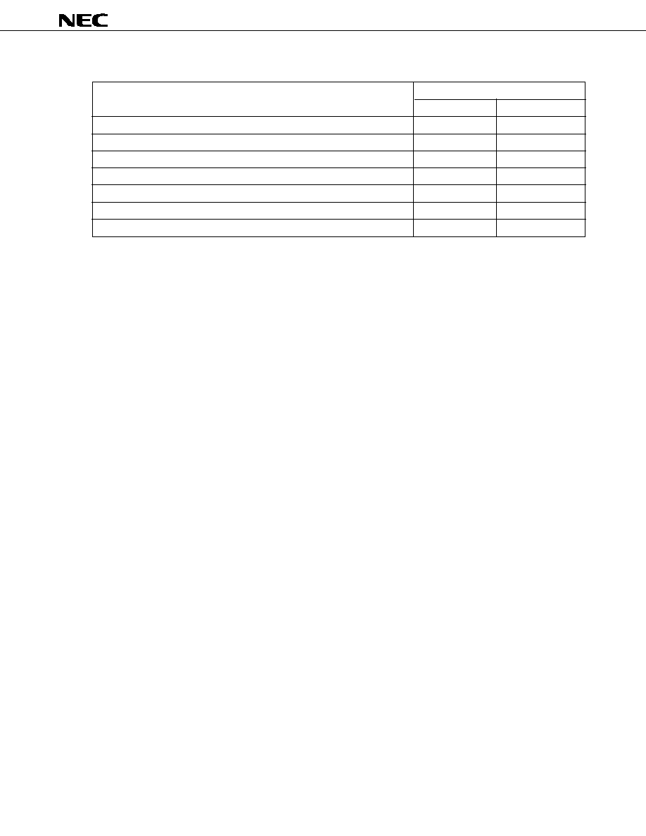
µ
PD78P4916
53
Other documents
Title
Document No.
Japanese
English
Semiconductor Device Package Manual
IEI-635
IEI-1213
Semiconductor Device Mounting Technology Manual
C10535J
C10535E
Quality Grades on NEC Semiconductor Devices
IEI-620
IEI-1209
NEC Semiconductor Device Reliability/Quality Control System
IEM-5068
--
Electrostatic Discharge (ESD) Test
MEM-539
--
Guide to Quality Assurance for Semiconductor Devices
MEI-603
MEI-1202
Microcontroller-Related Product Guide - Third Party Products
MEI-604
--
Caution The contents of the documents listed above are subject to change without prior notice to users.
Be sure to use the latest edition when starting design.
*

54
µ
PD78P4916
[MEMO]
µ
PD78P4916
55
NOTES FOR CMOS DEVICES
1
PRECAUTION AGAINST ESD FOR SEMICONDUCTORS
Note: Strong electric field, when exposed to a MOS device, can cause destruction of
the gate oxide and ultimately degrade the device operation. Steps must be
taken to stop generation of static electricity as much as possible, and quickly
dissipate it once, when it has occurred. Environmental control must be
adequate. When it is dry, humidifier should be used. It is recommended to avoid
using insulators that easily build static electricity. Semiconductor devices
must be stored and transported in an anti-static container, static shielding bag
or conductive material. All test and measurement tools including work bench
and floor should be grounded. The operator should be grounded using wrist
strap. Semiconductor devices must not be touched with bare hands. Similar
precautions need to be taken for PW boards with semiconductor devices on it.
2
HANDLING OF UNUSED INPUT PINS FOR CMOS
Note: No connection for CMOS device inputs can be cause of malfunction. If no
connection is provided to the input pins, it is possible that an internal input level
may be generated due to noise, etc., hence causing malfunction. CMOS devices
behave differently than Bipolar or NMOS devices. Input levels of CMOS devices
must be fixed high or low by using a pull-up or pull-down circuitry. Each unused
pin should be connected to V
DD
or GND with a resistor, if it is considered to have
a possibility of being an output pin. All handling related to the unused pins must
be judged device by device and related specifications governing the devices.
3
STATUS BEFORE INITIALIZATION OF MOS DEVICES
Note: Power-on does not necessarily define initial status of MOS device. Production
process of MOS does not define the initial operation status of the device.
Immediately after the power source is turned ON, the devices with reset function
have not yet been initialized. Hence, power-on does not guarantee out-pin
levels, I/O settings or contents of registers. Device is not initialized until the
reset signal is received. Reset operation must be executed immediately after
power-on for devices having reset function.

µ
PD78P4916
No part of this document may be copied or reproduced in any form or by any means without the prior written
consent of NEC Corporation. NEC Corporation assumes no responsibility for any errors which may appear in this
document.
NEC Corporation does not assume any liability for infringement of patents, copyrights or other intellectual
property rights of third parties by or arising from use of a device described herein or any other liability arising
from use of such device. No license, either express, implied or otherwise, is granted under any patents,
copyrights or other intellectual property rights of NEC Corporation or others.
While NEC Corporation has been making continuous effort to enhance the reliability of its semiconductor devices,
the possibility of defects cannot be eliminated entirely. To minimize risks of damage or injury to persons or
property arising from a defect in an NEC semiconductor device, customer must incorporate sufficient safety
measures in its design, such as redundancy, fire-containment, and anti-failure features.
NEC devices are classified into the following three quality grades:
"Standard", "Special", and "Specific". The Specific quality grade applies only to devices developed based on
a customer designated "quality assurance program" for a specific application. The recommended applications
of a device depend on its quality grade, as indicated below. Customers must check the quality grade of each
device before using it in a particular application.
Standard: Computers, office equipment, communications equipment, test and measurement equipment,
audio and visual equipment, home electronic appliances, machine tools, personal electronic
equipment and industrial robots
Special:
Transportation equipment (automobiles, trains, ships, etc.), traffic control systems, anti-disaster
systems, anti-crime systems, safety equipment and medical equipment (not specifically designed
for life support)
Specific: Aircrafts, aerospace equipment, submersible repeaters, nuclear reactor control systems, life
support systems or medical equipment for life support, etc.
The quality grade of NEC devices in "Standard" unless otherwise specified in NEC's Data Sheets or Data Books.
If customers intend to use NEC devices for applications other than those specified for Standard quality grade,
they should contact NEC Sales Representative in advance.
Anti-radioactive design is not implemented in this product.
M4 94.11
The application circuits and their parameters are for reference only and are not intended for use in actual design-in's.
FIP is a trademark of NEC Corporation.
MS-DOS and Windows are trademarks of Microsoft Corporation.
IBM DOS, PC/AT, and PC DOS are trademarks of International Business Machines Corporation.
HP9000 Series 700 and HP-UX are trademarks of Hewlett-Packard Company.
SPARCstation is a trademark of SPARC International, Inc.
SunOS is a trademark of Sun Microsystems, Inc.
NEWS and NEWS-OS are trademarks of Sony Corporation.
The related documents indicated in this publication may include preliminary versions. However, preliminary
versions are not marked as such.
The export of this product from Japan is regulated by the Japanese government. To export this product may be prohibited
without governmental license, the need for which must be judged by the customer. The export or re-export of this product
from a country other than Japan may also be prohibited without a license from that country. Please call an NEC sales
representative.