 | –≠–Ľ–Ķ–ļ—ā—Ä–ĺ–Ĺ–Ĺ—č–Ļ –ļ–ĺ–ľ–Ņ–ĺ–Ĺ–Ķ–Ĺ—ā: UPD8891 | –°–ļ–į—á–į—ā—Ć:  PDF PDF  ZIP ZIP |
Document Outline
- COVER
- DESCRIPTION
- FEATURES
- ORDERING INFORMATION
- BLOCK DIAGRAM
- PIN CONFIGURATION (Top View)
- PHOTOCELL STRUCTURE DIAGRAM
- PHOTOCELL ARRAY STRUCTURE DIAGRAM 1 (Line Spacing)
- PHOTOCELL ARRAY STRUCTURE DIAGRAM 2 (The Relation of the Photocell Array)
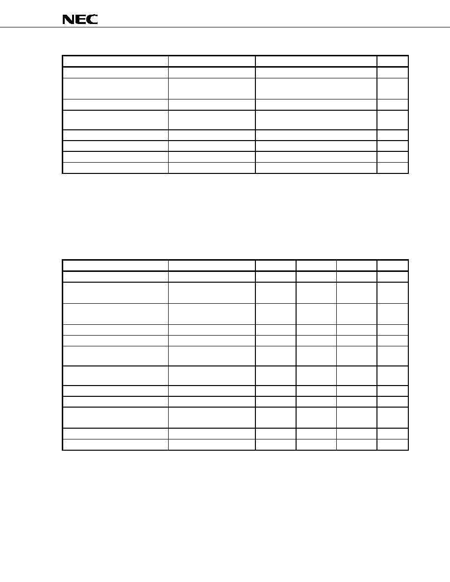
- ABSOLUTE MAXIMUM RATINGS (TA = +25 degrees)
- RECOMMENDED OPERATING CONDITIONS (TA = +25 degrees)
- ELECTRICAL CHARACTERISTICS
- INPUT PIN CAPACITANCE (TA = +25 degrees, VOD = 12 V)
- 300/600/1200 MODE
- TIMING CHART 1-1 (1200 dpi, for each color)
- TIMING CHART 1-2 (600 dpi, even pixel, for each color)
- TIMING CHART 1-3 (600 dpi, odd pixel, for each color)
- TIMING CHART 1-4 (300 dpi, for each color)
- TIMING CHART 2-1 (1200 dpi, bit clamp mode, for each color)
- TIMING CHART 2-2 (1200 dpi, line clamp mode, for each color)
- TIMING CHART 2-3 (600 dpi, even pixel, bit clamp mode, for each color)
- TIMING CHART 2-4 (600 dpi, even pixel, line clamp mode, for each color)
- TIMING CHART 2-5 (600 dpi, odd pixel, bit clamp mode, for each color)
- TIMING CHART 2-6 (600 dpi, odd pixel, line clamp mode, for each color)
- TIMING CHART 2-7 (300 dpi, bit clamp mode, for each color)
- TIMING CHART 2-8 (300 dpi, line clamp mode, for each color)
- Ģˇ
- Ģˇ
- Ģˇ
- Ģˇ
- Ģˇ
- DEFINITIONS OF CHARACTERISTIC ITEMS
- STANDARD CHARACTERISTIC CURVES (Reference Value)
- APPLICATION CIRCUIT EXAMPLE
- PACKAGE DRAWING
- RECOMMENDED SOLDERING CONDITIONS

MOS INTEGRATED CIRCUIT
Ķ
Ķ
Ķ
Ķ
PD8891
(5340
◊
◊
◊
◊ 5340) PIXELS ◊◊◊◊ 3 + 2670 PIXELS ◊◊◊◊ 3 COLOR CCD LINEAR IMAGE SENSOR
DATA SHEET
Document No. S16039EJ2V0DS00 (2nd edition)
Date Published March 2003 NS CP (K)
Printed in Japan
The information in this document is subject to change without notice. Before using this document, please
confirm that this is the latest version.
Not all products and/or types are available in every country. Please check with an NEC Electronics
sales representative for availability and additional information.
2002
DESCRIPTION
The
Ķ
PD8891 is a color CCD (Charge Coupled Device) linear image sensor which changes optical images to
electrical signal and has the function of color separation.
The
Ķ
PD8891 has 3 rows of (5340+5340) staggered pixels, and each row has a dual-sided readout type of charge
transfer register, and has 3 rows of 2670 pixels, and each row has a single-sided readout type of charge transfer
register. And it has reset feed-through level clamp circuits and voltage amplifiers. Therefore, it is suitable for 1200
dpi/A4 color image scanners, color facsimiles and so on.
FEATURES
∑ Valid photocell
: (5340+5340) pixels
◊ 3 + 2670 pixels ◊ 3
∑ Photocell pitch
: 5.25
Ķ
m (1200 dpi), 10.5
Ķ
m (300 dpi)
∑ Photocell size
: 5.25
◊ 5.25
Ķ
m
2
(1200 dpi), 10.5
◊ 8
Ķ
m
2
(300 dpi)
∑ Line spacing
: [1200 dpi sensor]
52.5
Ķ
m (10 lines) Red line - Green line, Green line - Blue line
10.5
Ķm (2 lines) Odd line ≠ Even line (for each color)
[300 dpi sensor]
42
Ķ
m (4 lines) Red line - Green line, Green line - Blue line
∑ Color filter
: Primary colors (red, green and blue), pigment filter (with light resistance 10
7
lx∑hour)
∑ Resolution
: 48 dot/mm A4 (210
◊ 297 mm) size (shorter side)
:
1200 dpi US letter (8.5"
◊ 11") size (shorter side)
∑ Drive clock level : CMOS output under 5 V operation
∑ Data rate
: 5 MHz Max.
∑ Power supply
: +12 V
∑ On-chip circuits : Reset feed-through level clamp circuits
::
Voltage amplifiers
ORDERING INFORMATION
Part Number
Package
Ķ
PD8891CY
CCD linear image sensor 22-pin plastic DIP (10.16 mm (400))
Data Sheet S16039EJ2V0DS
2
Ķ
Ķ
Ķ
Ķ
PD8891
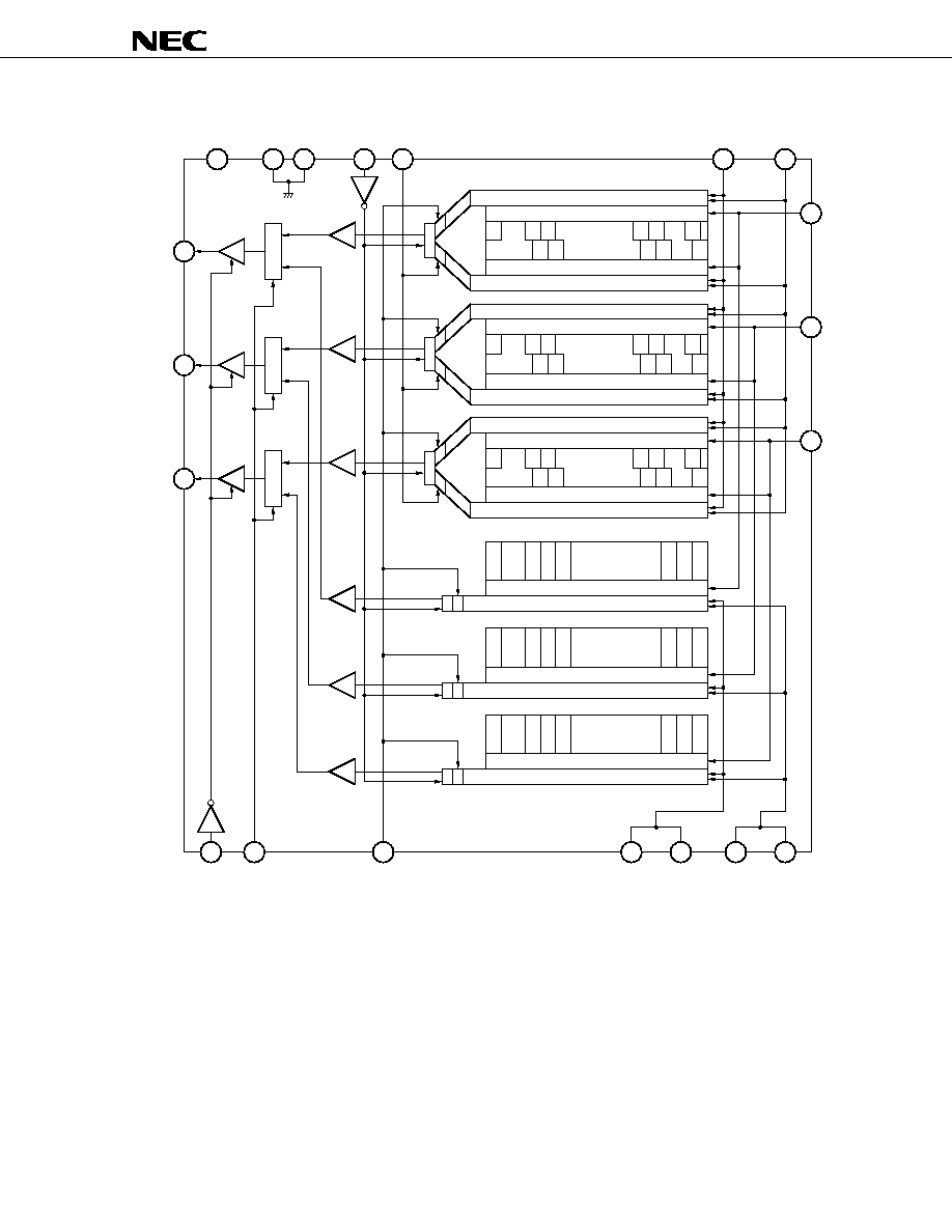
BLOCK DIAGRAM
22
20
1
11
7
8
16
15
5
17
TG1
(Blue)
TG2
(Green)
TG3
(Red)
1L
2-1200
1-1200
2-300
1-300
14
13
2-300
1-300
GND GND
V
OD
V
OUT
1
(Blue)
21
V
OUT
2
(Green)
2
12
10
9
V
OUT
3
(Red)
CLB
19
SEL
Photocell
(Blue)
CCD analog shift register
CCD analog shift register
Transfer gate
Transfer gate
∑ ∑ ∑ ∑
∑∑∑
D154
D156
S10680
S2
D162
D47
D155
S10679
S1
D161
D153
∑∑∑
D162
D161
∑∑∑
D162
D161
∑ ∑ ∑ ∑
D154
D156
S10680
S2
D47
D155
S10679
S1
D153
∑ ∑ ∑ ∑
D154
D156
S10680
S2
D47
D155
S10679
S1
D153
Photocell
(Green)
CCD analog shift register
CCD analog shift register
Transfer gate
Transfer gate
Photocell
(Red)
CCD analog shift register
CCD analog shift register
Transfer gate
Transfer gate
4
RB
3
2L
Photocell
(Blue)
CCD analog shift register
Transfer gate
∑ ∑ ∑ ∑
D40
S2670
D13
D39
S1
S2
D41
Photocell
(Green)
CCD analog shift register
Transfer gate
∑ ∑ ∑ ∑
D13
D39
S1
S2
Photocell
(Red)
CCD analog shift register
Transfer gate
∑ ∑ ∑ ∑
D13
D39
S1
S2
D40
S2670
D41
D40
S2670
D41
Data Sheet S16039EJ2V0DS
3
Ķ
Ķ
Ķ
Ķ
PD8891
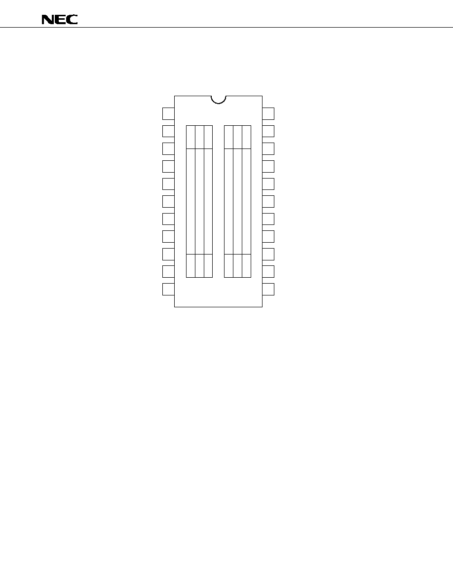
PIN CONFIGURATION (Top View)
CCD linear image sensor 22-pin plastic DIP (10.16 mm (400))
∑
Ķ
PD8891CY
NC
No connection
V
OUT
2
Output signal 2 (Green)
V
OUT
1
Output signal 1 (Blue)
2670
2670
2670
Red
Green
Blue
1
1
1
TG1
Transfer gate clock 1 (for Blue)
Output drain voltage
V
OD
SEL
300/1200 dpi select input
1-300
Shift register clock 1
(for 300 dpi)
2-300
Shift register clock 2
(for 300 dpi)
1-300
Shift register clock 1
(for 300 dpi)
2-300
Shift register clock 2
(for 300 dpi)
Last stage shift register clock 1
1L
22
21
20
19
18
17
16
15
14
13
12
1
2
3
4
5
6
7
8
9
10
11
GND
Ground
V
OUT
3
Output signal 3 (Red)
10680
10680
10680
Red
Green
Blue
1
1
1
TG3
Transfer gate clock 3 (for Red)
TG2
Transfer gate clock 2 (for Green)
Shift register clock 2
(for 1200 dpi)
2-1200
Shift register clock 1
(for 1200 dpi)
1-1200
GND
Ground
Reset gate clock
RB
Last stage shift register clock 2
2L
Reset feed-through level
level clamp clock
CLB
No connection
NC
Caution Connect the No connection pins (NC) to GND.
Data Sheet S16039EJ2V0DS
4
Ķ
Ķ
Ķ
Ķ
PD8891
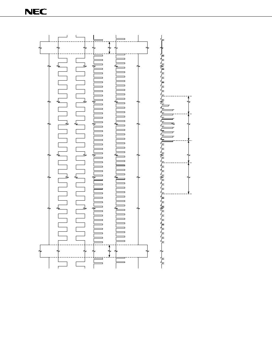
PHOTOCELL STRUCTURE DIAGRAM
1200 dpi sensor
300 dpi sensor
5.25 m
Ķ
2.75 m
Ķ
Ķ
m
2.5
Channel stopper
Aluminium shield
8.0 m
Ķ
8.0 m
Ķ
Ķ
m
2.5
Channel stopper
Aluminium shield
PHOTOCELL ARRAY STRUCTURE DIAGRAM 1 (Line Spacing)
Blue photocell array
1200 dpi sensor
300 dpi sensor
Blue photocell array
Green photocell array
Green photocell array
5.25
Ķ
m
8 lines
(42
Ķ
m)
2 lines
(10.5
Ķ
m)
5.25
Ķ
m
5.25
Ķ
m
5.25
Ķ
m
5.25
Ķ
m
5.25
Ķ
m
Red photocell array
Red photocell array
8 lines
(42
Ķ
m)
10 lines
(52.5
Ķ
m)
42
Ķ
m
5.25
Ķ
m
10 lines
(52.5
Ķ
m)
2 lines
(10.5
Ķ
m)
5.25
Ķ
m
5.25
Ķ
m
5.25
Ķ
m
Blue photocell array
10.5
Ķ
m
Green photocell array
10.5
Ķ
m
Red photocell array
10.5
Ķ
m
4 lines
(42
Ķ
m)
4 lines
(42
Ķ
m)
Data Sheet S16039EJ2V0DS
5
Ķ
Ķ
Ķ
Ķ
PD8891
PHOTOCELL ARRAY STRUCTURE DIAGRAM 2 (The Relation of the Photocell Array)
1-45
47-145
147 149 151 153 155 157
-
2-46
48-146
148 150 152 154 156 158
-
1-12
12 pixels
300 dpi
1200 dpi
13-37
25 pixels
2 pixels
2670 pixels
38, 39
2709
40
2710,
2711
2 pixels
46 pixels
100 pixels
8 pixels
10680 pixels
8 pixels
Dummy
Optical black
Invalid photocell
Valid photocell
Invalid photocell
-
10832 10834 10836-10842
10831 10833
10835-10841
Data Sheet S16039EJ2V0DS
6
Ķ
Ķ
Ķ
Ķ
PD8891
ABSOLUTE MAXIMUM RATINGS (T
A
=
+
+
+
+25įįįįC)
Parameter
Symbol
Ratings
Unit
Output drain voltage
V
OD
-0.3 to +15
V
Shift register clock voltage
V
1-300
, V
1-1200
, V
1L
,
-0.3 to +8
V
V
2-300
, V
2-1200
, V
2L
Reset gate clock voltage
V
RB
-0.3 to +8
V
Reset feed-through level clamp
clock voltage
V
CLB
-0.3 to +8
V
300/1200 dpi select signal voltage
V
SEL
-0.3 to +8
V
Transfer gate clock voltage
V
TG1
to V
TG3
-0.3 to +8
V
Operating ambient temperature
Note
T
A
0 to
+60
įC
Storage temperature
T
stg
-40 to +70
įC
Note Use at the condition without dew condensation.
Caution Product quality may suffer if the absolute maximum rating is exceeded even momentarily for any
parameter. That is, the absolute maximum ratings are rated values at which the product is on the
verge of suffering physical damage, and therefore the product must be used under conditions
that ensure that the absolute maximum ratings are not exceeded.
RECOMMENDED OPERATING CONDITIONS (T
A
=
+
+
+
+25įįįįC)
Parameter
Symbol
Min.
Typ.
Max.
Unit
Output drain voltage
V
OD
11.4
12.0
12.6
V
Shift register clock high level
V
1-300H
, V
1-1200H
, V
1LH
,
4.75
5.0
5.25
V
V
2-300H
, V
2-1200H
, V
2LH
Shift register clock low level
V
1-300L
, V
1-1200L
, V
1LL
,
-0.3
0
+0.25
V
V
2-300L
, V
2-1200L
, V
2LL
Reset gate clock high level
V
RBH
4.5
5.0
5.5
V
Reset gate clock low level
V
RBL
-0.3
0
+0.5
V
Reset feed-through level clamp clock
high level
V
CLBH
4.5
5.0
5.5
V
Reset feed-through level clamp clock
low level
V
CLBL
-0.3
0
+0.5
V
300/1200 dpi select signal high level
V
SELH
4.5
5.0
5.5
V
300/1200 dpi select signal low level
V
SELL
-0.3
0
+0.5
V
Transfer gate clock high level
V
TG1H
to V
TG3H
4.75
V
1-300H
,
V
1-1200H
Note
V
1-300H
,
V
1-1200H
Note
V
Transfer gate clock low level
V
TG1L
to V
TG3L
-0.3
0
+0.15
V
Data rate
f
RB
-
2.0
5.0
MHz
Note
When Transfer gate clock high level (V
TG1H
to V
TG3H
) is higher than shift register clock high level (V
1-300H
,
V
1-1200H
), image lag can increase.
Data Sheet S16039EJ2V0DS
7
Ķ
Ķ
Ķ
Ķ
PD8891
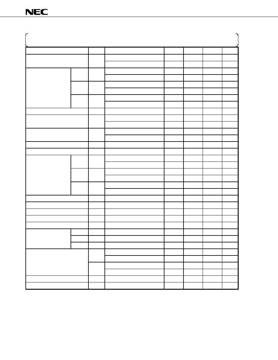
ELECTRICAL CHARACTERISTICS
T
A
=
+25įC, V
OD
= 12 V, data rate (f
RB
) = 2 MHz, storage time = 11.0 ms, input signal clock = 5 V
p-p
,
light source : 3200 K halogen lamp
+ C-500S (infrared cut filter, t = 1 mm) + HA-50 (heat absorbing filter, t = 3 mm)
Parameter
Symbol
Test Conditions
Min.
Typ.
Max.
Unit
Saturation voltage
V
sat
300 dpi
2.5
2.7
-
V
1200 dpi
2.0
2.4
-
V
Saturation exposure
Red
SER
300 dpi
-
0.167
-
lx∑s
1200 dpi
-
0.445
-
lx∑s
Green
SEG
300 dpi
-
0.176
-
lx∑s
1200 dpi
-
0.470
-
lx∑s
Blue
SEB
300 dpi
-
0.274
-
lx∑s
1200 dpi
-
0.732
-
lx∑s
Photo response non-uniformity
PRNU
V
OUT
= 1.0 V
-
6
20
%
Average dark signal
ADS
Light shielding
300 dpi
-
0.4
4.0
mV
Light shielding
1200 dpi
-
0.2
2.0
mV
Dark signal non-uniformity
DSNU
Light shielding
300 dpi
-
4.0
12.0
mV
Light shielding
1200 dpi
-
2.0
6.0
mV
Power consumption
P
W
-
300
480
mW
Output impedance
Z
O
-
0.4
1.0
k
Response
Red
R
R
300 dpi
11.32
16.17
21.02
V/lx∑s
1200 dpi
3.77
5.39
7.01
V/lx∑s
Green
R
G
300 dpi
10.73
15.33
19.93
V/lx∑s
1200 dpi
3.58
5.11
6.64
V/lx∑s
Blue
R
B
300 dpi
6.89
9.84
12.79
V/lx∑s
1200 dpi
2.30
3.28
4.26
V/lx∑s
Offset level
Note 1
V
OS
4.5
6.0
7.5
V
Image lag
IL
V
OUT
= 1.0 V
-
3.0
7.0
%
Output fall delay time
Note 2
t
d
V
OUT
= 1.0 V
-
25
-
ns
Total transfer efficiency
TTE
V
OUT
= 1.0 V, data rate = 5 MHz
92
98
-
%
Register imbalance
RI
V
OUT
= 1.0 V
(1200 dpi)
-
1.0
4.0
%
Response peak
Red
-
630
-
nm
Green
-
540
-
nm
Blue
-
460
-
nm
Dynamic range
DR1
V
sat
/DSNU
300 dpi
-
675
-
times
V
sat
/DSNU
1200 dpi
-
1200
-
times
DR2
V
sat
/
CDS
300 dpi
-
2700
-
times
V
sat
/
CDS
1200 dpi
-
2400
-
times
Reset feed-through noise
Note 1
RFTN
Light shielding
-2000
-500
+1000
mV
Random noise (CDS)
CDS
Light shielding
-
1.0
-
mV
Notes 1. Refer to TIMING CHART 2
-
-
-
-1 to 2----8.
2. When the fall time of
1L or
2L (t1', t2') is the Typ. value (refer to TIMING CHART 2
-
-
-
-1 to 2----8).
Data Sheet S16039EJ2V0DS
8
Ķ
Ķ
Ķ
Ķ
PD8891
INPUT PIN CAPACITANCE (T
A
=
+
+
+
+25įįįįC, V
OD
= 12 V)
Parameter
Symbol
Pin name
Pin No.
Min.
Typ.
Max.
Unit
Shift register clock pin capacitance 1
C
1-300
1-300
13
-
250
-
pF
15
-
250
-
pF
C
1-1200
1-1200
8
-
850
-
pF
Shift register clock pin capacitance 2
C
2-300
2-300
14
-
300
-
pF
16
-
300
-
pF
C
2-1200
2-1200
7
-
850
-
pF
Last stage sift reset gate clock pin capacitance 1
C
1L
1L
17
-
15
-
pF
Last stage sift reset gate clock pin capacitance 2
C
2L
2L
3
-
15
-
pF
Reset gate clock pin capacitance
C
RB
RB
4
-
15
-
pF
Reset feed-through level clamp clock pin capacitance
C
CLB
CLB
5
-
15
-
pF
300/1200 dpi select signal pin capacitance
C
SEL
SEL
19
-
15
-
pF
Transfer gate clock pin capacitance
C
TG
TG1
12
-
200
-
pF
TG2
10
-
200
-
pF
TG3
9
-
200
-
pF
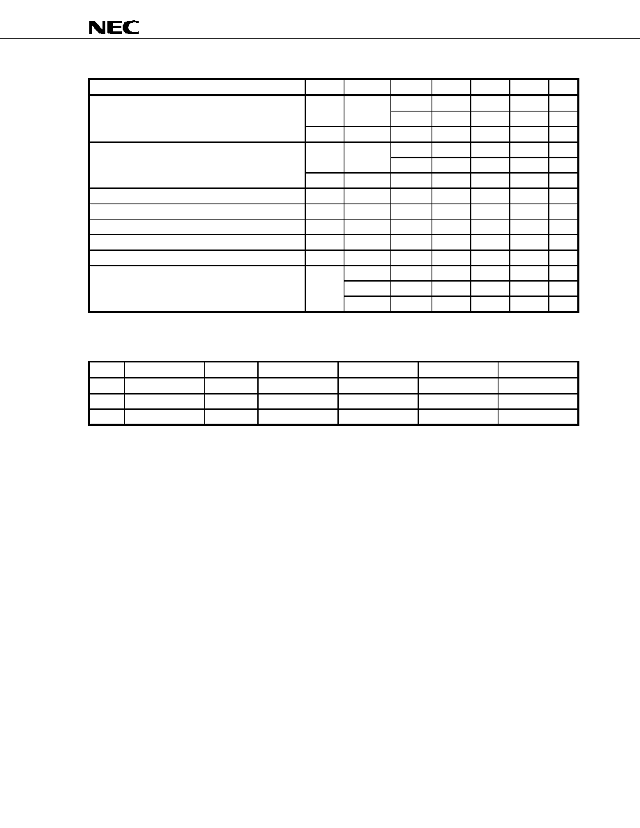
300/600/1200 MODE
Mode
Description
SEL
300 dpi data
1-300, 2-300
1200 dpi data
1-1200, 2-1200
1
300 dpi only
High
Use
Clocked
Flush
Note 2
Clocked
2
600 dpi only
Note 1
Low
Flush
Note 2
Clocked
Use 1 line
Clocked
3
1200 dpi only
Low
Flush
Note 2
Clocked
Use
Clocked
Notes 1. For 600 dpi mode, the reset pulse is extended to allow second line's charge to dump immediately to DC
level.
2. Flush means that data is continuously sunk via reset gate.
D
a
ta S
h
e
e
t S
1
6
039E
J2V
0
D
S
9
Ķ
Ķ
Ķ
Ķ
PD8891
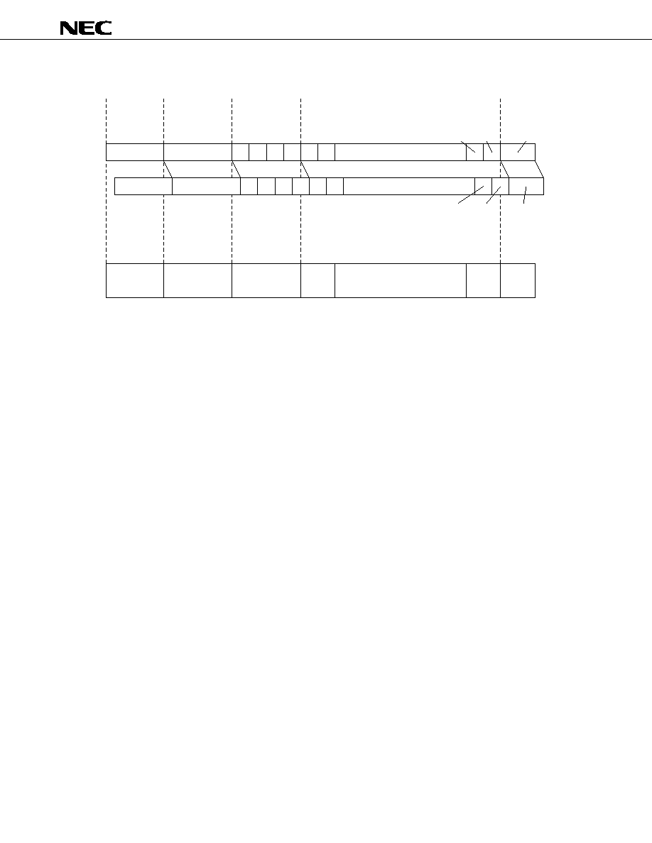
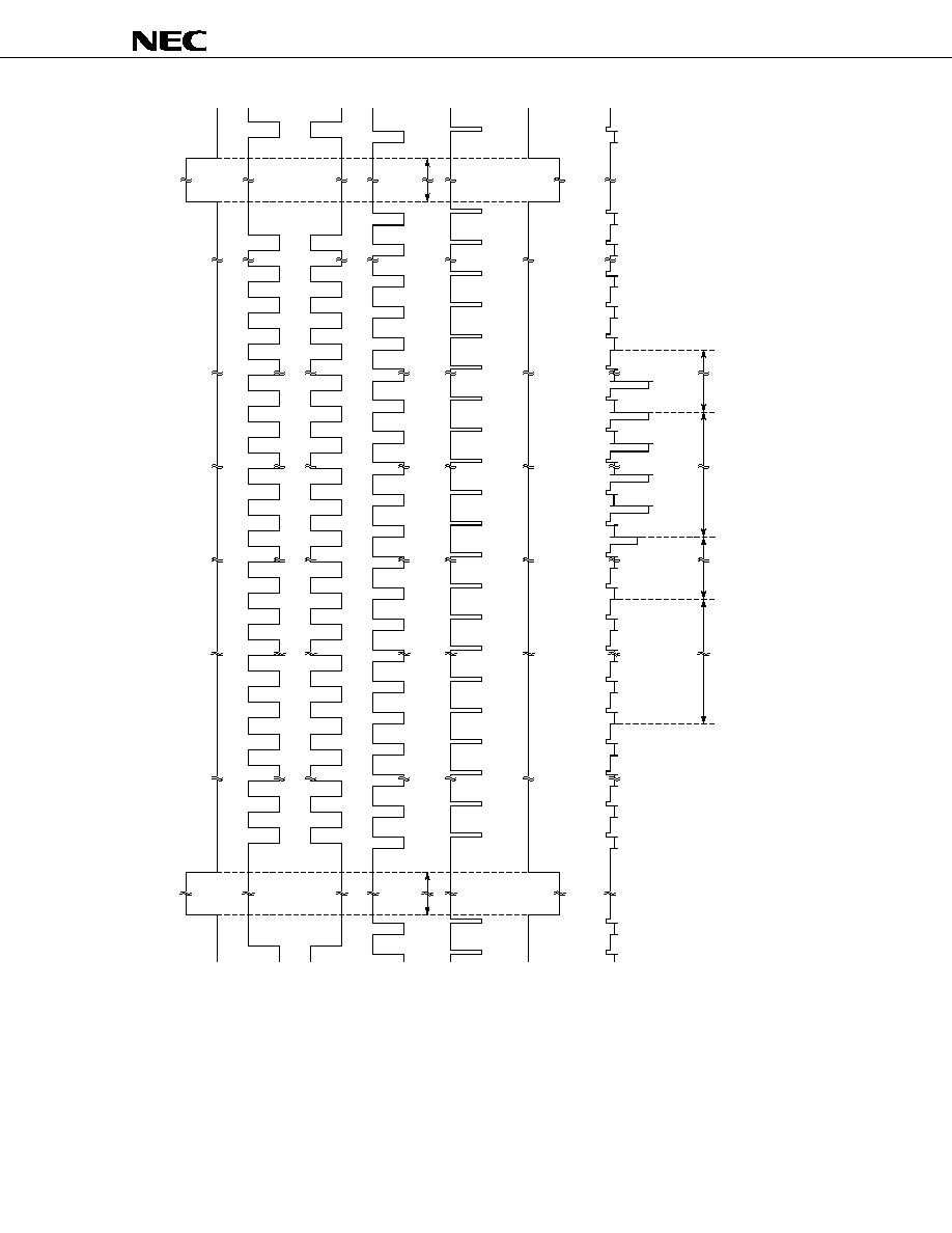
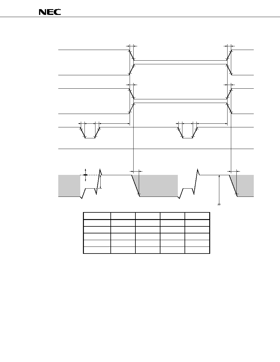
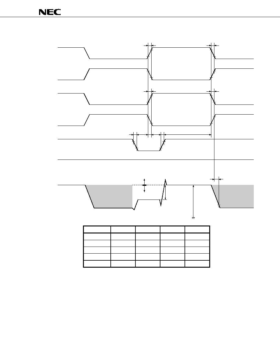
TIMING CHART 1
-
-
-
-1 (1200 dpi, for each color)
1
2
3
4
5
6
45
46
47
146
147
154
155
10834
10835
10842
10843
V
OUT
1 to V
OUT
3
RB
CLB (Bit clamp mode)
CLB (Line clamp mode)
Optical black
(100 pixels)
1L
2L
1-1200,
2-1200,
TG1 to
TG3
Invalid photocell
(8 pixels)
Valid photocell
(10680 pixels)
Invalid photocell
(8 pixels)
Note
Note
Note Set the
RB pulse and
CLB pulse (bit clamp mode) to high level during the
TG1 to
TG3 pulse.
And set the
RB pulse to high level while the
CLB pulse is low level at line clamp mode.
Remark Inverse pulse of the
TG1 to
TG3 can be used as
CLB at line clamp mode.
D
a
ta S
h
e
e
t S
1
6
039E
J2V
0
D
S
10
Ķ
Ķ
Ķ
Ķ
PD8891
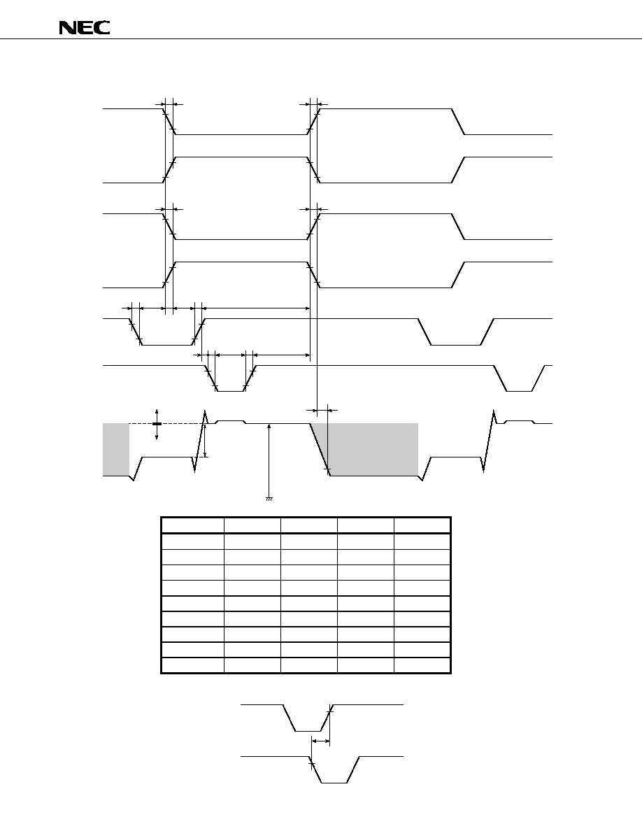
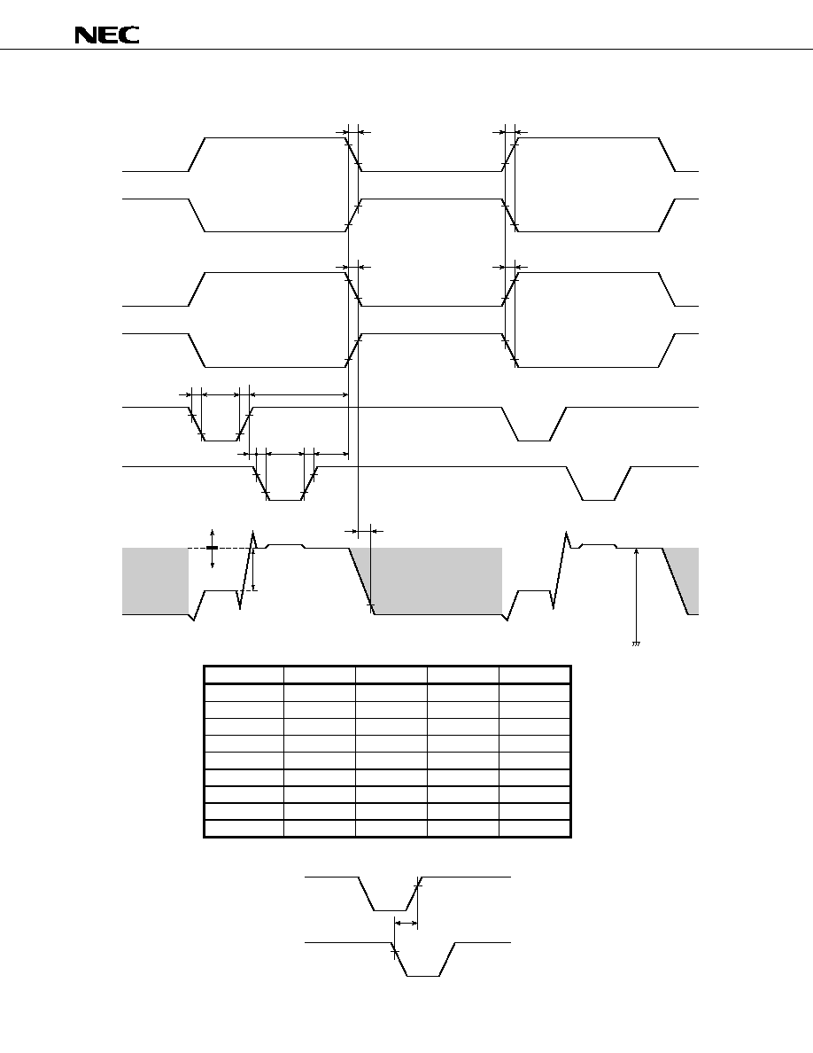
TIMING CHART 1
-
-
-
-2 (600 dpi, even pixel, for each color)
2
4
44
46
48
50
144
146
148
154
156
158
10832
10834
10836
10842
Optical black
(50 pixels)
Invalid photocell
(4 pixels)
Valid photocell
(5340 pixels)
Invalid photocell
(4 pixels)
Note
Note
V
OUT
1 to V
OUT
3
RB
CLB (Bit clamp mode)
CLB (Line clamp mode)
1L
2L
1-1200,
2-1200,
TG1 to
TG3
Note Set the
RB pulse and
CLB pulse (bit clamp mode) to high level during the
TG1 to
TG3 pulse.
And set the
RB pulse to high level while the
CLB pulse is low level at line clamp mode.
Remark Inverse pulse of the
TG1 to
TG3 can be used as
CLB at line clamp mode.
D
a
ta S
h
e
e
t S
1
6
039E
J2V
0
D
S
11
Ķ
Ķ
Ķ
Ķ
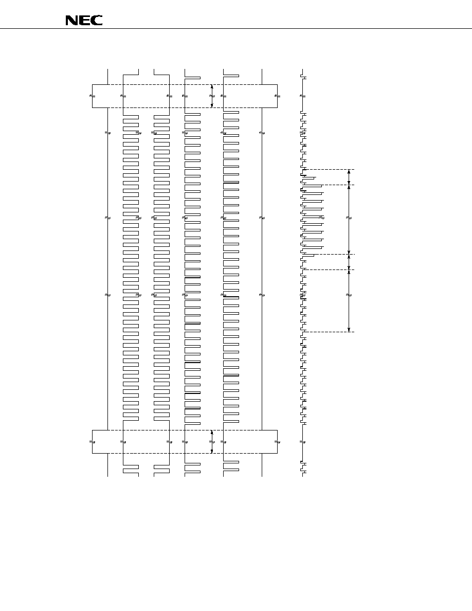
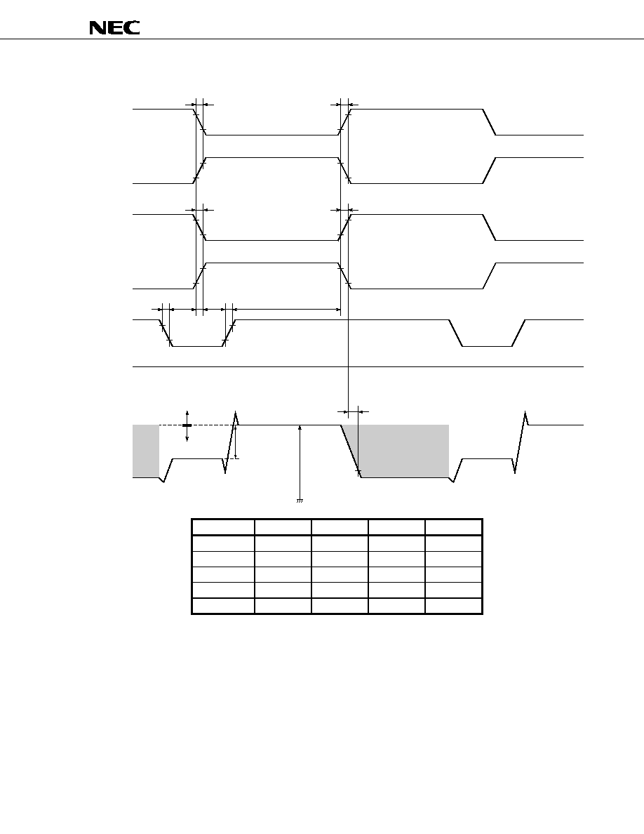
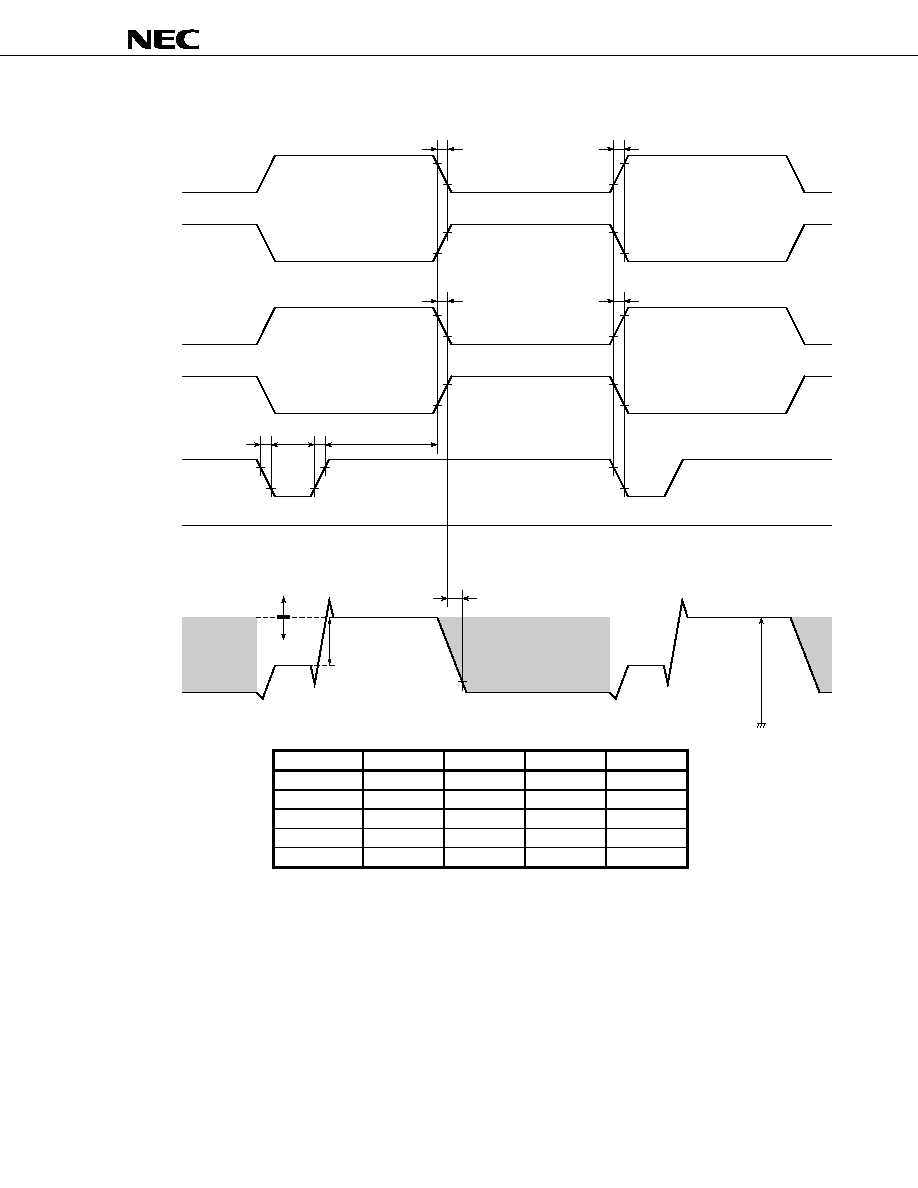
PD8891
TIMING CHART 1
-
-
-
-3 (600 dpi, odd pixel, for each color)
1
3
43
45
47
49
143
145
147
153
155
157
10831
10833
10835
10841
Optical black
(50 pixels)
Invalid photocell
(4 pixels)
Valid photocell
(5340 pixels)
Invalid photocell
(4 pixels)
Note
Note
V
OUT
1 to V
OUT
3
RB
CLB (Bit clamp mode)
CLB (Line clamp mode)
1L
2L
1-1200,
2-1200,
TG1 to
TG3
Note Set the
RB pulse and
CLB pulse (bit clamp mode) to high level during the
TG1 to
TG3 pulse.
And set the
RB pulse to high level while the
CLB pulse is low level at line clamp mode.
Remark Inverse pulse of the
TG1 to
TG3 can be used as
CLB at line clamp mode.
D
a
ta S
h
e
e
t S
1
6
039E
J2V
0
D
S
12
Ķ
Ķ
Ķ
Ķ
PD8891
TIMING CHART 1
-
-
-
-4 (300 dpi, for each color)
1
2
3
4
5
6
7
8
9
10
11
12
13
14
36
37
38
39
40
41
2708
2709
2710
2711
2712
Optical black
(25 pixels)
Invalid photocell
(2 pixels)
Valid photocell
(2670 pixels)
Invalid photocell
(2 pixel)
Note
Note
V
OUT
1 to V
OUT
3
RB
CLB (Bit clamp mode)
CLB (Line clamp mode)
1L
2L
1-300,
2-300,
TG1 to
TG3
Note Set the
RB pulse and
CLB pulse (bit clamp mode) to high level during the
TG1 to
TG3 pulse.
And set the
RB pulse to high level while the
CLB pulse is low level at line clamp mode.
Remark Inverse pulse of the
TG1 to
TG3 can be used as
CLB at line clamp mode.
Data Sheet S16039EJ2V0DS
13
Ķ
Ķ
Ķ
Ķ
PD8891
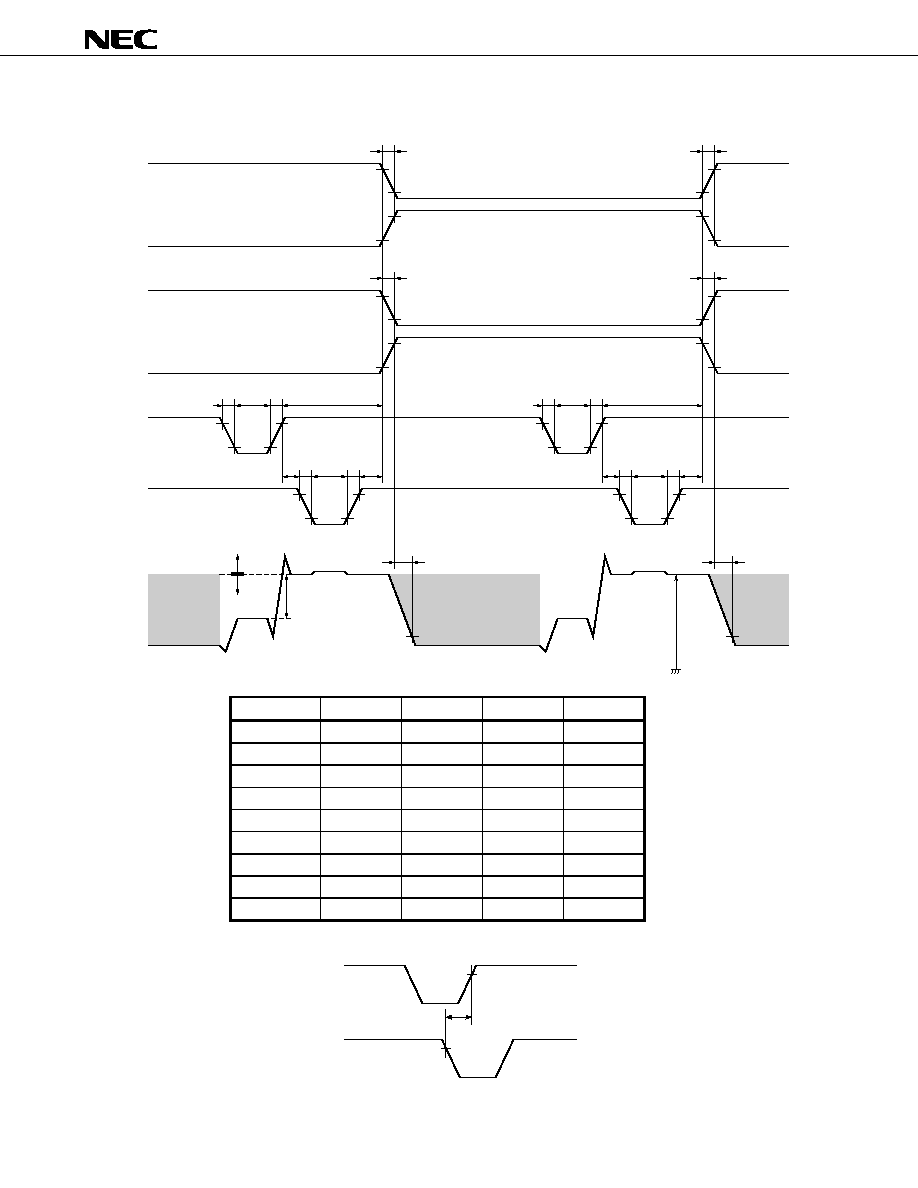
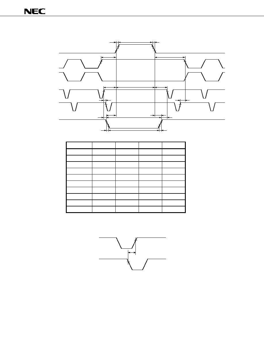
TIMING CHART 2
-
-
-
-1 (1200 dpi, bit clamp mode, for each color)
V
OUT
CLB
RB
2-1200
1-1200
90%
10%
90%
10%
90%
10%
RFTN
RFTN
≠
+
V
OS
t2
t1
t4
t6
t3
t5
t
d
10%
90%
10%
t10
t11
t8
t9
t7
2L
1L
90%
10%
90%
10%
t2'
t1'
t4
t6
t3
t5
t
d
t10
t11
t8
t9
t7
Symbol
Min.
Typ.
Max.
Unit
t1, t2
0
25
-
ns
t1', t2'
0
5
-
ns
t3
20
50
-
ns
t4
50
150
-
ns
t5, t6
0
5
-
ns
t7
-5
Note
+25
-
ns
t8
20
50
-
ns
t9, t10
0
5
-
ns
t11
5
25
-
ns
Note Min. of t7 shows that the
RB and
CLB overlap each other.
CLB
RB
90%
90%
t7
Data Sheet S16039EJ2V0DS
14
Ķ
Ķ
Ķ
Ķ
PD8891
TIMING CHART 2
-
-
-
-2 (1200 dpi, line clamp mode, for each color)
"H"
V
OUT
CLB
RB
2-1200
1-1200
90%
10%
90%
10%
90%
10%
V
OS
t2
t1
t4
t6
t3
t5
t
d
10%
2L
1L
90%
10%
90%
10%
t2'
t1'
t4
t6
t3
t5
t
d
RFTN
≠
+
RFTN
Symbol
Min.
Typ.
Max.
Unit
t1, t2
0
25
-
ns
t1', t2'
0
5
-
ns
t3
20
50
-
ns
t4
50
150
-
ns
t5, t6
0
5
-
ns
Data Sheet S16039EJ2V0DS
15
Ķ
Ķ
Ķ
Ķ
PD8891
TIMING CHART 2
-
-
-
-3 (600 dpi, even pixel, bit clamp mode, for each color)
V
OUT
CLB
90%
10%
90%
10%
V
OS
t2
t4
t6
t3'
t3'
t10
t8
t11
t7
t9
RB
2-1200
1-1200
90%
10%
90%
10%
t5
10%
t
d
+
RFTN
≠
90%
10%
90%
10%
t2'
2L
1L
t1
t1'
RFTN
Symbol
Min.
Typ.
Max.
Unit
t1, t2
0
25
-
ns
t1', t2'
0
5
-
ns
t3'
50
100
-
ns
t4
50
370
-
ns
t5, t6
0
5
-
ns
t7
-5
Note
+25
-
ns
t8
100
200
-
ns
t9, t10
0
5
-
ns
t11
5
100
-
ns
Note Min. of t7 shows that the
RB and
CLB overlap each other.
CLB
RB
90%
90%
t7
Data Sheet S16039EJ2V0DS
16
Ķ
Ķ
Ķ
Ķ
PD8891
TIMING CHART 2
-
-
-
-4 (600 dpi, even pixel, line clamp mode, for each color)
V
OUT
CLB
90%
10%
90%
10%
V
OS
t2
t4
t6
t3'
t3'
RB
2-1200
1-1200
90%
10%
t5
10%
t
d
+
RFTN
≠
90%
10%
90%
10%
t2'
2L
1L
t1
t1'
RFTN
"H"
Symbol
Min.
Typ.
Max.
Unit
t1, t2
0
25
-
ns
t1', t2'
0
5
-
ns
t3'
50
100
-
ns
t4
50
370
-
ns
t5, t6
0
5
-
ns
Data Sheet S16039EJ2V0DS
17
Ķ
Ķ
Ķ
Ķ
PD8891
TIMING CHART 2
-
-
-
-5 (600 dpi, odd pixel, bit clamp mode, for each color)
V
OUT
CLB
90%
10%
90%
10%
V
OS
t2
t4
t6
t3'
t3'
t10
t8
t11
t7
t9
RB
2-1200
1-1200
90%
10%
90%
10%
t5
10%
t
d
+
RFTN
≠
90%
10%
90%
10%
t2'
2L
1L
t1
t1'
RFTN
Symbol
Min.
Typ.
Max.
Unit
t1, t2
0
25
-
ns
t1', t2'
0
5
-
ns
t3'
50
100
-
ns
t4
50
370
-
ns
t5, t6
0
5
-
ns
t7
-5
Note
+25
-
ns
t8
100
200
-
ns
t9, t10
0
5
-
ns
t11
5
100
-
ns
Note Min. of t7 shows that the
RB and
CLB overlap each other.
CLB
RB
90%
90%
t7
Data Sheet S16039EJ2V0DS
18
Ķ
Ķ
Ķ
Ķ
PD8891
TIMING CHART 2
-
-
-
-6 (600 dpi, odd pixel, line clamp mode, for each color)
V
OUT
CLB
90%
10%
90%
10%
V
OS
t2
t4
t6
t3'
t3'
RB
2-1200
1-1200
90%
10%
t5
10%
t
d
+
RFTN
≠
90%
10%
90%
10%
t2'
2L
1L
t1
t1'
RFTN
"H"
Symbol
Min.
Typ.
Max.
Unit
t1, t2
0
25
-
ns
t1', t2'
0
5
-
ns
t3'
50
100
-
ns
t4
50
370
-
ns
t5, t6
0
5
-
ns
Data Sheet S16039EJ2V0DS
19
Ķ
Ķ
Ķ
Ķ
PD8891
TIMING CHART 2
-
-
-
-7 (300 dpi, bit clamp mode, for each color)
V
OUT
CLB
90%
10%
90%
10%
V
OS
t1
t4
t6
t3
t10
t8
t11
t7
t9
RB
2-300
1-300
90%
10%
90%
10%
t5
10%
t
d
+
RFTN
≠
t2
90%
10%
90%
10%
t1'
2L
1L
t2'
RFTN
Symbol
Min.
Typ.
Max.
Unit
t1, t2
0
25
-
ns
t1', t2'
0
5
-
ns
t3
20
50
-
ns
t4
50
150
-
ns
t5, t6
0
5
-
ns
t7
-5
Note
+25
-
ns
t8
20
50
-
ns
t9, t10
0
5
-
ns
t11
5
25
-
ns
Note Min. of t7 shows that the
RB and
CLB overlap each other.
CLB
RB
90%
90%
t7
Data Sheet S16039EJ2V0DS
20
Ķ
Ķ
Ķ
Ķ
PD8891
TIMING CHART 2
-
-
-
-8 (300 dpi, line clamp mode, for each color)
CLB
90%
10%
90%
10%
t1
t4
t6
t3
RB
2-300
1-300
90%
10%
t5
t2
90%
10%
90%
10%
t1'
2L
1L
t2'
"H"
V
OUT
V
OS
10%
t
d
+
RFTN
≠
RFTN
Symbol
Min.
Typ.
Max.
Unit
t1, t2
0
25
-
ns
t1', t2'
0
5
-
ns
t3
20
50
-
ns
t4
50
150
-
ns
t5, t6
0
5
-
ns
Data Sheet S16039EJ2V0DS
21
Ķ
Ķ
Ķ
Ķ
PD8891
TG1 to
TG3,
1,
2 TIMING CHART
RB
CLB
(Bit clamp mode)
TG1 to
TG3
CLB
(Line clamp mode)
1-1200
1-300,
2-1200
2-300,
10%
90%
90%
90%
90%
90%
90%
10%
t12
t13
t17
t7
t19
t9
t20
t10
t23
t21
t22
t11
Note 1
Note 2
t18
t16
t15
t14
Symbol
Min.
Typ.
Max.
Unit
t7
-5
Note 3
+25
-
ns
t9, t10
0
5
-
ns
t11
5
25
-
ns
t12
5000
10000
50000
ns
t13, t14
0
50
-
ns
t15, t16
900
1000
-
ns
t17, t18
200
400
-
ns
t19
t12
t12
50000
ns
t20, t21
0
50
-
ns
t22, t23
0
350
-
ns
Notes 1. Set the
RB pulse and
CLB pulse (bit clamp mode) to high level during this period.
2. Set the
RB pulse to high level during this period.
3. Min. of t7 shows that the
RB and CLB overlap each other.
CLB
RB
90%
90%
t7
Remark Inverse pulse of the
TG1 to
TG3 can be used as
CLB.
Data Sheet S16039EJ2V0DS
22
Ķ
Ķ
Ķ
Ķ
PD8891
1-300,
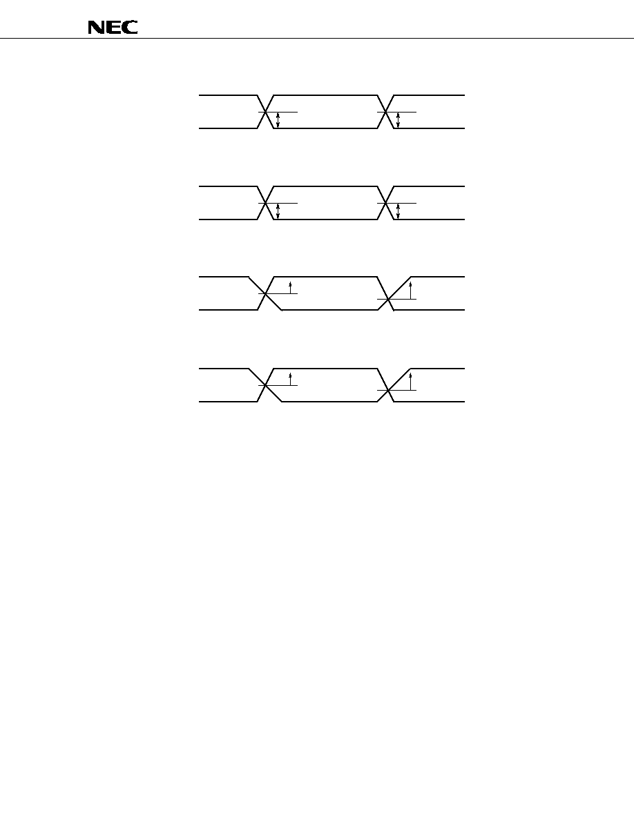
2-300 cross points
1-300
2-300
1.0 V to 4.0 V
1.0 V to 4.0 V
1-1200,
2-1200 cross points
1-1200
2-1200
1.0 V to 4.0 V
1.0 V to 4.0 V
1-300,
1-1200,
2L cross points
1-1200
1-300,
2L
2.0 V or more
0.5 V or more
2-300,
1-1200,
1L cross points
2-1200
2-300,
1L
2.0 V or more
0.5 V or more
Remark Adjust cross points (
1-300, 2-300), ( 1-1200, 2-1200), ( 1-300, 1-1200, 2L) and ( 2-300, 1-
1200,
1L) with input resistance of each pin.
Data Sheet S16039EJ2V0DS
23
Ķ
Ķ
Ķ
Ķ
PD8891
DEFINITIONS OF CHARACTERISTIC ITEMS
1. Saturation voltage : V
sat
Output signal voltage at which the response linearity is lost.
2. Saturation exposure : SE
Product of intensity of illumination (lx) and storage time (s) when saturation of output voltage occurs.
3. Photo response non-uniformity : PRNU
The output signal non-uniformity of all the valid pixels when the photosensitive surface is applied with the light
of uniform illumination. This is calculated by the following formula.
PRNU (%) =
x =
x
j
: Output voltage of valid pixel number j
x
x : maximum of
x
j
- x
x
Valid pixels
j = 1
Valid pixels
x
j
◊ 100
x
Register Dark
DC level
V
OUT
x
4. Average dark signal : ADS
Average output signal voltage of all the valid pixels at light shielding. This is calculated by the following
formula.
ADS (mV) =
d
j
: Dark signal of valid pixel number j
Valid pixels
j = 1
Valid pixels
d
j
Data Sheet S16039EJ2V0DS
24
Ķ
Ķ
Ķ
Ķ
PD8891
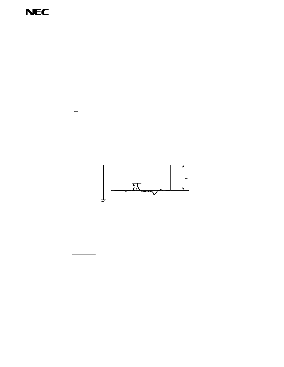
5. Dark signal non-uniformity : DSNU
Absolute maximum of the difference between ADS and voltage of the highest or lowest output pixel of all the
valid pixels at light shielding. This is calculated by the following formula.
d
j
: Dark signal of valid pixel number j
DSNU (mV) : maximum of
d
j
- ADS
j = 1 to valid pixels
ADS
DSNU
Register Dark
DC level
V
OUT
6. Output impedance : Z
O
Impedance of the output pins viewed from outside.
7. Response : R
Output voltage divided by exposure (lx∑s).
Note that the response varies with a light source (spectral characteristic).
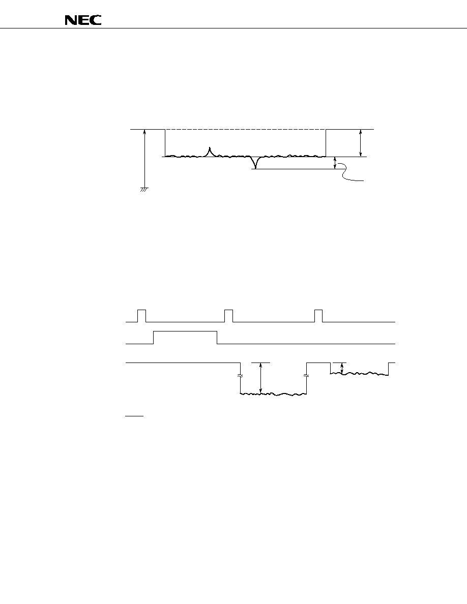
8. Image lag : IL
The rate between the last output voltage and the next one after read out the data of a line.
V
OUT
TG
Light
V
OUT
ON
OFF
V
1
IL (%) =
V
1
V
OUT
◊ 100
Data Sheet S16039EJ2V0DS
25
Ķ
Ķ
Ķ
Ķ
PD8891
9. Register Imbalance : RI (1200 dpi)
The rate of the difference between the averages of the output voltage of Odd and Even bits, against the
average output voltage of all the valid pixels.
RI (%) =
2
n
j = 1
j = 1
n
2
(V
2j ≠1
≠
V
2j
)
1
n
n
V
j
◊ 100
n
V
j
: Number of valid pixels
: Output voltage of each pixel
10. Random noise (CDS) :
CDS
Random noise
CDS is defined as the standard deviation of a valid pixel output signal with 100 times (=100
lines) data sampling at dark (light shielding).
CDS is calculated by the following procedure.
1. One valid photocell in one reading is fixed as measurement point.
2. The output level is measured during the reset feed-through period which is averaged over 100 ns to get
"VD
i
".
3. The output level is measured during the Video Output time averaged over 100 ns to get "VO
i
".
4. The correlated double sampling output is defined by VCDS
i
= VD
i
≠ VO
i
5. Repeat the above procedure (1 to 4) for 100 times (= 100 lines).
6. Calculate the standard deviation
CDS using the following formula equation.
CDS (mV) =
, V =
i
=
1
100
(VCDS
i
≠ V)
2
i
=
1
100
VCDS
i
100
100
1
Reset feed-through
Video output
Data Sheet S16039EJ2V0DS
26
Ķ
Ķ
Ķ
Ķ
PD8891
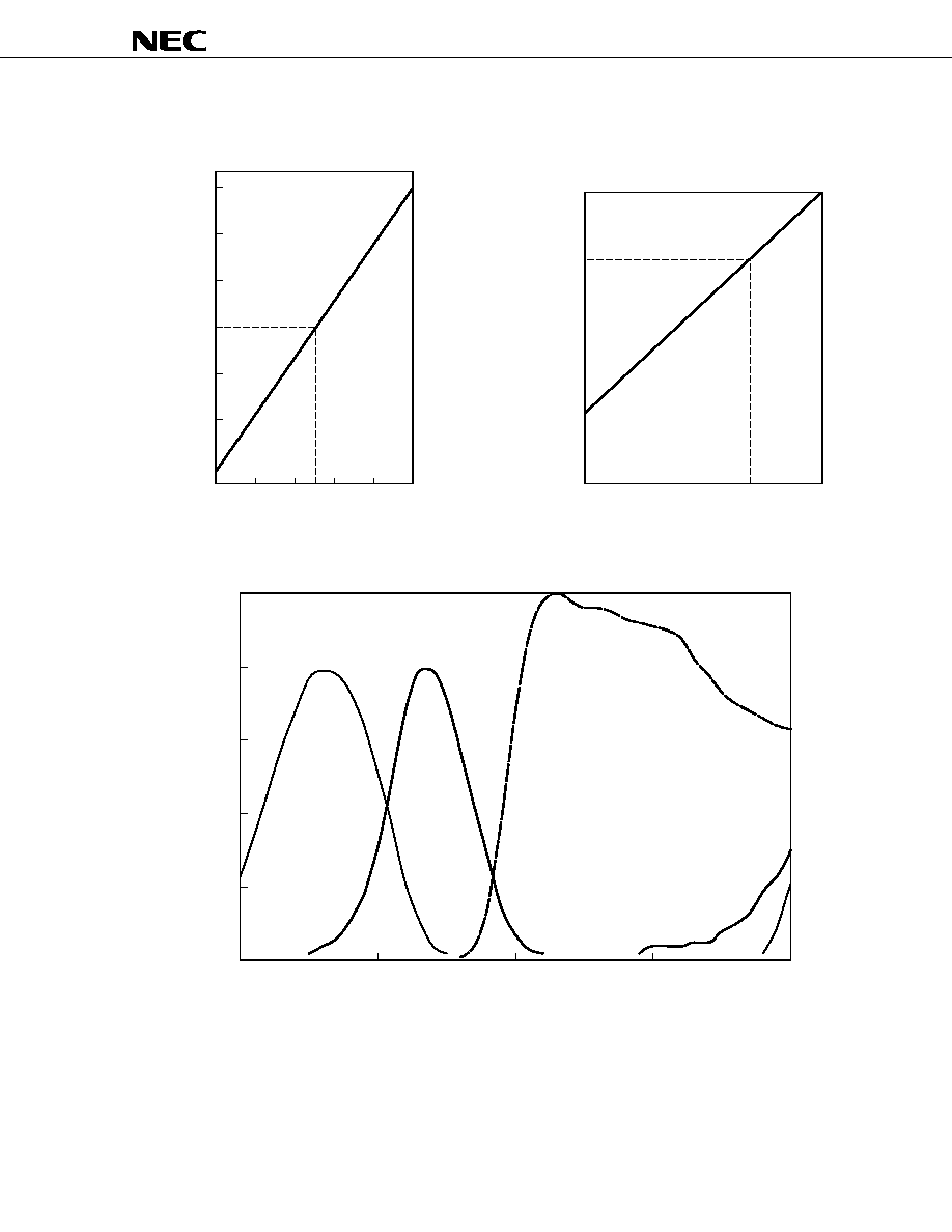
STANDARD CHARACTERISTIC CURVES (Reference Value)
DARK OUTPUT TEMPERATURE
CHARACTERISTIC
STORAGE TIME OUTPUT VOLTAGE
CHARACTERISTIC (T
A
= +25
įC)
Operating Ambient Temperature T
A
(
įC)
Storage Time (ms)
8
4
2
1
0.5
0.25
0.1
10
0
20
30
40
50
Relative Output Voltage
Relative Output Voltage
2
1
0.2
0.1
1
5
10
400
500
600
700
800
100
80
60
40
20
0
B
B
G
R
G
Response Ratio (%)
Wavelength (nm)
TOTAL SPECTRAL RESPONSE CHARACTERISTICS
(without infrared cut filter and heat absorbing filter ) (T
A
= +25
įC)
Data Sheet S16039EJ2V0DS
27
Ķ
Ķ
Ķ
Ķ
PD8891
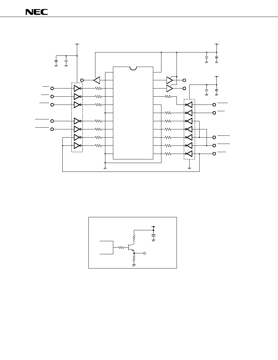
APPLICATION CIRCUIT EXAMPLE
+
PD8891
Ķ
+5 V
+12 V
+5 V
Ķ
0.1 F
Ķ
47 F/25 V
B2
B1
B3
47
1
2
3
4
5
6
7
8
9
10
11
22
21
20
19
18
17
16
15
14
13
12
150
150
150
4.7
4.7
4.7
4.7
10
NC
V
OUT
1
2-1200
1-1200
TG1
V
OUT
2
V
OUT
3
GND
RB
1L
2-300
1-300
2L
2-300
1-300
TG3
V
OD
SEL
TG
1L
2-300
1-300
SEL
GND
CLB
2-1200
1-1200
RB
2L
CLB
NC
TG2
47
+
Ķ
0.1 F
Ķ
10 F/16 V
+
Ķ
0.1 F
Ķ
10 F/16 V
4.7
10
10
4.7
Caution Connect the No connection pins (NC) to GND.
Remarks 1. The inverters shown in the above application circuit example are the 74HC04 (data rate
< 2 MHz) or
the 74AC04 (2
data rate < 5 MHz).
2. B1 to B3 in the application circuit example are shown in the figure blow.
47 F/25 V
B1 to B3 EQUIVALENT CIRCUIT
+
Ķ
12 V
100
100
CCD
V
OUT
2SC945
2 k
+
Data Sheet S16039EJ2V0DS
28
Ķ
Ķ
Ķ
Ķ
PD8891
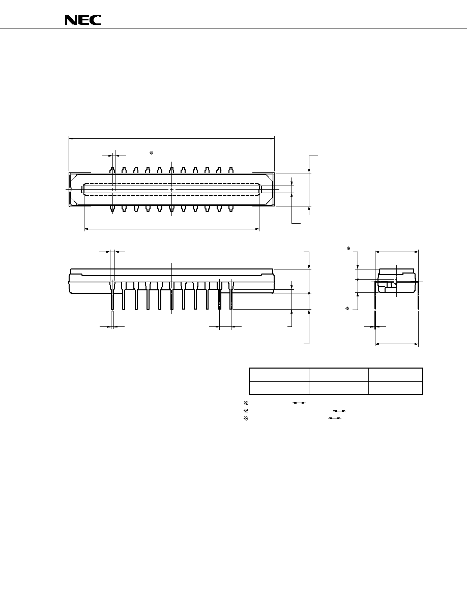
PACKAGE DRAWING
44.0
Ī
0.3
37.5
1st valid pixel
0.5
Ī
0.3
1
9.25
Ī
0.3
2.0
0.25
Ī
0.05
10.16
Ī
0.2
0.46
Ī
0.1
2.54
Ī
0.25
1.02
Ī
0.15
(5.42)
4.21
Ī
0.5
4.39
Ī
0.4
12
11
2.62
Ī
0.2
3
(1.72)
2
Name
Dimensions
Refractive index
Plastic cap
42.9
◊
8.35
◊
0.7
1.5
1 1st valid pixel The center of the pin1
2 The surface of the CCD chip The top of the cap
3 The bottom of the package The surface of the CCD chip
22C-1CCD-PKG11-1
(Unit : mm)
1
22
10.16
+
0.7
-
0.2
CCD LINEAR IMAGE SENSOR 22-PIN PLASTIC DIP (10.16 mm (400) )
PD8891CY
Ķ
Data Sheet S16039EJ2V0DS
29
Ķ
Ķ
Ķ
Ķ
PD8891
RECOMMENDED SOLDERING CONDITIONS
When soldering this product, it is highly recommended to observe the conditions as shown below.
If other soldering processes are used, or if the soldering is performed under different conditions, please make sure
to consult with our sales offices.
Type of Through-hole Device
Ķ
Ķ
Ķ
Ķ
PD8891CY : CCD linear image sensor 22-pin plastic DIP (10.16 mm (400))
Process
Conditions
Partial heating method
Pin temperature : 300
įC or below, Heat time : 3 seconds or less (per pin)
Cautions 1. During assembly care should be taken to prevent solder or flux from contacting the plastic
cap. The optical characteristics could be degraded by such contact.
2. Soldering by the solder flow method may have deleterious effects on prevention of plastic cap
soiling and heat resistance. So the method cannot be guaranteed.
Data Sheet S16039EJ2V0DS
30
Ķ
Ķ
Ķ
Ķ
PD8891
NOTES ON HANDLING THE PACKAGES
CLEANING THE PLASTIC CAP
DUST AND DIRT PROTECTING
MOUNTING OF THE PACKAGE
OPERATE AND STORAGE ENVIRONMENTS
Ethyl Alcohol
Methyl Alcohol
Isopropyl Alcohol
N-methyl Pyrrolidone
EtOH
MeOH
IPA
NMP
The optical characteristics of the CCD will be degraded if the cap is scratched during cleaning. Don't either
touch plastic cap surface by hand or have any object come in contact with plastic cap surface. Should dirt
stick to a plastic cap surface, blow it off with an air blower. For dirt stuck through electricity ionized air is
recommended. And if the plastic cap surface is grease stained, clean with our recommended solvents.
Care should be taken when cleaning the surface to prevent scratches.
We recommend cleaning the cap with a soft cloth moistened with one of the recommended solvents below.
Excessive pressure should not be applied to the cap during cleaning. If the cap requires multiple cleanings it is
recommended that a clean surface or cloth be used.
The following are the recommended solvents for cleaning the CCD plastic cap.
Use of solvents other than these could result in optical or physical degradation in the plastic cap.
Please consult your sales office when considering an alternative solvent.
The application of an excessive load to the package may cause the package to warp or break, or cause chips
to come off internally. Particular care should be taken when mounting the package on the circuit board. Don't
have any object come in contact with plastic cap. You should not reform the lead frame. We recommended to
use a IC-inserter when you assemble to PCB.
Also, be care that the any of the following can cause the package to crack or dust to be generated.
1. Applying heat to the external leads for an extended period of time with soldering iron.
2. Applying repetitive bending stress to the external leads.
3. Rapid cooling or heating
Operate in clean environments. CCD image sensors are precise optical equipment that should not be subject
to mechanical shocks. Exposure to high temperatures or humidity will affect the characteristics. So avoid
storage or usage in such conditions.
Keep in a case to protect from dust and dirt. Dew condensation may occur on CCD image sensors when the
devices are transported from a low-temperature environment to a high-temperature environment. Avoid such
rapid temperature changes.
For more details, refer to our document "Review of Quality and Reliability Handbook" (C12769E)
1
2
ELECTROSTATIC BREAKDOWN
CCD image sensor is protected against static electricity, but destruction due to static electricity is sometimes
detected. Before handling be sure to take the following protective measures.
1. Ground the tools such as soldering iron, radio cutting pliers of or pincer.
2. Install a conductive mat or on the floor or working table to prevent the generation of static electricity.
3. Either handle bare handed or use non-chargeable gloves, clothes or material.
4. Ionized air is recommended for discharge when handling CCD image sensor.
5. For the shipment of mounted substrates, use box treated for prevention of static charges.
6. Anyone who is handling CCD image sensors, mounting them on PCBs or testing or inspecting PCBs on
which CCD image sensors have been mounted must wear anti-static bands such as wrist straps and ankle
straps which are grounded via a series resistance connection of about 1 M
.
4
3
RECOMMENDED SOLVENTS
Solvents
Symbol
Data Sheet S16039EJ2V0DS
31
Ķ
Ķ
Ķ
Ķ
PD8891
NOTES FOR CMOS DEVICES
1
PRECAUTION AGAINST ESD FOR SEMICONDUCTORS
Note:
Strong electric field, when exposed to a MOS device, can cause destruction of the gate oxide and
ultimately degrade the device operation. Steps must be taken to stop generation of static electricity
as much as possible, and quickly dissipate it once, when it has occurred. Environmental control
must be adequate. When it is dry, humidifier should be used. It is recommended to avoid using
insulators that easily build static electricity. Semiconductor devices must be stored and transported
in an anti-static container, static shielding bag or conductive material. All test and measurement
tools including work bench and floor should be grounded. The operator should be grounded using
wrist strap. Semiconductor devices must not be touched with bare hands. Similar precautions need
to be taken for PW boards with semiconductor devices on it.
2
HANDLING OF UNUSED INPUT PINS FOR CMOS
Note:
No connection for CMOS device inputs can be cause of malfunction. If no connection is provided
to the input pins, it is possible that an internal input level may be generated due to noise, etc., hence
causing malfunction. CMOS devices behave differently than Bipolar or NMOS devices. Input levels
of CMOS devices must be fixed high or low by using a pull-up or pull-down circuitry. Each unused
pin should be connected to V
DD
or GND with a resistor, if it is considered to have a possibility of
being an output pin. All handling related to the unused pins must be judged device by device and
related specifications governing the devices.
3
STATUS BEFORE INITIALIZATION OF MOS DEVICES
Note:
Power-on does not necessarily define initial status of MOS device. Production process of MOS
does not define the initial operation status of the device. Immediately after the power source is
turned ON, the devices with reset function have not yet been initialized. Hence, power-on does
not guarantee out-pin levels, I/O settings or contents of registers. Device is not initialized until the
reset signal is received. Reset operation must be executed immediately after power-on for devices
having reset function.

Ķ
Ķ
Ķ
Ķ
PD8891
The information in this document is current as of March, 2003. The information is subject to change
without notice. For actual design-in, refer to the latest publications of NEC Electronics data sheets or
data books, etc., for the most up-to-date specifications of NEC Electronics products. Not all
products and/or types are available in every country. Please check with an NEC Electronics sales
representative for availability and additional information.
No part of this document may be copied or reproduced in any form or by any means without the prior
written consent of NEC Electronics. NEC Electronics assumes no responsibility for any errors that may
appear in this document.
NEC Electronics does not assume any liability for infringement of patents, copyrights or other intellectual
property rights of third parties by or arising from the use of NEC Electronics products listed in this document
or any other liability arising from the use of such products. No license, express, implied or otherwise, is
granted under any patents, copyrights or other intellectual property rights of NEC Electronics or others.
Descriptions of circuits, software and other related information in this document are provided for illustrative
purposes in semiconductor product operation and application examples. The incorporation of these
circuits, software and information in the design of a customer's equipment shall be done under the full
responsibility of the customer. NEC Electronics assumes no responsibility for any losses incurred by
customers or third parties arising from the use of these circuits, software and information.
While NEC Electronics endeavors to enhance the quality, reliability and safety of NEC Electronics products,
customers agree and acknowledge that the possibility of defects thereof cannot be eliminated entirely. To
minimize risks of damage to property or injury (including death) to persons arising from defects in NEC
Electronics products, customers must incorporate sufficient safety measures in their design, such as
redundancy, fire-containment and anti-failure features.
NEC Electronics products are classified into the following three quality grades: "Standard", "Special" and
"Specific".
The "Specific" quality grade applies only to NEC Electronics products developed based on a customer-
designated "quality assurance program" for a specific application. The recommended applications of an NEC
Electronics product depend on its quality grade, as indicated below. Customers must check the quality grade of
each NEC Electronics product before using it in a particular application.
"Standard": Computers, office equipment, communications equipment, test and measurement equipment, audio
and visual equipment, home electronic appliances, machine tools, personal electronic equipment
and industrial robots.
"Special":
Transportation equipment (automobiles, trains, ships, etc.), traffic control systems, anti-disaster
systems, anti-crime systems, safety equipment and medical equipment (not specifically designed
for life support).
"Specific": Aircraft, aerospace equipment, submersible repeaters, nuclear reactor control systems, life
support systems and medical equipment for life support, etc.
The quality grade of NEC Electronics products is "Standard" unless otherwise expressly specified in NEC
Electronics data sheets or data books, etc. If customers wish to use NEC Electronics products in applications
not intended by NEC Electronics, they must contact an NEC Electronics sales representative in advance to
determine NEC Electronics' willingness to support a given application.
(Note)
(1) "NEC Electronics" as used in this statement means NEC Electronics Corporation and also includes its
majority-owned subsidiaries.
(2) "NEC Electronics products" means any product developed or manufactured by or for NEC Electronics (as
defined above).
∑
∑
∑
∑
∑
∑
M8E 02. 11-1