MOS INTEGRATED CIRCUIT
µ
PD98402A
The
µ
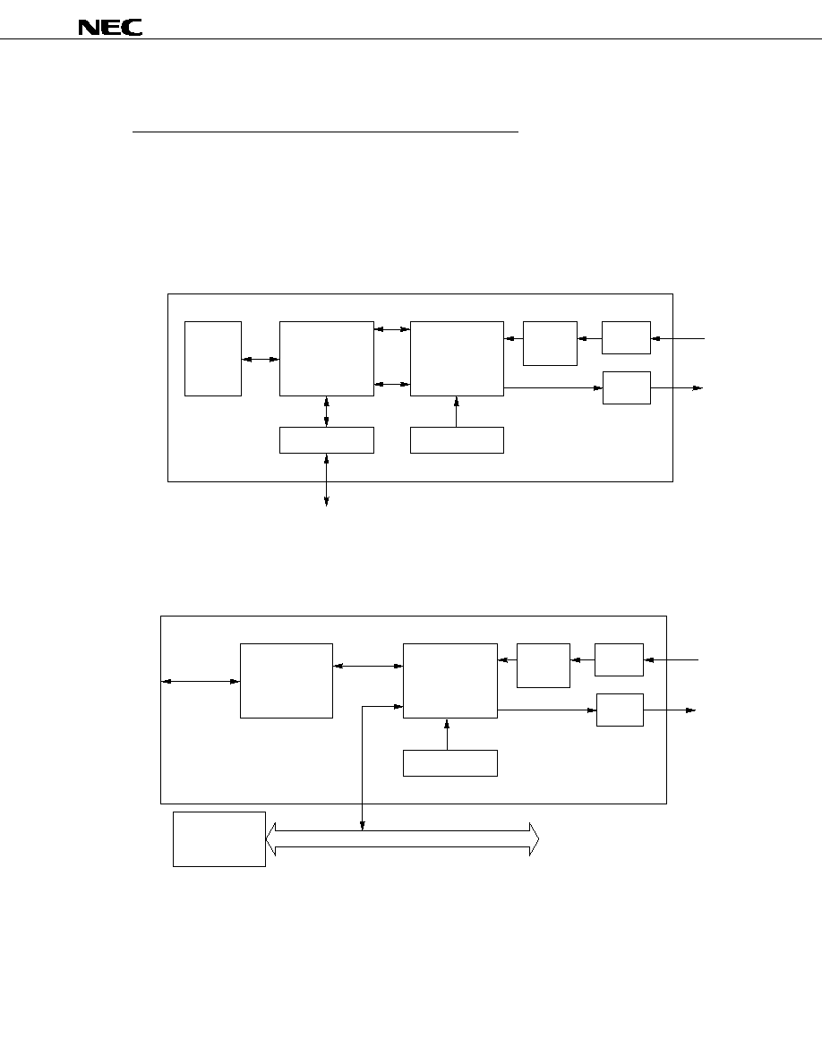
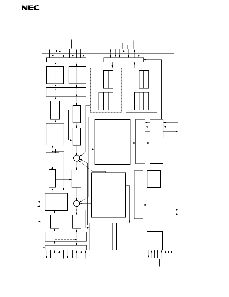
PD98402A is one of the ATM-LAN LSIs and incorporates the TC sublayer function in the SONET/SDH-
based physical layer of the ATM protocol. The main functions of the
µ
PD98402A include a transmit function for
mapping ATM cells received from the ATM layer onto the payload block of the SONET STS-3c/SDH STM-1 frame
and sending them to PMD (Physical Media Dependent) in the physical layer, and a receive function for separating
the overhead block and ATM cells from the data string received from the PMD sublayer and sending the ATM cells
to the ATM layer.
Futhermore, the
µ
PD98402A is compliant with the ATM Forum UNI Recommendations.
FEATURES
∑
Provision of TC sublayer function of ATM protocol physical layer
∑
Support of SONET STS-3c frame/SDH STM-1 frame format
∑
Provision of stop mode for cell scramble/descramble and frame scramble/descramble
∑
Disposal/transitory selection of unassigned cells is possible.
∑
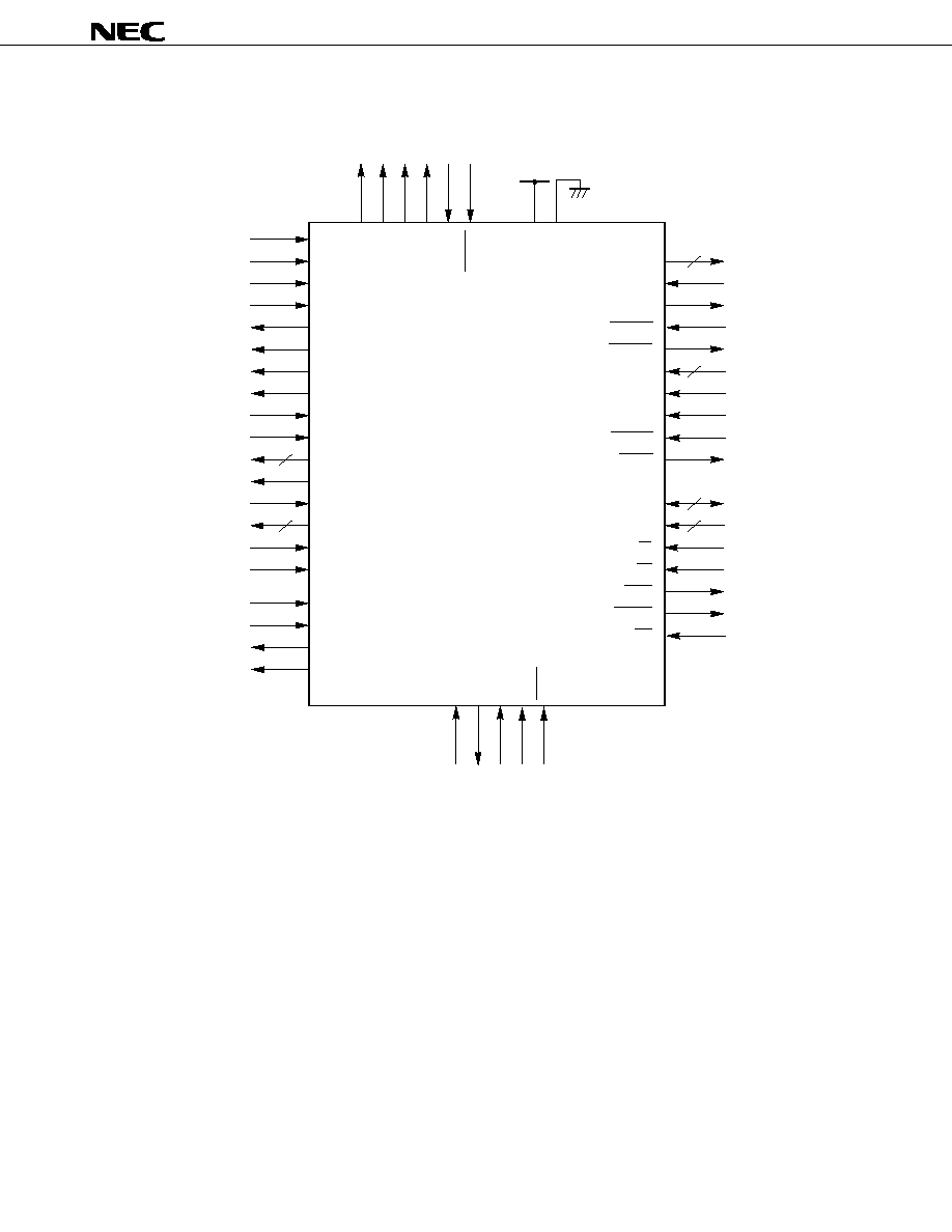
Compliant with UTOPIA interface
∑
Incorporation of internal loopback function at PMD and ATM layer turns
∑
PMD interface
155.52 Mbps serial interface
19.44 MHz parallel interface
∑
Provided with registers for writing/reading overhead information
SOH (section overhead): C1 (1st to 3rd) bytes, F1 byte
LOH (line overhead): K2 byte
POH (pass overhead): F2 byte, C2 byte
∑
CMOS process
∑
+5 V single power supply
LOCAL ATM SONET FRAMER
Document No. S10835EJ1V0DS00 (1st edition)
Date Published December 1995 P
Printed in Japan
The information in this document is subject to change without notice.
©
1995
DATA SHEET

µ
PD98402A
2
∑
Incorporation of OAM (Operation And Maintenance) function
Transmitting side
Transmission of various alarms
∑
Transmission by generation of sources
Line RDI (FERF), Path RDI (FERF)
Line FEBE, Path FEBE
∑
Transmission by command instruction
Line AIS, Path AIS
Line FEBE, Path FEBE
Receiving side
∑
Detection of alarms and error signals
LOS (Loss Of Signal)
OOF (Out Of Frame)
LOF (Loss Of Frame)
LOP (Loss Of Pointer)
LOC (Loss Of Cell delineation)
Line RDI (FERF), Path RDI (FERF)
Line AIS, Path AIS
∑
Detection and display of quality deterioration sources
B1 error, B2 error, B3 error, Line FEBE,
Path FEBE
∑
Incorporation of counter for counting number of performance
monitoring errors
B1 byte error counter
B2 byte error counter
B3 byte error counter
Line FEBE error counter
Path FEBE error counter