Document Outline
- COVER
- FEATURES
- ORDERING INFORMATION
- APPLICATIONS
- SYSTEM CONFIGURATION
- BLOCK DIAGRAM
- FUNCTIONAL PIN GROUPS
- PIN CONFIGURATION
- PIN ARRANGEMENT TABLE
- PIN NAME
- 1. PIN FUNCTIONS
- 1.1 PMD Interface
- 1.2 UTOPIA Interface
- 1.3 Management Interface
- 1.4 Alarm Signal Input/output
- 1.5 JTAG Boundary Scan
- 1.6 Power Supply and Ground
- 1.7 Others
- 1.8 Disipation of Unused Pins
- 1.9 Initial State of Pins
- 1.10 Correspondence between UTOPIA Interface Modes and Pins Used
- 2. ELECTRICAL CHARACTERISTICS
- 3. PACKAGE DRAWING
- 4. RECOMMENDED SOLDERING CONDITIONS
The information in this document is subject to change without notice. Before using this document, please
confirm that this is the latest version.
Not all devices/types available in every country. Please check with local NEC representative for
availability and additional information.
ATM QUAD SONET FRAMER
Document No. S12953EJ4V0DS00 (4th edition)
Date Published January 1999 NS CP(K)
Printed in Japan
©
NEC Corporation 1997,1999
MOS INTEGRATED CIRCUIT
µµµµ
PD98411
DATA SHEET
The
µ
PD98411 NEASCOT-P40 is one of ATM-LAN LSIs and provides the functions of the TC sublayer of the
SONET/SDH-base physical layer of the ATM protocol specified by the ATM Forum. Its main functions include a
transmission function to map an ATM cell passed from an ATM layer to the payload of 155M-bps SONET STS-
3c/SDH STM-1 frame and transmit the cell to the PMD (Physical Media Dependent) sublayer of the physical layer,
and a reception function to separate the overhead and ATM cell from the data string received from the PMD device
and transmit the ATM cell to the ATM layer. The
µ
PD98411 NEASCOT-P40 combines these transmission
/reception functions into a port function that is realized as a single 4-port LSI chip. This LSI is ideally suited for
use in the ATM hubs, ATM switches, and other equipment used to configure an ATM network.
In addition, the
µ
PD98411 also has a clock recovery function for each port to extract synchronous clock for
reception of receive data from the bit stream, and a clock synthesis function to generate a clock for transmission.
For the details of functional description, refer to the following user's manual.
µ
µ
µ
µ
PD98411 User's Manual : S12736E
FEATURES
∑
Incorporates an ATM user network interface TC sublayer function for four channels.
∑
Conforms to ATM FORUM UNI v3.1.
∑
Incorporates four clock recovery PLLs and one clock synthesizer PLL.
∑
Conforms to ATM FORUM UTOPIA Level 2 v1.0.
∑
ATM layers can be selected from the multi-PHY interface (up to 800 Mbps) in several different modes.
Single 16-bit
1TCLAV/1RCLAV (Cell Available signal mode)
Single 8-bit
Direct Status Indication mode
Dual 8-bit
Multiplexed Status Polling mode
∑
A management interface can be set to either of two modes.
RD-WR-RDY style (Intel-compatible mode)
DS-R/W-ACK style (Motorola-compatible mode)
∑
The line-side PMD interface accepts a P-ECL level input.
∑
Supports a loopback function.
∑
Supports a pseudo error generation frame transmission function.
∑
Incorporates one general input port per channel and three output ports (each able to drive an LED) per
channel.
∑
Supports JTAG boundary scan test (IEEE 1149.1).
Data Sheet S12953EJ4V0DS00
2
µ
µ
µ
µ
PD98411
∑
Incorporates a wide range of operation, administration, and maintenance (OAM) functions.
Transmission
Alarm Condition and Failure Detection
Line Quality Monitoring
APS
Insertion of B1-byte computation
Line AIS/Path AIS
Insertion of B2-byte computation
Line RDI/Path RDI
Insertion of B3-byte computation
Automatic transmission of a Line REI
Automatic transmission of a Path REI
Reception
Alarm Condition and Failure Detection
Notification of Degraded Line Quality
Line Quality Monitor Counter
External input signal change
B1 error
B1 error counter
LOS
B2 error
B2 error counter
OOF
B3 error
B3 error counter
LOF
Line REI
Line REI counter
LOP
Path REI
Path REI counter
OCD
Frequency justification
Frequency justification counter
LCD
FIFO overflow
HEC processing dropped cell counter
Line AIS/Path AIS
FIFO overflow dropped cell counter
Line RDI/Path RDI
Received idle cell counter
APS
Valid cell counter
∑
0.35-
µ
m CMOS process
∑
Low power consumption; +3.3 V single-voltage power supply
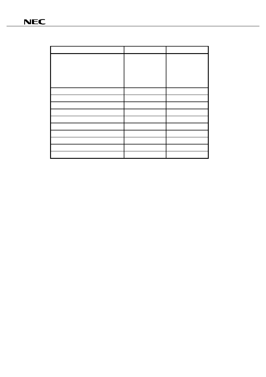
ORDERING INFORMATION
Part Number
Package
µ
PD98411GN-MMU
240-pin plastic QFP (fine pitch) (32
◊
32 mm)
Data Sheet S12953EJ4V0DS00
3
µ
µ
µ
µ
PD98411
APPLICATIONS
The following are examples of the application using the
µ
PD98411.
∑
∑
∑
∑
ATM Switches
NIC
NIC
NIC
µ
PD98411
UTOPIA Level2
CPU
SWITCH
155 ATM Interface
Backbone
Network
OC-12
SONET Framer
µ
PD98411
µ
PD98411
µ
PD98411
Data Sheet S12953EJ4V0DS00
4
µ
µ
µ
µ
PD98411
SYSTEM CONFIGURATION
1)
µ
µ
µ
µ
PD98411 System Application
µ
µ
µ
µ
PD98411
(NEASCOT-P40)
Processor
ATM Layer Device
Optical
Module
Optical
Module
Equalizer
Components
Equalizer
Components
Magnetics
RJ-45
Connector
Magnetics
RJ-45
Connector
OSC
(19.44M)
Shielded Twist Pair
Management I/F
Rx UTOPIA I/F
Multimode Fiber
Tx UTOPIA I/F
Status
PMD I/F
(PECL)
2) Connection to 5-V transceiver/receiver
The following show an example of connecting the
µ
PD98411 to a 5-V optical transceiver. Since the
µ
PD98411 operates on 3.3 V, a coupling circuit should be added if it is to be connected to a 5-V device.
820
110
110
510
820
91
91
Port0
RDIT0
RDIC0
TDOT0
TDOC0
SD0
RSDT
RSDC
TXDT
TXDC
VCCR
VCCT
VEER
VEET
SD
PECL->TTL
translator
MC10H350 by
Motorola, etc.
5V optical transceiver
5V
0.1
µ
F
0.1
µ
F
3.3V
GND
5V
510
GND
GND
0.1
µ
F
◊
4
430
430
82
130
1.1k
1.1k
82
GND
µ
PD98411
130
Data Sheet S12953EJ4V0DS00
5
µ
µ
µ
µ
PD98411
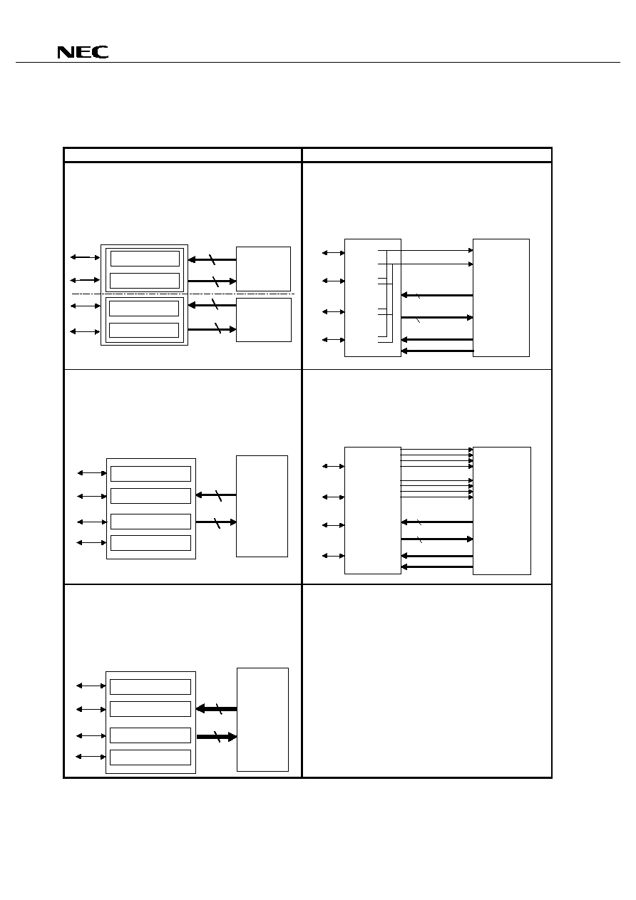
3) UTOPIA Interface
The UTOPIA interface transfers transmit/receive cell data to a device in the upper ATM layer. The interface
between the
µ
PD98411 and the ATM layer conforms to "MPHY Data Path Operation" of the "UTOPIA Level 2
version 1.0 June '95" standard.
Bus Mode
The way to indicate Cell Available state
Dual eight-bit bus.
In this mode, an 8-bit data bus is used for two ports. Ports 0
and 1 transfer signals using one eight-bit bus, while ports 2
and 3 transfer signals using another eight-bit bus. The ports
operate independently.
µ
PD98411
8-bit
ATM layer
device
8-bit
ATM layer
device
Port1
Port2
Port3
Port0
PMD
UTOPIA
One TCLAV & one RCLAV signal mode
The one TCLAV & one RCLAV signal mode outputs the TCLAV
and RCLAV signal status information for four ports of the
µ
PD98411 by multiplexing them into a single signal.
RADD
TADD
RDO
TCLAV
RCLAV
ATM layer
Device
µ
PD98411
Port0
Port1
Port2
Port3
TDI
8 or 16-bit
Single eight-bit bus.
In this mode, cell data for all four ports is transferred through
an eight-bit bus. The maximum transfer rate is 400 Mbps
(8 bits x 50 MHz).
µ
PD98411
8-bit
ATM layer
device
Port0
Port1
Port2
Port3
PMD
UTOPIA
Direct Status Indication Mode
µ
PD98411 has four TXCLAV and RXCLAV status signals, one
pair of TXCLAV and RXCLAV for each port. Status signals and
cell transfers are independent of each other. No address
information is needed to obtain status information.
8 or 16-bit
TDI
RCLAV3-RCLAV0
TCLAV3-TCLAV0
ATM layer
Device
µ
PD98411
Port0
Port1
Port2
Port3
RDO
RADD
TADD
Single sixteen-bit bus.
In this mode, cell data for all four ports is transferred through
a sixteen-bit bus. The maximum transfer rate is 800 Mbps
(16 bits x 50 MHz).
µ
PD98411
16-bit
ATM layer
device
Port0
Port1
Port2
Port3
PMD
UTOPIA
Multiplexed Status Polling Mode
When six or more
µ
PD98411s are connected to one ATM layer,
ATM layer obtain the status information of all the connected
ports in the 53 clock cycles in which it transmits or receives a
single data cell. Because a minimum of two clock cycles are
required to obtain the TCLAV/RCLAV signal status of a port by
ATM layer polling. Therefore every port address is allocated in a
fixed manner to one of the four status signals and to one of eight
port groups.
D
a
ta S
h
e
e
t S
1
29
53E
J
4
V
0
D
S
00
6
µ
µ
µ
µ
P
D
98
41
1
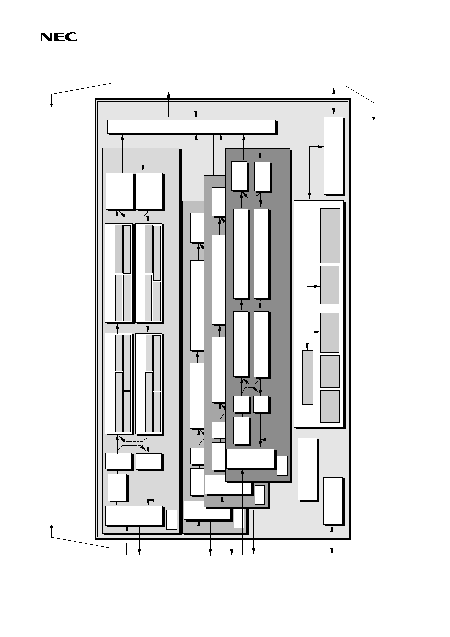
BLOCK DIAGRA
M
CPU Bus Interface
Address: 9 bits
Data: 8 bits
A
T
M
l
a
y
e
r i
n
t
e
rf
a
c
e
Management
interface
Tx/Rx overhead
registers
OAM sequencer
Interrupt cause
registers
Performance
registers
Mode
registers
JTAG
Clock
Recovery
RX FIFO
(8 cells)
P
M
D
i
n
te
rf
a
c
e
(
P
E
C
L
IN
/O
U
T
)
S/P
P/S
Rx timing generation
Rx framer block
BIP generation Overhead extraction
Descramble
Cell synchronization
HEC compare/control
Rx ATM cell processor block
Cell descramble
Idle cell drop
Tx timing generation
Tx framer block
BIP generation Overhead setup
Scramble
Cell mapping
HEC generation
Tx ATM cell processor block
Cell scramble
Idle cell insertion
TX FIFO
(8 cells)
Port0
Clock
Recovery
RX FIFO
P
M
D
i
n
te
rf
a
c
e
(
PECL I
N
/
O
UT)
S/P
P/S
Rx framer block
Rx ATM cell processor block
TX Framer Block
Tx ATM Cells Operate Block
Tx FIFO
6 Cells
Port1
Clock
recovery
RX FIFO
P
M
D
i
n
te
rf
a
c
e
(
PECL I
N
/
O
UT)
S/P
P/S
Rx framer block
Rx ATM cell processor block
TX Framer Block
Tx ATM Cells Operate Block
Tx FIFO
6 Cells
Port2
Clock
recovery
RX FIFO
P
M
D
i
n
te
rf
a
c
e
(
P
E
C
L
IN
/O
U
T
)
S/P
P/S
Rx framer block
Rx ATM cell processor block
Tx framer block
Tx ATM cell processor block
TX FIFO
Port3
Test
registers
Clock
Synthesizer
155.52 MHz
PECL
serial interface
Conforms to UTOPIA level 2 multi -PHY
interface of 400 to 800 Mbps
Data Sheet S12953EJ4V0DS00
7
µ
µ
µ
µ
PD98411
FUNCTIONAL PIN GROUPS
RCLK1
RSOC1
RCLAV1
RADD1[4:0]
RENBL1_B
RPR1
RADD2[4:0]
RCLAV2
RSOC2
RDO[15:0]
RCLK2
RENBL2_B
TCLK1
TSOC1
TCLAV1
TADD1[4:0]
TENBL1_B
TPR1
TADD2[4:0]
TCLAV2
TSOC2
TDI[15:0]
TCLK2
TENBL2_B
+3.3 V
GND
RDIT0/RDIC0 (differential input)
TDOT0/TDOC0 (differential input)
RDIT1/RDIC1 (differential input)
TDOT1/TDOC1 (differential input)
RDIT2/RDIC2 (differential input)
TDOT2/TDOC2 (differential input)
RDIT3/RDIC3 (differential input)
TDOT3/TDOC3 (differential input)
TFSS
TXFP
RXFP
RCL
TCL
REFCLK
MADD[8:0]
MDATA[7:0]
RW/WR_B
CS_B
RESET_B
BMODE
DS/RD_B
JC
K
JM
S
JD
I
J
R
STB
JD
O
VDD
PALM2[2:0]
PALM3[2:0]
PALM0[2:0]
PALM1[2:0]
CMD2
CMD3
CMD0
CMD1
SD2
SD3
SD0
SD1
PMD interface
UTOPIA interface
(Rx)
External alarm signal input
Alarm signal output
JTAG
boundary scan
interface
SD signal input
PHINT2_B
PHINT3_B
PHINT0_B
PHINT1_B
Management
interface
TFKT/TFKC (differential input)
CSSEL
UTOPIA interface
(Tx)
TPR2
RPR2
REFCLK-2nd
XLFC
RCLAV0
RCLAV3
TCLAV0
TCLAV3
ACK/RDY_B
Data Sheet S12953EJ4V0DS00
8
µ
µ
µ
µ
PD98411
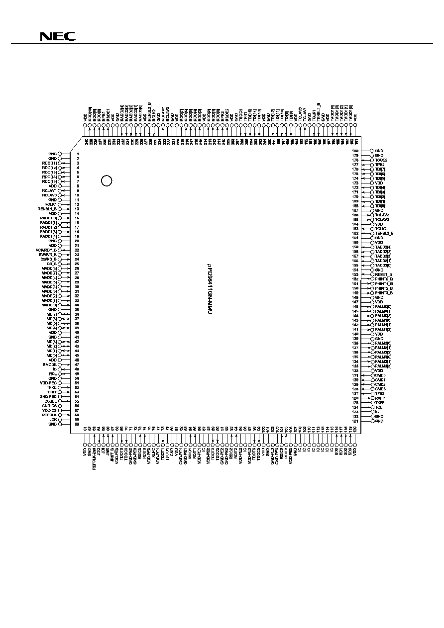
PIN CONFIGURATION
240-pin plastic QFP (fine pitch) (32
◊
32 mm) (Top View)
Remark1. IC: internal connect pin. Leave the IC pins open.
2. In this document, xxx_B stands for active low pin.

Data Sheet S12953EJ4V0DS00
9
µ
µ
µ
µ
PD98411
PIN ARRANGEMENT TABLE
(1/2)
Number
Pin Name
Number
Pin Name
Number
Pin Name
Number
Pin Name
1
GND
40
VDD
79
TDOC1
118
SD2
2
GND
41
GND
80
GND
119
SD3
3
RDO[11]
42
MD[3]
81
VDD
120
VDD
4
RDO[12]
43
MD[2]
82
GND-PE1
121
GND
5
RDO[13]
44
MD[1]
83
GND-PE1
122
GND
6
RDO[14]
45
MD[0]
84
RDIC1
123
IC
7
RDO[15]
46
VDD
85
RDIT1
124
TCL
8
VDD
47
BMODE
86
VDD-PE1
125
TXFP
9
RCLAV1
48
IC
87
IC
126
RXFP
10
RCLAV0
49
RCL
88
VDD-PE2
127
TFSS
11
GND
50
GND
89
TDOT2
128
CMD3
12
RCLK1
51
VDD-PEC
90
TDOC2
129
CMD2
13
RENBL1_B
52
TFKC
91
GND-PE2
130
CMD1
14
VDD
53
TFKT
92
GND-PE2
131
CMD0
15
RADD1[0]
54
GND-PEC
93
RDIC2
132
VDD
16
RADD1[1]
55
CSSEL
94
RDIT2
133
PALM3[2]
17
RADD1[2]
56
GND-CS
95
VDD-PE2
134
PALM3[1]
18
RADD1[3]
57
VDD-CS
96
IC
135
PALM3[0]
19
RADD1[4]
58
REFCLK
97
VDD-PE3
136
PALM2[2]
20
GND
59
JCK
98
TDOT3
137
PALM2[1]
21
VDD
60
GND
99
TDOC3
138
PALM2[0]
22
ACK/RDY_B
61
VDD
100
VDD
139
GND
23
RW/WR_B
62
GND
101
GND
140
VDD
24
DS/RD_B
63
REFCLK-2nd
102
GND-PE3
141
PALM1[2]
25
CS_B
64
JDO
103
GND-PE3
142
PALM1[1]
26
MADD[8]
65
JDI
104
RDIC3
143
PALM1[0]
27
MADD[7]
66
JMS
105
RDIT3
144
PALM0[2]
28
MADD[6]
67
JRST_B
106
VDD-PE3
145
PALM0[1]
29
MADD[5]
68
VDD-PE0
107
GND
146
PALM0[0]
30
MADD[4]
69
TDOT0
108
IC
147
VDD
31
MADD[3]
70
TDOC0
109
IC
148
GND
32
MADD[2]
71
GND-PE0
110
IC
149
PHINT3_B
33
MADD[1]
72
GND-PE0
111
IC
150
PHINT2_B
34
MADD[0]
73
RDIC0
112
IC
151
PHINT1_B
35
GND
74
RDIT0
113
IC
152
PHINT0_B
36
MD[7]
75
VDD-PE0
114
IC
153
RESET_B
37
MD[6]
76
XLFC
115
IC
154
GND
38
MD[5]
77
VDD-PE1
116
SD0
155
TADD2[0]
39
MD[4]
78
TDOT1
117
SD1
156
TADD2[1]

Data Sheet S12953EJ4V0DS00
10
µ
µ
µ
µ
PD98411
(2/2)
Number
Pin Name
Number
Pin Name
Number
Pin Name
Number
Pin Name
157
TADD2[2]
179
GND
201
VDD
223
RCLAV2
158
TADD2[3]
180
GND
202
TDI[13]
224
GND
159
TADD2[4]
181
VDD
203
TDI[14]
225
RCLK2
160
VDD
182
TADD1[0]
204
TDI[15]
226
RENBL2_B
161
GND
183
TADD1[1]
205
TPR1
227
VDD
162
TENBL2_B
184
TADD1[2]
206
TSOC1
228
RADD2[0]
163
TCLK2
185
TADD1[3]
207
GND
229
RADD2[1]
164
VDD
186
TADD1[4]
208
VDD
230
RADD2[2]
165
TCLAV3
187
VDD
209
RSOC2
231
RADD2[3]
166
TCLAV2
188
GND
210
RPR2
232
RADD2[4]
167
GND
189
TENBL1_B
211
RDO[0]
233
GND
168
TDI[0]
190
TCLK1
212
RDO[1]
234
VDD
169
TDI[1]
191
GND
213
RDO[2]
235
RSOC1
170
TDI[2]
192
TCLAV1
214
VDD
236
RPR1
171
TDI[3]
193
TCLAV0
215
RDO[3]
237
RDO[8]
172
TDI[4]
194
VDD
216
RDO[4]
238
RDO[9]
173
VDD
195
TDI[8]
217
RDO[5]
239
RDO[10]
174
TDI[5]
196
TDI[9]
218
RDO[6]
240
VDD
175
TDI[6]
197
TDI[10]
219
RDO[7]
176
TDI[7]
198
TDI[11]
220
VDD
177
TPR2
199
TDI[12]
221
GND
178
TSOC2
200
GND
222
RCLAV3

Data Sheet S12953EJ4V0DS00
11
µ
µ
µ
µ
PD98411
PIN NAME
ACK/RDY_B
: Acknowledge/Ready
REFCLK
: System Clock
BMODE
: Bus Mode
REFCLK-2nd
: 2nd Reference Cock
CMD3-CMD0
: Command Signal
CS_B
: Chip Select
RENBL2_B,
RENBL1_B
: Receive Data Enable
CSSEL
: Clock Source Select
RESET_B
: System Reset
DS/RD_B
: Data Strobe/Read
RPR2, RPR1
: Receive Data Path Parity
GND
: Ground
RSOC2, RSOC1 : Receive Start Of Cell
GND-CS
: Ground for Analog PLL Block
RW/WR_B
: Management Interface Read/Write
GND-PE3,
GND-PE2,
GND-PE1,
: Ground for Rx PECL Block
RxFP
SD3-SD0
TADD2[4:0],
: Receive Frame Pulse
: Signal Detect
: Transmit Address
GND-PE0
TADD1[4:0]
GND-PEC
: Ground for TFKT/C PECL Block
TCL
: Internal Transmit System Clock
JCK
: JTAG Clock
TCLAV3-TCLAV0 : Transmit Cell Available Signals
JDI
: JTAG Data Input
TCLK2, TCLK1
: Transmit DATA transferring Clock
JDO
: JTAG Data Output
JMS
: JTAG Mode Select
TDI15-TDI0
: Transmit Data Input from the ATM
Layer
JRST_B
: JTAG Reset
TDOC3-TDOC0
: Transmit Data Output Complement
TDOT3-TDOT0
: Transmit Data Output True
MADD[8:0]
: Management Interface Address
Bus
TENBL2_B,
: Transmit Data Enable
MD[7:0]
: Management Interface Data Bus
TENBL1_B
TFKC
TFKT
TFSS
: Transmit Reference Clock Complement
: Transmit Reference Clock True
: Transmit Frame Set Signal
PALM3[2:0],
PALM2[2:0],
PALM1[2:0],
PALM0[2:0]
: Physical Alarm Output Signals
TPR2,TPR1
: Transmit Data Path Parity
TSOC2,TSOC1
: Transmit Start Of Cell
PHINT3_B,
PHINT2_B,
PHINT1_B,
PHINT0_B,
: Physical Interrupt
TxFP
VDD
VDD-CS
: Transmit Frame Pulse
: Supply Voltage
: Supply Voltage for Analog PLL Block
RADD2[4:0],
RADD1[4:0]
RCL
RCLAV3-RCLAV0
: Receive Address
: Internal Receive System Clock
: Receive Cell Available Signals
VDD-PE3,
VDD-PE2,
VDD-PE1,
VDD-PE0
: Supply Voltage for Rx PECL Block
VDD-PEC
: Supply Voltage for TFKT/C PECL
Block
XLFC
: Tx Loop Filter Capacity
RCLK2, RCLK1
RDIC3-RDIC0
RDIT3-RDIT0
RDO[15:0]
: Receive Data Transferring Clock
: Receive Data Input Complement
: Receive Data Input True
: Receive Data Output

Data Sheet S12953EJ4V0DS00
12
µ
µ
µ
µ
PD98411
CONTENTS
1. PIN FUNCTIONS ..............................................................................................
1.1 PMD Interface ...............................................................................................................
1.2 UTOPIA Interface ..........................................................................................................
1.3 Management Interface ...................................................................................................
1.4 Alarm Signal Input/output ................................................................................................
1.5 JTAG Boundary Scan ....................................................................................................
1.6 Power Supply and Ground ...............
´´´´´´´´´´´´´´´´´´´´´´´´´´1
1.7 Others ........................................................................................................................
1.8 Disipation of Unused Pins ...............................................................................................
1.9 Initial State of Pins ........................................................................................................
1.10 Correspondence between UTOPIA Interface Modes and Pins Used .........................................
2. ELECTRICAL CHARACTERISTICS .......................................................................
3. PACKAGE DRAWING ..........................................................................................
4. RECOMMENDED SOLDERING CONDITIONS .........................................................
13
13
15
19
20
20
21
21
22
23
24
25
33
34
Data Sheet S12953EJ4V0DS00
13
µ
µ
µ
µ
PD98411
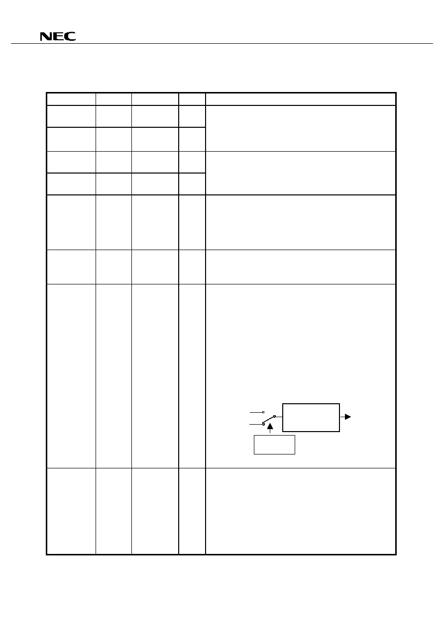
1. PIN FUNCTIONS
1.1 PMD Interface
(1/3)
Pin Name
Pin No.
I/O Level
I/O
Function
RDIT3-
RDIT0
105, 94,
85, 74
P-ECL
True(+)
I
RDIC3-
RDIC0
104, 93,
84, 73
P-ECL
Complement(-)
I
Receive serial data input.
Refers to the differential input of the P-ECL level.
TDOT3-
TDOT0
98, 89,
78, 69
P-ECL
True(+)
O
TDOC3-
TDOC0
99, 90,
79, 70
P-ECL
Complement(-)
O
Transmit serial data output.
Refers to the differential output of the P-ECL level. To the transmit
clock.
SD3-SD0
119-116
CMOS
I
Line signal detection signal input.
Refers to the pins for inputting the SD (Signal Detect) signal of
line transceivers (such as optical modules). If this signal goes low,
this port detects LOS.
High: Normal
Low: LOS state
REFCLK
58
CMOS
I
System clock (19.44MHz) input.
Used as the source clock for the internal synthesizer PLL/clock
recovery PLL and register operation.
REFCLK-2nd
63
CMOS
I
Second system clock (19.44MHz) input.
Refers to the pin for inputting the second source clock of the
internal synthesizer PLL. This pin is not used if it is unnecessary
to switch the source clock of the synthesizer PLL. The CSSC
register (address 076H) specifies which of REFCLK and
REFCLK-2nd clocks to use as the source block. The REFCLK
input is selected as the default. Even when REFCLK-2nd is used
as the source clock of the synthesizer PLL, REFCLK is used for
register operation as well; therefore, it is necessary to input the
clock.
RXFP
126
CMOS
O
Receive frame pulse output (8kHz).
The pulse signal is output synchronously with the start of the
receiving frame. The pulse signal is 1 cycle of the RCL clock in
length.
The internal FPMSK register (address: 07CH) is used to select
which of the four ports will output the pulse synchronous to the
receiving frame. No port is selected as the default; therefore,
using the default will result in no output.
Transmit synthesizer
PLL clock
155.52MHz
transmit clock
Register
REF_cnt bit
REFCLK
REFCLK_2nd

Data Sheet S12953EJ4V0DS00
14
µ
µ
µ
µ
PD98411
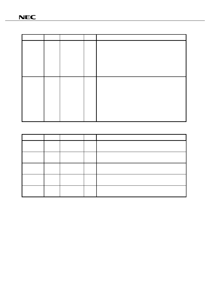
(2/3)
Pin Name
Pin No.
I/O Level
I/O
Function
XLFC
76
Analog
O
Loop filter capacity connection pin.
Refers to the pin connecting the loop filter of the synthesizer PLL.
Leave the pin open.
TXFP
125
CMOS
O
Transmitting end frame pulse signal output (8KHz).
Outputs a pulse signal synchronous with the start of the
transmission frame and equivalent to the 1 cycle of the TCL clock
in length. The setting of the internal FPMSK register (address:
07CH) selects which of the four ports should output the pulse
synchronous with the transmitting frame. No port is selected as
the default value; therefore, using the default will result in no
output.
TFSS
127
CMOS
I
Frame transmission disable signal input.
If High is input to this pin, the output data strings of all ports are
fixed to either to 0 or 1 and frame transmission stops. If Low is
input, transmission restarts from the start (the 1st A1 byte) of the
frame. Transmission starts with the output of a transmission
synchronously with the rising edge of the TCL clock 9 cycles after
the last rising edge of the TCL clock at which TFSS was detected
as being high.
RCL
49
CMOS
O
Receive system clock output (19.44MHz).
Each port uses the 155.52MHz receive clock divided by eight for
internal receive processing; and this pin outputs this clock. Which
port's system clock is output is selected by setting the relevant
value of the RCMSK register (address: 07BH). By using the
default value, the clock of port 0 is selected. During resetting or
when no port is selected, Low is output. Also, this pin can output
REFCLK-2nd clock.

Data Sheet S12953EJ4V0DS00
15
µ
µ
µ
µ
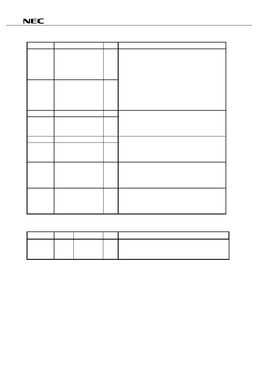
PD98411
# # # # # # # # # # #
(3/3)
Pin Name
Pin No.
I/O Level
I/O
Function
TCL
124
CMOS
O
Transmission system clock output (19.44 MHz).
Each port uses the 155.52MHz transmit clock divided by eight for
internal transmit processing; and this pin outputs this clock.
Which port's system clock is output is selected by setting the
relevant value of the TCMSK register (address: 07AH). During
resetting or when no port is selected, Low is output.
TFKT
53
P-ECL
True(+)
I
TFKC
52
P-ECL
Complement(-)
I
Externally generated 155.52MHz transmit clock input.
Refers to the pin for inputting the externally generated transmit
clock (155.52MHz) when not using the internally mounted
synthesizer PLL. This pin is enabled by setting the CSSEL pin to
High.
CSSEL
55
CMOS
I
TFKT/TFKC pin enable signal input.
This pin inputs the enable signal of the TFKT/TFKC pin when
inputting a 155.52MHz clock from outside the chip at the
TFKT/TFKC pin.
High: TFKT/TFKC pin enable
Low: TFKT/TFKC pin disable
1.2 UTOPIA Interface
The pin used for each UTOPIA interface signal varies with the mode selected by the internal MltUt register (at
address 079H). Please refer the table "Correspondence between UTOPIA Interface Modes and Pins Used".
(1/4)
Pin Name
Pin No.
I/O Level
I/O
Function
RDO[15:8]
RDO[7:0]
7-3
239-237
219-215
213-211
CMOS
O
3-state
Receive data buses.
These 16-bit data bus pins transfer receive data to the ATM
layer device. Output is made synchronous with the startup of
the RCLK clock. The pins used varies depending on the
UTOPIA interface mode selected by the MltUt register
(address: 079H).
∑
Single 8-bit bus: RDO[7:0]
∑
Single 16-bit bus: RDO[15:0]
∑
Dual 8-bit bus: RDO[15:8]/RDO[7:0]
RCLK2
RCLK1
225
12
CMOS
I
Receive clock input.
These pins accept receive data transfer clocks of up to
50MHz. The pin to be used varies depending on the UTOPIA
interface mode selected by the MltUt register (address: 079H).
∑
Single 8-bit bus: RCLK2
∑
Single 16-bit bus: RCLK1
∑
Dual 8-bit bus: RCLK1/RCLK2

Data Sheet S12953EJ4V0DS00
16
µ
µ
µ
µ
PD98411
(2/4)
Pin Name
Pin No.
I/O Level
I/O
Function
RSOC2
RSOC1
209
235
CMOS
O
3-state
Receive cell starting location signal output.
These pins output a signal which indicates the location of the first
byte with regard to the ATM layer device. The pin to be used
varies depending on the UTOPIA interface mode selected by the
MltUt register (address: 079H).
∑
Single 8-bit bus: RSOC2
∑
Single 16-bit bus: RSOC2
∑
Dual 8-bit bus: RSOC1/RSOC2
RENBL2_B
RENBL1_B
226
13
CMOS
I
Receive enable signal input.
These pins input a signal which indicates that the corresponding
ATM layer device is capable of accepting receive data. The pin to
be used varies depending on the UTOPIA interface mode
selected by the MltUt register (address: 079H).
∑
Single 8-bit bus: RENBL2_B
∑
Single 16-bit bus: RENBL1_B
∑
Dual 8-bit bus: RENBL1_B/RENBL2_B
RCLAV3
RCLAV2
RCLAV1
RCLAV0
222
223
9
10
CMOS
O
3-state
Receive cell transferable signal output.
This signal informs the ATM layer device that 1 cell or more of
data exists in the receive FIFO.
In 1TCLAV&1RCLAV mode, the RCLAV signal of each port is
internally multiplexed to be output as a signal. Of the four signals
of RCLAV0 to RCLAV3, the pin and operation of the signal which
is used vary depending on the UTOPIA interface mode selected
by the MltUt register (address: 079H).
∑
Single 8-bit bus: RCLAV2
∑
Single 16-bit bus: RCLAV1
∑
Dual 8-bit bus: RCLAV1/RCLAV2
In Direct Status Indication (DSI) mode, the four signals of
RCLAV0 to RCLAV3 are allocated to each of the ports to identify
their FIFO statuses. RCLAV0 corresponds to Port 0, and RCLAV3
to Port 3.
RADD2[4:0]
RADD1[4:0]
232-228
19-15
CMOS
I
Receiving end PHY address input.
These pins input the address which selects the port. Different
pins are used depending on the UTOPIA interface mode selected
by the MltUt register (address: 079H).
∑
Single 8-bit bus: RADD2[4:0]
∑
Single 16-bit bus: RADD1[4:0]
∑
Dual 8-bit bus: RADD1[4:0]/RADD2[4:0]

Data Sheet S12953EJ4V0DS00
17
µ
µ
µ
µ
PD98411
(3/4)
Pin Name
Pin No.
I/O Level
I/O
Function
RPR2
RPR1
210
236
CMOS
O
Parity bit output pins.
Odd parity bits are generated and output from these pins with
respect to the data output from RDO15-RDO0. The pin to be used
varies depending on the UTOPIA interface mode selected by the
MltUt register (address: 079H).
∑
Single 8-bit bus: RPR2
∑
Single 16-bit bus: RPR2
∑
Dual 8-bit bus: RPR1/RPR2
TDI[15:8]
TDI[7:0]
204-202
199-195
176-174
172-168
CMOS
I
Transmit data buses.
These data buses input transmit data from the ATM layer device
at the rising edge of the TCLK clock.
The pin to be used varies depending on the UTOPIA interface
mode selected by the MltUt register (address: 079H).
∑
Single 8-bit bus: TDI[15:8]
∑
Single 16-bit bus: TDI[15:0]
∑
Dual 8-bit bus: TDI[15:8]/TDI[7:0]
TCLK2
TCLK1
163
190
CMOS
I
Transmit clock input.
These pins input clocks of up to 50MHz for transmit data transfer.
The pin to be used varies depending on the UTOPIA interface
mode selected by the internal MltUt register (address: 079H).
∑
Single 8-bit bus: TCLK1
∑
Single 16-bit bus: TCLK2
∑
Dual 8-bit bus: TCLK1/TCLK2
TSOC2
TSOC1
178
206
CMOS
I
Transmit cell starting location signal input.
These pins input a signal which indicates the location of the first
byte of the transmit cell.
The pin to be used varies depending on the UTOPIA interface
mode selected by the MltUt register (address: 079H).
∑
Single 8-bit bus: TSOC1
∑
Single 16-bit bus: TSOC1
∑
Dual 8-bit bus: TSOC1/TSOC2
TENBL2_B
TENBL1_B
162
189
CMOS
I
Transmit enable signal input.
These pins input a signal which indicates that the ATM layer
device is outputting valid transmit data to TDI[15]-TDI[0]. The pin
to be used varies depending on the UTOPIA interface mode
selected by the internal MltUt register (address: 079H).
∑
Single 8-bit bus: TENBL1_B
∑
Single 16-bit bus: TENBL2_B
∑
Dual 8-bit bus: TENBL1_B/TENBL2_B

Data Sheet S12953EJ4V0DS00
18
µ
µ
µ
µ
PD98411
(4/4)
Pin Name
Pin No.
I/O Level
I/O
Function
TCLAV3
TCLAV2
TCLAV1
TCLAV0
165
166
192
193
CMOS
O
3-state
Transmit cell acceptable signal output.
The signal informs the ATM layer device that unused storage
space of at least 1 cell is available in the transmit FIFO.
In 1TCLAV&1RCLAV mode, the TCLAV signal of each port is
internally multiplexed to be output as a signal. Of the four signals
of TCLAV0 to TCLAV3, the pin to be used varies depending on
the UTOPIA interface mode selected by the MltUt register
(address: 079H).
∑
Single 8-bit bus: TCLAV1
∑
Single 16-bit bus: TCLAV2
∑
Dual 8-bit bus: TCLAV1/TCLAV2
In Direct Status Indication (DSI) mode, the four pins TCLAV0 to
TCLAV3 are allocated to each of the ports signal by signal, and
indicate the FIFO statuses of each port. TCLAV0 corresponds to
Port 0; and TCLAV3 to Port 3.
TADD2[4:0]
TADD1[4:0]
159-155
186-182
CMOS
I
Transmission PHY address input.
These pins input the address of the port to be selected. The pins
used vary depending on the UTOPIA interface mode selected by
the MltUt register (address: 079H).
∑
Single 8-bit bus: TADD1[4:0]
∑
Single 16-bit bus: TADD2[4:0]
∑
Dual 8-bit bus: TADD1[4:0]/TADD2[4:0]
TPR2
TPR1
177
205
CMOS
I
Parity bit input pins.
These pins input the odd parity bit input from TD0[15]-TDO[0].
The pin to be used varies depending on the UTOPIA interface
mode selected by the MltUt register (address: 079H).
∑
Single 8-bit bus: TPR1
∑
Single 16-bit bus: TPR1
∑
Dual 8-bit bus: TPR1/TPR2

Data Sheet S12953EJ4V0DS00
19
µ
µ
µ
µ
PD98411
1.3 Management Interface
Pin Name
Pin No.
I/O Level
I/O
Function
BMODE
47
CMOS
I
Mode selection input.
This pin input is used to select the mode of the management
interface.
BMODE=:
1: Selects <RD_B, WR_B, RDY_B> as the pin function.
0: Selects <DS_B, R/W_B, ACK_B> as the pin function.
MADD[8:0]
26-34
CMOS
I
Address input.
9-bit addresses for inputting internal register addresses.
MD[7:0]
36-39
42-45
CMOS
I/O
3-state
8-bit data buses for reading/writing internal register data.
CS_B
25
CMOS
I
Chip select signal input.
When at low level, access to internal registers is enabled.
DS/RD_B
24
CMOS
I
Data strobe signal input or read signal input.
The function of this pin varies depending on the management
interface mode selected for the BMODE pin input.
BMODE =0: Functions as data strobe signal DS_B
BMODE =1: Function as RD_B selecting the read access
RW/WR_B
23
CMOS
I
Read/write signal input or write signal input.
The function of this pin varies depending on the management
interface mode selected for the BMODE pin input. When
BMODE=0, the pin functions as Read/Write control signal
R/W_B.
R/W_B= High:
Read cycle
Low:
Write cycle
When BMODE=1, the pin functions as WR_B selecting Write for
internal registers.
ACK/RDY_B
22
CMOS
O
3-state
Data acknowledge signal output or ready signal output.
Outputs acknowledge and ready signals which accept the
Read/Write cycle for internal registers.
PHINT3_B-
PHINT0_B
149-152
CMOS
O
Interrupt signal output.
These signals inform the host that an interrupt factor has
occurred. Two modes are available for this purpose: one which
indicates an interrupt factor for four ports using the PHINT0_B
signal and the other which uses four pins PHINT0-PHINT3 to
indicate an individual interrupt for each port. Port 0 corresponds
to the PHINT0_B pin; and Port 3 to PHINT3_B.
RESET_B
153
CMOS
I
System reset signal input.
Initializes the
µ
PD98411. This input signal should be kept low for
1
µ
s or more. Especially, in case of the power on, above-
mentioned pulse width must be kept after the supply voltage
reaches equal to or more than 90% at least. When the
RESET_B signal is input, the clock must be input at REFCLK pin.
Data Sheet S12953EJ4V0DS00
20
µ
µ
µ
µ
PD98411
1.4 Alarm Signal Input/output
Pin Name
Pin No.
I/O Level
I/O
Function
CMD0-CMD3
128-131
CMOS
I
General-purpose input signal.
Refers to the general-purpose input pins which input the status
signals, etc. from external peripheral devices. The signal level of
these pins can also be reflected in the status bits of internal
registers, and changes in these bits can be used identify
interrupt factors. Each port is equipped with a pin: CMD0
corresponds to Port 0 and CMD3 to Port 3.
PALM3[2:0]
PALM2[2:0]
PALM1[2:0]
PALM0[2:0]
133-135
136-138
141-143
144-146
CMOS
O
PHY layer alarm detection signal output.
These pins output the signal to notify that the port detected the
alarm or the defect (LOS, OOF, LOF, LOP, OCD, LCD, Line AIS,
Path AIS, Line RDI, Path RDI) or that the level of the CMD pin
input was changed. Additionary, it is possible to use as the
general output ports which reflects state of the bit of the internal
register,too.
The events to be indicated are selected by seting to AMPR,
AMR1, AMR2 registers.
1.5 JTAG Boundary Scan
Pin Name
Pin No.
I/O Level
I/O
Function
JDI
65
CMOS
I
Refers to the boundary scan data input.
When unused, connect this to ground.
JDO
64
CMOS
O
3-state
Refers to the boundary scan data output.
When unused, leave this open.
JCK
59
CMOS
I
Refers to the boundary scan clock input.
When unused, connect this to ground.
JMS
66
CMOS
I
Refers to the boundary scan mode select signal input.
When unused, connect this to ground.
JRST_B
67
CMOS
I
Refers to the boundary scan reset signal input.
When unused, connect this to ground.
Data Sheet S12953EJ4V0DS00
21
µ
µ
µ
µ
PD98411
1.6 Power Supply and Ground
Pin Name
Pin No
I/O
Function
VDD
8, 14, 21, 40, 46, 61, 81,
100, 120, 132, 140, 147,
160, 164, 173, 181, 187,
194, 201, 208, 214, 220,
227,
234,
240
--
GND
1 ,2, 11, 20, 35, 41, 50,
60, 62, 80, 101, 107, 121,
122, 139, 148, 154, 161,
167, 179, 180, 188, 191,
200, 207,
221,
224,
233
--
Low-speed section logic power supply (+3.3V±5%) and ground.
VDD-PEC
51
--
GND-PEC
54
--
TFKT/TFKC input high-speed part power supply (+3.3V±5%)
and ground.
Noise from this power supply affects the jitter characteristic.
Eliminate noise through countermeasures such as filters.
VDD-CS
57
--
GND-CS
56
--
Transmit clock synthesizer PLL power supply (+3.3V±5%) and
ground.
Noise from this power supply affects the jitter characteristic.
Eliminate noise through countermeasures such as filters.
VDD-PE3
VDD-PE2
VDD-PE1
VDD-PE0
97, 106
88, 95
77, 86
68, 75
--
Each port high-speed section, receive clock recovery section
power supply (+3.3V±5%).
Noise from this power supply affects the jitter characteristic.
Eliminate noise through countermeasures such as filters.
GND-PE3
GND-PE2
GND-PE1
GND-PE0
102, 103
91, 92
82, 83
71, 72
--
Each port high-speed section, receive clock recovery section
ground.
Noise from this power supply affects the jitter characteristic.
Eliminate noise through countermeasures such as filters.
1.7 Others
Pin Name
Pin No.
I/O Level
I/O
Function
IC
48, 87, 96,
108-115
123
CMOS
--
These refer to the internal circuit connection test pins.
Be sure to leave them open.
Data Sheet S12953EJ4V0DS00
22
µ
µ
µ
µ
PD98411
1.8 Disipation of Unused Pins
Take the following actions with pins that are unused in certain modes.
Pin Name
Measure
RCLK2, RCLK1
RENBL2_B, RENBL1_B
RADD2[4:0], RADD1[4:0]
TDI[15:0]
TCLK2, TCLK1
TSOC2, TSOC1
TENBL2_B, TENBL1_B
TADD2[4:0], TADD1[4:0]
TPR2, TPR1
Connect them to ground.
RDO[15:0]
RSOC2, RSOC1
RPR2, RPR1
RCLAV3-RCLAV0
TCLAV3-TCLAV0
Leave them open.
CMD3-CMD0
Connect them to ground.
SD3-SD0
Pull them up.
TFKT/TFKC
Pull up TFKT and connect TFKC to ground.
TFSS
Connect it to ground.
XLFC
Leave it open.
REFCLK-2nd
Connect it to ground
Each of output pins
Leave them open.
Data Sheet S12953EJ4V0DS00
23
µ
µ
µ
µ
PD98411
1.9 Initial State of Pins
Pin Name
During Resetting
After Resetting
RDO[15:0]
RSOC2, RSOC1
RCLAV3-RCLAV0
TCLAV3-TCLAV0
RPR2, RPR1
Hi-Z
Hi-Z
PHINT3_B-PHINT0_B
H
H
PALM3[2:0]-PALM0[2:0]
L
L
RXFP
L
L
TXFP
L
L
TCL
L
L
RCL
L
L
MD[7:0]
Hi-Z
Hi-Z
ACK/RDY_B
H
H
TDOT3-TDOT0
L
L
TDOC3-TDOC0
H
H
Data Sheet S12953EJ4V0DS00
24
µ
µ
µ
µ
PD98411
1.10 Correspondence between UTOPIA Interface Modes and Pins Used
Mode
MSL[3:0]
Pins Used (_B is omitted)
Dual
2 TCLAV/2 RCLAV
0001
Tx
Port 0/1
TCLK1, TDI[15:8], TADD1, TPR1, TENBL1_B, TCLAV1, TSOC1
8-bit
Port 2/3
TCLK2, TDI[7:0], TADD2, TPR2, TENBL2_B, TCLAV2, TSOC2
Rx
Port 0/1
RCLK1, RDO[15:8], RADD1, RPR1, RENBL1_B, RCLAV1, RSOC1
Port 2/3
RCLK2, RDO[7:0], RADD2, RPR2, RENBL2_B, RCLAV2, RSOC2
0101
Tx
Port 0/1
TCLK1, TDI[15:8], TADD1, TPR1, TENBL1_B, TCLAV0-TCLAV1,
TSOC1
Port 2/3
TCLK2, TDI[7:0], TADD2, TPR2, TENBL2_B, TCLAV2-TCLAV3,
TSOC2
Direct Status Indication
Using 4 TCLAV/ 4 RCLAV
signals
(two-state outputs)
Rx
Port 0/1
RCLK1, RDO[15:8], RADD1, RPR1, RENBL1_B, RCLAV0-RCLAV1,
RSOC1
Port 2/3
RCLK2, RDO[7:0], RADD2, RPR2, RENBL2_B, RCLAV2-RCLAV3,
RSOC2
1001
Tx
Port 0/1
TCLK1, TDI[15:8], TADD1, TPR1, TENBL1_B, TCLAV1, TSOC1
Port 2/3
TCLK2, TDI[7:0], TADD2, TPR2, TENBL2_B, TCLAV2, TSOC2
Rx
Port 0/1
RCLK1, RDO[15:8], RADD1, TPR1, RENBL1_B, RCLAV1, RSOC1
Multiplexed Status Polling
Using 2 TCLAV/ 2 RCLAV
signals
(three-state outputs)
Port 2/3
RCLK2,RDO[7:0], RADD2, TPR2, RENBL2_B, RCLAV2, RSOC2
Tx
Port 0/1
TCLK1, TDI[15:8], TADD1, TPR1, TENBL1_B, TCLAV0-TCLAV1,
TSOC1
Port 2/3
TCLK2, TDI[7:0], TADD2, TPR2, TENBL2_B, TCLAV2-TCLAV3,
TSOC2
Rx
Port 0/1
RCLK1, RDO[15:8], RADD1, RPR1, RENBL1_B, RCLAV0-RCLAV1,
RSOC1
Multiplexed Status Polling
Using 4 TCAV/ 4 RCLAV
signals
(three-state outputs)
1101
Port 2/3
RCLK2, RDO[7:0], RADD2, RPR2, RENBL2_B, RCLAV2-RCLAV3,
RSOC2
Single
Tx
TCLK1, TDI[15:8], TADD1, TPR1, TENBL1_B, TCLAV1, TSOC1
8-bit
1 TCLAV/1 RCLAV
0010
Rx
RCLK2, RDO[7:0], RADD2, RPR2, RENBL2_B, RCLAV2, RSOC2
0110
Tx
TCLK1, TDI[15:8], TADD1, TPR1, TENBL1_B, TCLAV0-TCLAV3, TSOC1
Direct Status Indication
Using 4 TCLAV/ 4 RCLAV
signals (two-state outputs)
Rx
RCLK2, RDO[7:0], RADD2, RPR2, RENBL2_B, RCLAV0-RCLAV3, RSOC2
1010
Tx
TCLK1, TDI[15:8], TADD1, TPR1, TENBL1_B, TCLAV1, TSOC1
Multiplexed Status Polling
Using 4 TCLAV/ 4 RCLAV
signals (three-state outputs)
Rx
RCLK2, RDO[7:0], RADD2, RPR2, RENBL2_B, RCLAV2, RSOC2
1110
Tx
TCLK1, TDI[15:8], TADD1, TPR1, TENBL1_B, TCLAV0-TCLAV3, TSOC1
Multiplexed Status Polling
Using 4 TCAV/ 4 RCLAV
signals
(three-state outputs)
Rx
RCLK2, RDO[7:0], RADD2, RPR2, RENBL2_B, RCLAV0-RCLAV3, RSOC2
Single
Tx
TCLK2, TDI[15:0], TADD2, TPR1, TENBL2_B, TCLAV2, TSOC1
16-bit
1 TCLAV/1 RCLAV
0011
Rx
RCLK1, RDO[15:0], RADD1, RPR2, RENBL1_B, RCLAV1, RSOC2
0111
Tx
TCLK2, TDI[15:0], TADD2, TPR1, TENBL2_B, TCLAV0-TCLAV3, TSOC1
Direct Status Indication
Using four TCLAV/four
RCLAV signals
(two-state outputs)
Rx
RCLK1, RDO[15:0], RADD1, RPR2, RENBL1_B, RCLAV0-RCLAV3, RSOC2
1011
Tx
TCLK2, TDI[15:0], TADD2, TPR1, TENBL2_B, TCLAV2, TSOC1
Multiplexed Status Polling
Using one TCLAV/one
RCLAV signal
(three-state outputs)
Rx
RCLK1, RDO[15:0], RADD1, RPR2, RENBL1_B, RCLAV1, RSOC2
Tx
TCLK2, TDI[15:0], TADD2, TPR1, TENBL2_B, TCLAV0-TCLAV3, TSOC1
Multiplexed Status Polling
Using four TCLAV/four
RCLAV signals
(three-state outputs)
1111
Rx
RCLK1, RDO[15:0], RADD1, RPR2, RENBL1_B, RCLAV0-RCLAV3, RSOC2
Data Sheet S12953EJ4V0DS00
25
µ
µ
µ
µ
PD98411
2. ELECTRICAL CHARACTERISTICS
Note The `
S
' mark shows the characteristics which was changed from previous version.
Absolute Maximum Ratings
Parameter
Symbol
Conditions
Rating
Unit
Supply voltage
V
DD
-0.5 to +4.6
V
V
I
/V
O
Pins except on P-ECL
-0.5 to +6.6 and V
DD
+3.0
V
Input/output voltage
V
IA
/V
OA
P-ECL pins
-0.5 ~ +4.6 and V
DD
+0.5
V
Operating temperature
T
opt
-40 to +85
∞
C
Storage temperature
T
stg
-65 to +150
∞
C
Caution If even one of the parameters exceeds its absolute maximum rating even momentarily, the
quality of the product may be degraded. The absolute maximum rating therefore specifies the
upper or lower limit of the values at which the product can be used without physical damage. Be
sure not to exceed or fall below these values when using the product.
Capacitance
Parameter
Symbol
Conditions
MIN.
TYP.
MAX.
Unit
Input capacitance
C
I
Frequency = 1MHz
6
10
pF
Output capacitance
C
O
Frequency = 1MHz
6
10
pF
I/O capacitance
C
IO
Frequency = 1MHz
6
10
pF
Recommended Operating Conditions
Parameter
Symbol
Conditions
MIN.
TYP.
MAX.
Unit
Supply voltage
V
DD
V
DD
x 0.95
3.3
V
DD
x 1.05
V
Operating ambient
temperature
T
A
-40
+85
∞
C
V
IL
Pins except on P-ECL
0
0.8
V
Low-level input voltage
V
ILA
P-ECL pins
V
DD
≠2.82
V
DD
-1.50
V
V
IH
Pins except on P-ECL
2.2
5.25
V
High-level input voltage
V
IHA
P-ECL pins
V
DD
≠1.49
V
DD
≠0.4
V
P-ECL differential input voltage
V
IDIFF
P-ECL pins
0.1
2.41
V
S
S
S
S
S
Data Sheet S12953EJ4V0DS00
26
µ
µ
µ
µ
PD98411
C
L
=30pF
C
L
Include Jig Capacitance
DC Characteristics
(V
DD
= 3.3
±
5% V, T
A
= -40 to +85
∞
C)
Parameter
Symbol
Conditions
MIN.
TYP.
MAX.
Unit
Off-state output current
I
OZ
V
I
= V
DD
or GND
10
µA
I
IL
Pins except on P-ECL
V
I
= V
DD
or GND
10
µA
Input leakage current
I
ILA
P-ECL pins
10
µA
Internal Pull-down
resistance
RPL
59,65,66,67 pins
5.4
30
56.4
K
Low-level output voltage
V
OLA
P-ECL pins
R
L
= 50
, VT = V
DD
-2V
V
DD
-2.175 V
DD
-1.975 V
DD
-1.755
V
High-level output voltage
V
OHA
P-ECL pins
R
L
= 50
, VT = V
DD
-2V
V
DD
-1.14
V
DD
-0.92
V
DD
-0.69
V
Low-level output current
I
OL
V
OL
= 0.4V, V
DD
= 3.3V
Pins except on P-ECL
9.0
mA
High-level output current
I
OH
V
OH
= 2.4V, V
DD
= 3.3V
Pins except on P-ECL
-9.0
mA
Supply current
I
DD
During normal operation
500
800
mA
AC Characteristics
(V
DD
= 3.3
±
5% V, T
A
= -40 to +85
∞
C)
The propagation delay time is defined as follows:
AC Testing Load Circuit
Remark In case of C
L
=50pF, the operating condition changes to T
A
= 0 to +70
∞
C.
0.5V
DD
0.5V
DD
t
PD
0.7V
DD
0.3V
DD
Input pin
Output pin
S
Device
Under
Test
C
L
AC Test
S
S
S
S
S
S
Data Sheet S12953EJ4V0DS00
27
µ
µ
µ
µ
PD98411
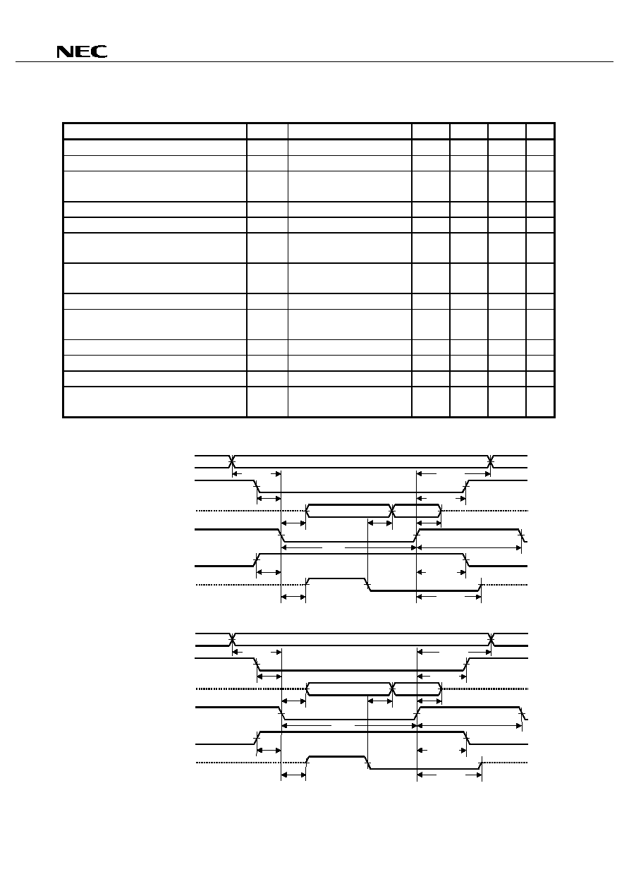
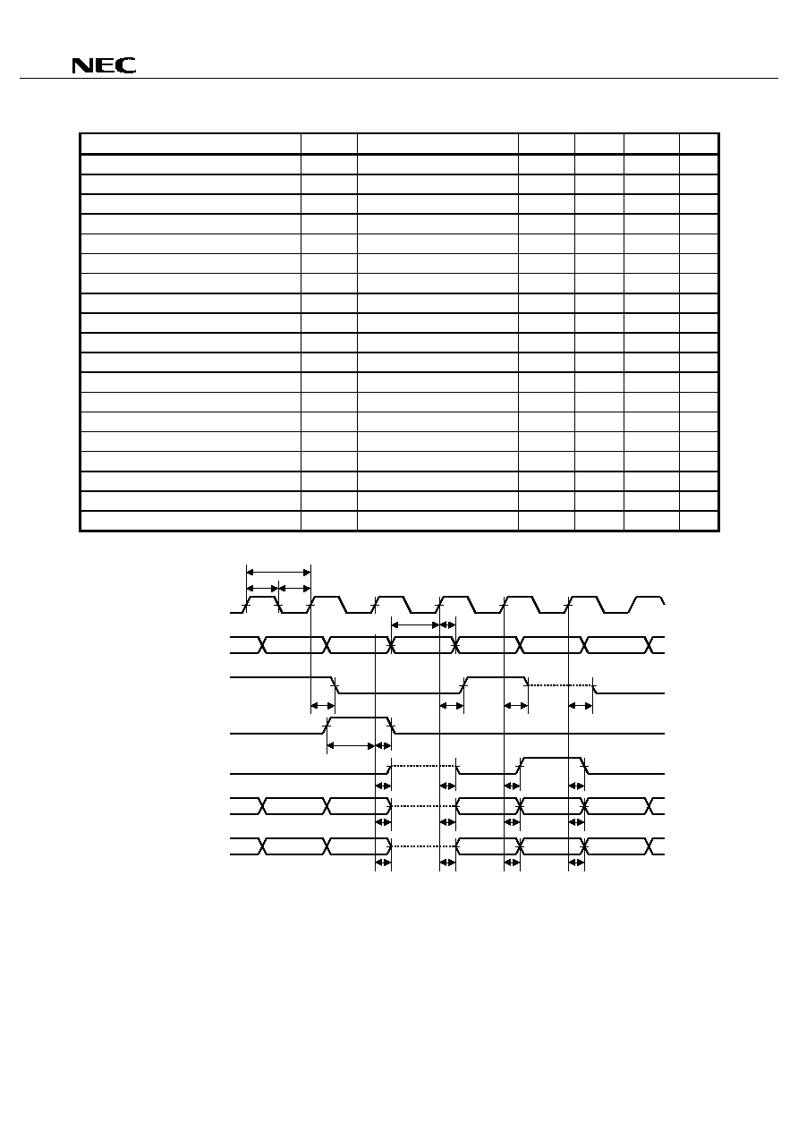
Management Interface
a) Internal Register Read
Parameter
Symbol
Conditions
MIN.
TYP.
MAX.
Unit
Address setting time (vs. DS_B
[RD_B
]) t
SADDS
10
ns
CS_B setting time (vs. DS_B
[RD_B
])
t
SCSDS
5
ns
R/W_B[WR_B] setting time
(vs. DS_B
[RD_B
])
t
SRWDS
5
ns
Address hold time (vs. DS_B
[RD_B
])
t
HADDS
4
ns
CS_B hold time (vs. DS_B
[RD_B
])
t
HCSDS
0
ns
R/W_B[WR_B] hold time
(vs. DS_B
[RD_B
])
t
HRWDS
0
ns
DS_B
[RD_B
]
ACK_B[RDY_B]
output delay
t
VAKDS
Load capacitance: 30 pF
15
ns
DS_B
[RD_B
]
data output delay
t
VDADS
Load capacitance: 30 pF
25
ns
DS_B
[RD_B
]
ACK_B[RDY_B]
float delay
t
IAKDS
Load capacitance: 30 pF
10
70
ns
DS_B
[RD_B
]
data float delay
t
IDADS
Load capacitance: 30 pF
15
70
ns
ACK_B
data output delay
t
DDAAK
Load capacitance: 30 pF
10
ns
DS_B[RD_B] pulse width
t
WDS
51.44
ns
DS_B
[RD_B
]
DS_B
[RD_B
]
recovery time
t
DSINT
51.44
ns
t
TCLK
is the cycle of the TCLK.
( i ) BMODE="0"
t
SADDS
MADD[8:0]
CS_B
MD[7:0]
DS_B /RD_B
RW_B /WR_B
ACK_B /RDY_B
t
SCSDS
t
WDS
t
VAKDS
t
DDAAK
t
HADDS
t
IDADS
t
HCSDS
t
IAKDS
t
SRWDS
t
VDADS
t
HRWDS
t
DSINT
( ii )BMODE="1"
t
DSINT
t
SADDS
t
SCSDS
t
W DS
t
VAKDS
t
DDAAK
t
HADDS
t
IDADS
t
HCSDS
t
IAKDS
t
SRW DS
t
HRW DS
t
VDADS
MADD[8:0]
CS_B
MD[7:0]
DS_B /RD_B
RW_B /WR_B
ACK_B /RDY_B
S
S
S
S
S
Data Sheet S12953EJ4V0DS00
28
µ
µ
µ
µ
PD98411
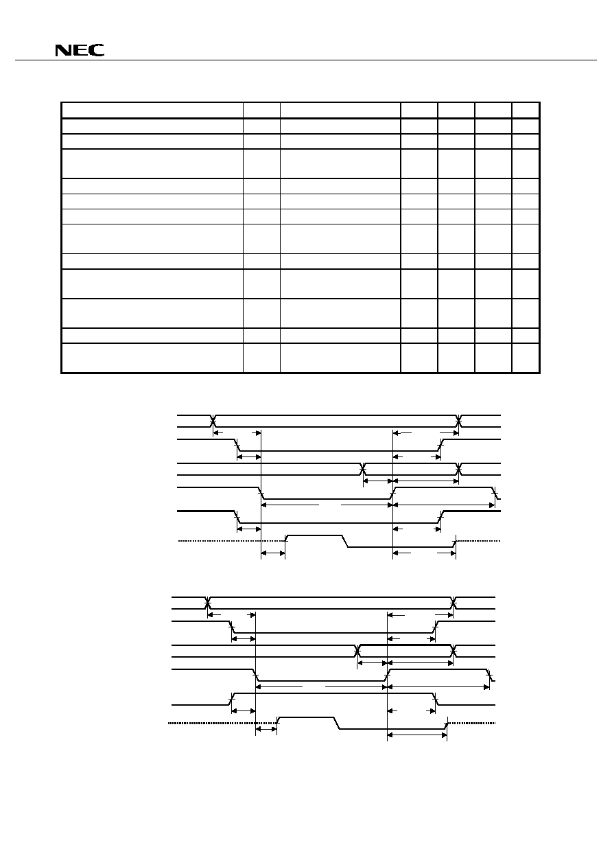
b) Internal Register Write
Parameter
Symbol
Conditions
MIN.
TYP.
MAX.
Unit
Address setting time (vs. DS_B
[RD_B
])
t
SADDS
10
ns
CS_B setting time (vs. DS_B
[WR_B
])
t
SCSDS
5
ns
R/W_B[RD_B] setting time
(vs. DS_B
[WR_B
])
t
SRWDS
5
ns
Data setting time (vs. DS_B
[WR_B
])
t
SDADS
15
ns
Address hold time (vs. DS_B
[WR_B
])
t
HADDS
4
ns
CS_B hold time (vs. DS_B
[WR_B
])
t
HCSDS
0
ns
R/W_B[RD_B] hold time
(vs. DS_B
[WR_B
])
t
HRWDS
0
ns
Data hold time (vs. DS_B
[WR_B
])
t
HDADS
4
ns
DS_B
[RD_B
]
ACK_B[RDY_B]
output delay
t
VAKDS
Load capacitance: 30 pF
15
ns
DS_B
[RD_B
]
ACK_B[RDY_B]
float delay
t
IAKDS
Load capacitance: 30 pF
10
ns
DS_B [RD_B] pulse width
t
WDS
51.44
ns
DS_B
[RD_B
]
DS_B
[RD_B
]
recovery time
t
DSINT
51.44
ns
t
TCLK
is the cycle of the TCLK.
( i )BMODE="0"
t
SRWDS
t
HDADS
MADD[8:0]
CS_B
MD[7:0]
DS_B /RD_B
RW_B /WR_B
ACK_B /RDY_B
t
SADDS
t
WDS
t
HADDS
t
HCSDS
t
VAKDS
t
IAKDS
t
SCSDS
t
HRWDS
t
SDADS
t
DSINT
( ii ) BMODE="1"
t
IAKDS
MADD[8:0]
CS_B
MD[7:0]
RW_B/WR_B
DS_B/RD_B
ACK_B/RDY_B
t
SCSDS
t
WDS
t
HADDS
t
HDADS
t
HCSDS
t
VAKDS
t
SRWDS
t
HRWDS
t
SDADS
t
SADDS
t
DSINT
S
S
Data Sheet S12953EJ4V0DS00
29
µ
µ
µ
µ
PD98411
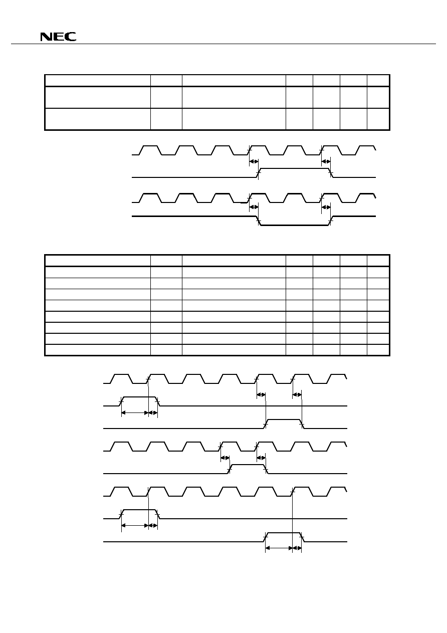
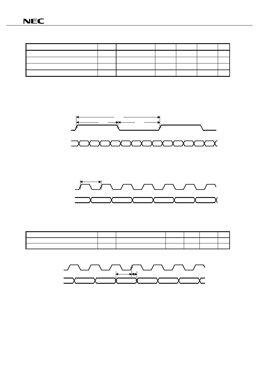
OAM Interface
Parameter
Symbol
Conditions
MIN.
TYP.
MAX.
Unit
REFCLK
PALM3[2:0] -PALM0
[2:0] delay
t
DARRL
Load capacitance: 30 pF
25
ns
REFCLK
PHINT3- PHINT 0
delay
t
DRFINT
25
ns
REFCLK
PALM3[2:0]-
PALM0[2:0]
t
DARRL
t
DARRL
REFCLK
PHINT3_B-PHINT0_B
t
DRFINT
t
DRFINT
Control Signal Interface
Parameter
Symbol
Conditions
MIN.
TYP.
MAX.
Unit
TFSS setting time (vs. TCL
)
t
STFTL
20
ns
TFSS hold time (vs. TCL
)
t
HTFTL
5
ns
TCL
TxFP delay
t
DTFTL
Load capacitance: 30 pF
25
ns
RCL
RxFP delay
t
DRFRL
Load capacitance: 30 pF
25
ns
CMD setting time (vs. REFCLK)
t
SCMRF
20
ns
CMD hold time (vs. REFCLK)
t
HCMRF
5
ns
SD setting time (vs. REFCLK)
t
SSDRF
20
ns
SD hold time (vs. REFCLK)
t
HSDRF
5
ns
t
DRFRL
t
DRFRL
TCL
t
DTFTL
t
DTFTL
t
STFTL
t
HTFTL
TFSS
TXFP
RCL
RXFP
REFCLK
t
SSDRF
t
HSDRF
t
SCMRF
t
HCMRF
CMD3-CMD0
SD3-SD0
S
S
S
Data Sheet S12953EJ4V0DS00
30
µ
µ
µ
µ
PD98411
UTOPIA Interface (transmission side)
Parameter
Symbol
Conditions
MIN.
TYP.
MAX.
Unit
TCLK cycle time
t
CYTK
20
125
ns
TCLK high-level width
t
WTKH
0.4xt
CYTK
0.6x t
CYTK
ns
TCLK low-level width
t
WTKL
0.4xt
CYTK
0.6x t
CYTK
ns
TCLK
TCLAV
delay
t
DCATK
Load capacitance: 30 pF
1
14
ns
TCLK
TCLAV output delay
t
VCATK
Load capacitance: 30 pF
1
14
ns
TCLK
TCLAV data float delay
t
ICATK
Load capacitance: 30 pF
1
20
ns
TDI[0]-TDI[7] setting time
(vs. TCLK
)
t
SDITK
4
ns
TDI[0]-TDI[7] hold time (vs. TCLK
)
t
HDITK
1
ns
TSOC setting time (vs. TCLK
)
t
SSOTK
4
ns
TSOC hold time (vs. TCLK
)
t
HSOTK
1
ns
TPR setting time (vs. TCLK
)
t
SPRTK
4
ns
TPR hold time (vs. TCLK
)
t
HPRTK
1
ns
TADD0- TADD 7 setup time
(vs. TCLK
)
t
SADTK
4
ns
TADD0- TADD7 hold time
(vs. TCLK
)
t
HADTK
1
ns
TENBL_B setting time (vs. TCLK
)
t
SENTK
4
ns
TENBL_B hold time (vs. TCLK
)
t
HENTK
1
ns
t
VCATK
t
WTKH
t
CYTK
t
WTKL
TCLK
t
SENTK
t
HENTK
t
SSOTK
t
HSOTK
TENBL2_B,
TENBL1_B
t
DCATK
t
DCATK
t
ICATK
TCLAV3-TCLAV0
t
SADTK
t
HADTK
TADD2[4:0]
TADD1[4:0]
TDI[7:0]
t
SDITK
t
HDITK
TSOC2,TSOC1
TPR2,TPR1
t
SPRTK
t
HPRTK
S
S
S
Data Sheet S12953EJ4V0DS00
31
µ
µ
µ
µ
PD98411
UTOPIA Interface (reception side)
Parameter
Symbol
Conditions
MIN.
TYP.
MAX.
Unit
RCLK cycle time
t
CYRK
20
125
ns
RCLK high-level width
t
WRKH
0.4xt
CYRK
0.6xt
CYRK
ns
RCLK low-level width
t
WRKL
0.4xt
CYRK
0.6xt
CYRK
ns
RCLK
RCLAV
delay
t
DCARK
Load capacitance: 30 pF
1
14
ns
RCLK
RCLAV output delay
t
VCARK
Load capacitance: 30 pF
1
14
ns
RCLK
RCLAV data float delay
t
ICARK
Load capacitance: 30 pF
1
20
ns
RCLK
RDO
delay
t
DDORK
Load capacitance: 30 pF
1
14
ns
RCLK
RDO output delay
t
VDORK
Load capacitance: 30 pF
1
14
ns
RCLK
RDO data float delay
t
IDORK
Load capacitance: 30 pF
1
20
ns
RCLK
RSOC
delay
t
DSORK
Load capacitance: 30 pF
1
14
ns
RCLK
RSOC output delay
t
VSORK
Load capacitance: 30 pF
1
14
ns
RCLK
RSOC data float delay
t
ISORK
Load capacitance: 30 pF
1
20
ns
RCLK
RPR
delay
t
DPRRK
Load capacitance: 30 pF
1
14
ns
RCLK
RPR output delay
t
VPRRK
Load capacitance: 30 pF
1
14
ns
RCLK
RPR data float delay
t
IPRRK
Load capacitance: 30 pF
1
20
ns
RADD setting time (vs. RCLK
)
t
SADRK
4
ns
RADD hold time (vs. RCLK
)
t
HADRK
1
ns
RENBLB setting time (vs. RCLK
)
t
SENRK
4
ns
RENBLB hold time (vs. RCLK
)
t
HENRK
1
ns
t
DSORK
t
DSORK
RCLK
RCLAV3-RCLAV0
RADD2[4:0],
RADD1[4:0]
RDO[15:0]
RSOC2,RSOC1
RENBL2_B
,
RENBL1_B
t
W RKH
t
CYRK
t
W RKL
t
DCARK
t
DCARK
t
SADRK
t
HADRK
t
ICARK
t
VCARK
t
ISORK
t
VSORK
t
SENRK
t
HENRK
t
IDORK
t
VDORK
t
DDORK
t
DDORK
RPR2,RPR1
t
IPRRK
t
VPRRK
t
DPRRK
t
DPRRK
S
S
S
S
S
S
S
S
S
S
S
S
Data Sheet S12953EJ4V0DS00
32
µ
µ
µ
µ
PD98411
PMD Interface (transmission side)
Parameter
Symbol
Conditions
MIN.
TYP.
MAX.
Unit
REFCLK cycle time
Note
t
CYRF
-20ppm
51.4403
+20ppm
ns
REFCLK high-level width
t
WRFH
0.4xt
CYRF
0.6xt
CYRF
ns
REFCLK low-level width
t
WRFL
0.4xt
CYRF
0.6xt
CYRF
ns
TFKT(C) cycle time
t
CYSF
-0.005UI
6.43
+0.005UI
ns
Note To get the transmit source clock which is a jitter below 0.01UI, the basis signal which has at least equal or
more than 40-ppm precision must be inputted.
(i) When using Clock Synthesizer
REFCLK
TDOT3-TADT0
(TDOC3-TDOC0)
t
CYFR
t
WRFH
t
WRFL
(ii) When using external serial clock
TFKT (TFKC)
t
CYSF
TDOT3-TDOT0
(TDOC3-TDOC0)
PMD Interface (reception side)
Parameter
Symbol
Conditions
MIN.
TYP.
MAX.
Unit
RDIT(C) setting time (vs. TFKT(C))
t
SDISC
When using external PLL
1.0
ns
RDIT(C) hold time (vs. TFKT(C))
t
HDISC
When using external PLL
4.0
ns
TFKT (TFKC)
RDIT3-RDIT0
(RDIC3-RDIC0)
t
SDISC
t
HDISC
Data Sheet S12953EJ4V0DS00
33
µ
µ
µ
µ
PD98411
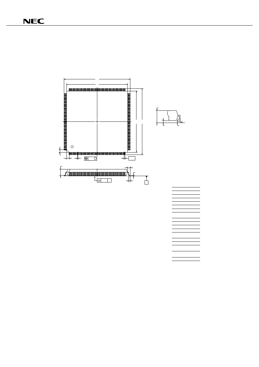
3. PACKAGE DRAWING
240-PIN PLASTIC QFP (FINE PITCH) (32x32)
ITEM
MILLIMETERS
P240GN-50-LMU, MMU, SMU-4
A
B
C
32.0
±
0.2
32.0
±
0.2
34.6
±
0.2
D
F
34.6
±
0.2
1.25
G
1.25
I
J
0.10
0.5 (T.P.)
L
0.5
±
0.2
P
3.2
±
0.1
N
0.10
Q
0.4
±
0.1
S
3.8 MAX.
R
3
+
7
-
3
H
0.22
+
0.05
-
0.04
M
0.17
+
0.03
-
0.07
N
detail of lead end
I
J
F
G
H
Q
R
P
K
M
L
M
S
NOTE
Each lead centerline is located within 0.10 mm of
its true position (T.P.) at maximum material condition.
180
121
120
181
61
240
1
60
S
A
B
C
D
S
K
1.3
±
0.2

Data Sheet S12953EJ4V0DS00
34
µ
µ
µ
µ
PD98411
4. RECOMMENDED SOLDERING CONDITIONS
The conditions listed below shall be met when soldering this product.
For more details, refer to our document "Semiconductor Device Mounting Technology Manual (C10535E)".
Please consult with our sales offices in case other soldering process is used, or in case the soldering is done
under different conditions.
Surface-mount devices
∑
µ
PD98411GN-MMU: 240-pin plastic QFP (fine pitch) (32 x 32 mm)
Soldering process
Soldering conditions
Symbol
Infrared ray reflow
Peak package's surface temperature :235
∞
C or below,
Reflow time : 30 seconds or below (210
∞
C or higher),
Number of reflow profess : 1,
Exposure limit
Note
:3 days (36 hours pre-backing is required at 125C
∞
afterwards)
IR35-363-1
Partial heating method
Terminal temperature :300
∞
C or below,
Flow time : 3 seconds or below (Per one side of the device).
--
Note Exposure limit before soldering after dry-pack package is opened.
Storage conditions: 25
∞
C and relative humidity at 65% or less.

Data Sheet S12953EJ4V0DS00
35
µ
µ
µ
µ
PD98411
NOTES FOR CMOS DEVICES
1
PRECAUTION AGAINST ESD FOR SEMICONDUCTORS
Note: Strong electric field, when exposed to a MOS device, can cause destruction
of the gate oxide and ultimately degrade the device operation. Steps must
be taken to stop generation of static electricity as much as possible, and
quickly dissipate it once, when it has occurred. Environmental control must
be adequate. When it is dry, humidifier should be used. It is recommended
to avoid using insulators that easily build static electricity. Semiconductor
devices must be stored and transported in an anti-static container, static
shielding bag or conductive material. All test and measurement tools
including work bench and floor should be grounded. The operator should
be grounded using wrist strap. Semiconductor devices must not be touched
with bare hands. Similar precautions need to be taken for PW boards with
semiconductor devices on it.
2
HANDLING OF UNUSED INPUT PINS FOR CMOS
Note: No connection for CMOS device inputs can be cause of malfunction. If no
connection is provided to the input pins, it is possible that an internal input
level may be generated due to noise, etc., hence causing malfunction. CMOS
devices behave differently than Bipolar or NMOS devices. Input levels of
CMOS devices must be fixed high or low by using a pull-up or pull-down
circuitry. Each unused pin should be connected to V
DD
or GND with a
resistor, if it is considered to have a possibility of being an output pin. All
handling related to the unused pins must be judged device by device and
related specifications governing the devices.
3
STATUS BEFORE INITIALIZATION OF MOS DEVICES
Note: Power-on does not necessarily define initial status of MOS device. Production
process of MOS does not define the initial operation status of the device.
Immediately after the power source is turned ON, the devices with reset
function have not yet been initialized. Hence, power-on does not guarantee
out-pin levels, I/O settings or contents of registers. Device is not initialized
until the reset signal is received. Reset operation must be executed imme-
diately after power-on for devices having reset function.

µ
µ
µ
µ
PD98411
NEASCOT-P40 is a trademark of NEC corporation.
The export of this product from Japan is prohibited without governmental license. To export or re-export this product from
a country other than Japan may also be prohibited without a license from that country. Please call an NEC sales
representative.
∑
The information in this document is subject to change without notice. Before using this document, please
confirm that this is the latest version.
∑
No part of this document may be copied or reproduced in any form or by any means without the prior written
consent of NEC Corporation. NEC Corporation assumes no responsibility for any errors which may appear in
this document.
∑
NEC Corporation does not assume any liability for infringement of patents, copyrights or other intellectual property
rights of third parties by or arising from use of a device described herein or any other liability arising from use
of such device. No license, either express, implied or otherwise, is granted under any patents, copyrights or other
intellectual property rights of NEC Corporation or others.
∑
Descriptions of circuits, software, and other related information in this document are provided for illustrative
purposes in semiconductor product operation and application examples. The incorporation of these circuits,
software, and information in the design of the customer's equipment shall be done under the full responsibility
of the customer. NEC Corporation assumes no responsibility for any losses incurred by the customer or third
parties arising from the use of these circuits, software, and information.
∑
While NEC Corporation has been making continuous effort to enhance the reliability of its semiconductor devices,
the possibility of defects cannot be eliminated entirely. To minimize risks of damage or injury to persons or
property arising from a defect in an NEC semiconductor device, customers must incorporate sufficient safety
measures in its design, such as redundancy, fire-containment, and anti-failure features.
∑
NEC devices are classified into the following three quality grades:
"Standard", "Special", and "Specific". The Specific quality grade applies only to devices developed based on a
customer designated "quality assurance program" for a specific application. The recommended applications of
a device depend on its quality grade, as indicated below. Customers must check the quality grade of each device
before using it in a particular application.
Standard: Computers, office equipment, communications equipment, test and measurement equipment,
audio and visual equipment, home electronic appliances, machine tools, personal electronic
equipment and industrial robots
Special: Transportation equipment (automobiles, trains, ships, etc.), traffic control systems, anti-disaster
systems, anti-crime systems, safety equipment and medical equipment (not specifically designed
for life support)
Specific: Aircraft, aerospace equipment, submersible repeaters, nuclear reactor control systems, life
support systems or medical equipment for life support, etc.
The quality grade of NEC devices is "Standard" unless otherwise specified in NEC's Data Sheets or Data Books.
If customers intend to use NEC devices for applications other than those specified for Standard quality grade,
they should contact an NEC sales representative in advance.
M7 98. 8