 | –≠–ª–µ–∫—Ç—Ä–æ–Ω–Ω—ã–π –∫–æ–º–ø–æ–Ω–µ–Ω—Ç: UPG133G | –°–∫–∞—á–∞—Ç—å:  PDF PDF  ZIP ZIP |
©
1996
DATA SHEET
GaAs INTEGRATED CIRCUIT
µµ
µµµ
PG133G
DESCRIPTION
UPG133G is an L-Band SPDT (Single Pole Double Throw) GaAs FET switch which was developed for digital cellular
or cordless telephone application.
The device can operate from 100 MHz to 2.5 GHz, having the low insertion loss.
It housed in an original 8 pin SSOP that is smaller than usual 8 pin SOP and easy to install and contributes to
miniaturizing the system.
It can be used in wide-band switching applications.
FEATURES
∑
Maximum transmission power :
0.25 W (typ.)
∑
Low insertion loss
:
0.6 dB (typ.) at f = 2 GHz
∑
High switching speed
:
10 ns
∑
Small package
:
8 pins SSOP
APPLICATION
∑
Digital cordless telephone
:
PHS, PCS, DECT etc.
∑
Digital hand-held cellular phone, WLAN
ORDERING INFORMATION
PART NUMBER
PACKAGE
PACKING FORM
µ
PG133G-E1
8 pin plastic SSOP
Carrier tape width 12 mm.
QTY 2kp/Reel.
For evaluation sample order, please contact your local NEC sales office.
ABSOLUTE MAXIMUM RATINGS (T
A
= 25 ∞C)
Control Voltage
V
CONT
≠6 to +0.6
V
Input Power
P
in
25
dBm
Total Power Dissipation
P
tot
0.2
W
Operating Case Temperature
T
opt
≠65 to +90
∞C
Storage Temperature
T
stg
≠65 to +150
∞C
CAUTION:
The IC must be handled with care to prevent static discharge because its circuit is composed
of GaAs MES FET.
L-BAND SPDT SWITCH
Document No. P10733EJ2V0DS00 (2nd edition)
Date Published April 1996 P
Printed in Japan
µµ
µµ
µ
PG133G
2
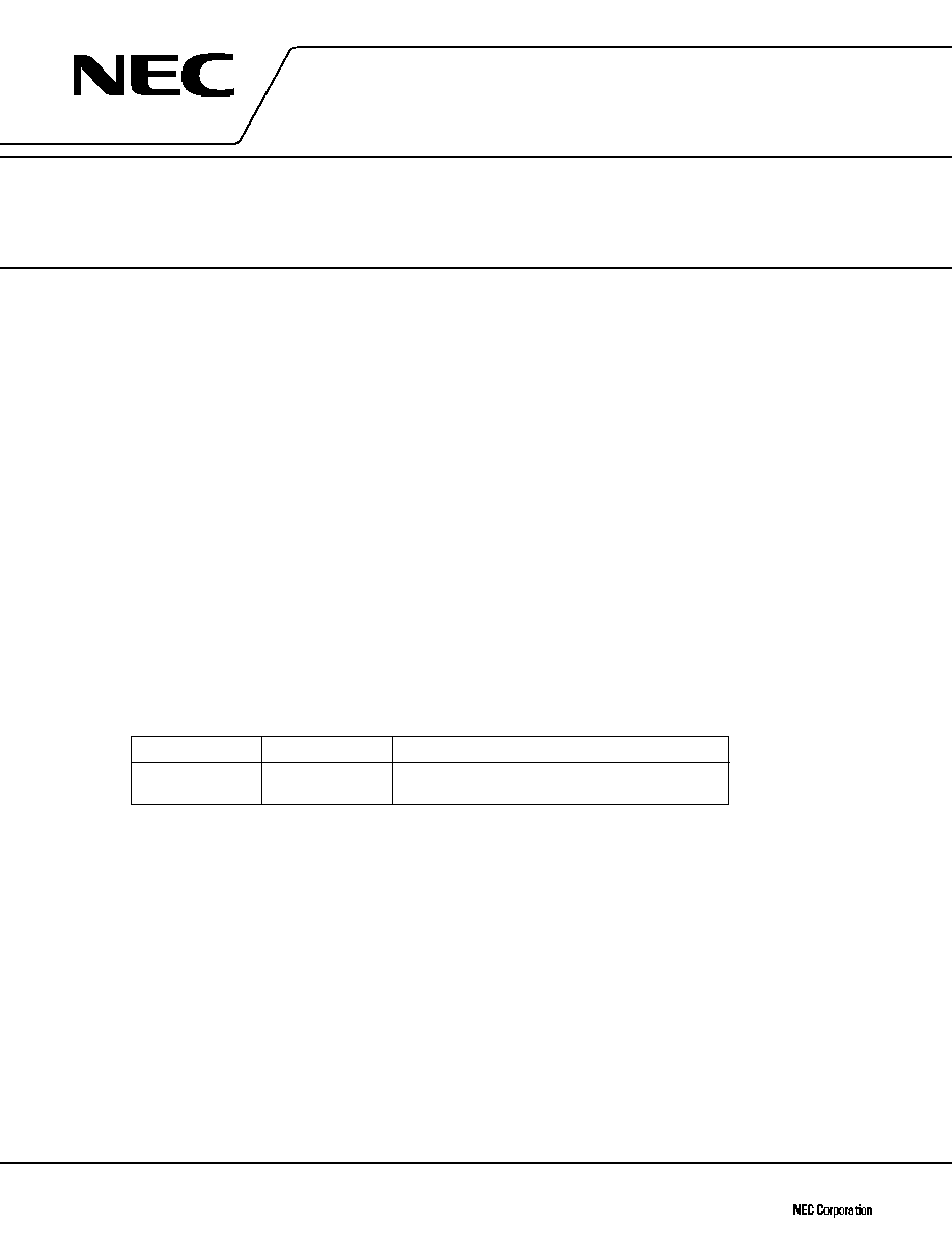
PIN CONNECTION DIAGRAM (Top View)
SPDT SWITCH IC SERIES PRODUCTS
PART
Pin (1dB)
LINS
ISL
VCONT
PACKAGE
APPLICATIONS
NUMBER
(dBm)
(dB)
(dB)
(V)
µ
PG130GR
+34
0.5 @1G
32 @1G
≠5/0
8 pin SOP
PDC, IS-136, PHS
µ
PG131GR
+30
0.6 @2G
23 @2G
≠4/0
(225 mil)
PHS, PCS, WLAN
µ
PG130G
+34
0.5 @1G
32 @1G
≠5/0
8 pin SSOP
PDC, IS-136, PHS
µ
PG131G
+30
0.6 @2G
23 @2G
≠4/0
(175 mil)
PHS, PCS, WLAN
µ
PG132G
+30
0.6 @2G
22 @2G
+3/0
PHS, PCS, WLAN
µ
PG133G
+25
0.6 @2G
20 @2G
≠3/0
DIVERSITY etc
Remark: As for detail information of series products, please refer to each data sheet.
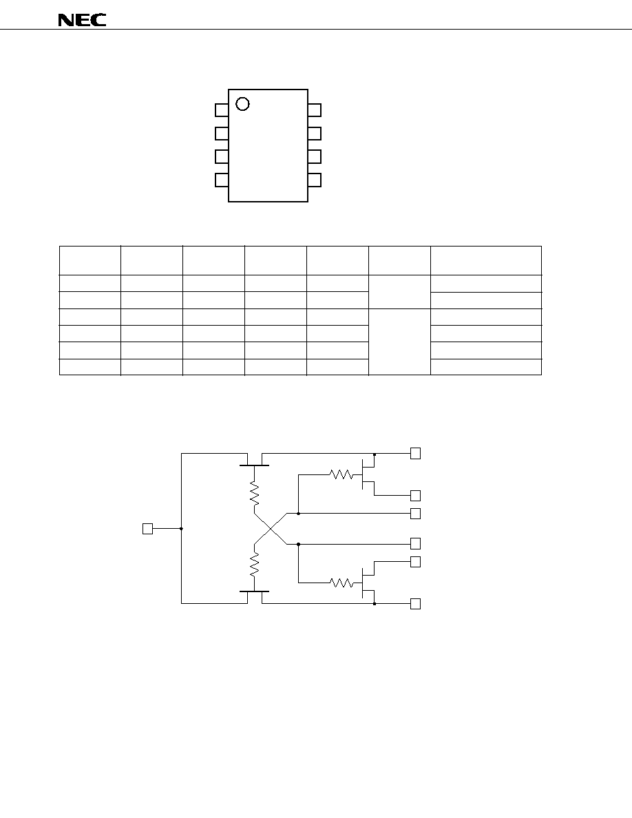
EQUIVALENT CIRCUIT
IN
OUT1
GND
VCONT1
VCONT2
GND
OUT2
1
2
3
4
8
7
6
5
1. V
CONT2
2. OUT2
3. GND
4. GND
5. IN
6. GND
7. OUT1
8. V
CONT1
µµ
µµ
µ
PG133G
3
RECOMMENDED OPERATING CONDITIONS
PARAMETER
SYMBOL
MIN.
TYP.
MAX.
UNIT
Control Voltage (ON)
V
CONT
≠0.2
0
+0.2
V
Control Voltage (OFF)
V
CONT
≠5.0
≠3.0
≠2.7
V
Input Power Level
P
in
21
24
dBm
ELECTRICAL CHARACTERISTICS (T
A
= 25 ∞C)
CHARACTERISTICS
SYMBOL
MIN.
TYP.
MAX.
UNIT
TEST CONDITION
Insertion Loss
L
INS
0.6
1.0
dB
0.8
Note1
f = 2.5 GHz
Isolation
ISL
20
dB
20
Note1
f = 2.5 GHz
Input Return Loss
RL
in
11
20
dB
f = 100 MHz to 2 GHz
Output Return Loss
RL
out
11
20
dB
V
CONT1
= 0 V
Input Power at 1dB
P
in
(1dB)
Note2
21
25
dBm
V
CONT2
= ≠3 V
Compression Point
or
Switching Speed
t
sw
10
ns
V
CONT1
= ≠3 V
Control Current
I
CONT
50
µ
A
V
CONT2
= 0 V
Notes 1: Characteristic for reference at 2.0 to 2.5 GHz
2: P
in
(1dB) is measured the input power level when the insertion loss increase more 1dB than that of linear
range.
All other characteristics are measured in linear range.
NOTE ON CORRECT USE
∑
Insertion loss and isolation of the IN-OUT2 is better than that of IN-OUT1, because No. 7 pin (OUT1) is placed
to same side of No. 5 pin (IN).
∑
The distance between IC's GND pins and ground pattern of substrate should be as shorter as possible to avoid
parasitic parameters.
µµ
µµ
µ
PG133G
4
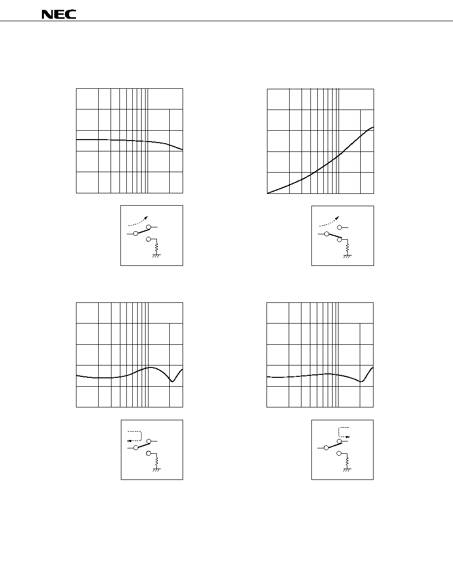
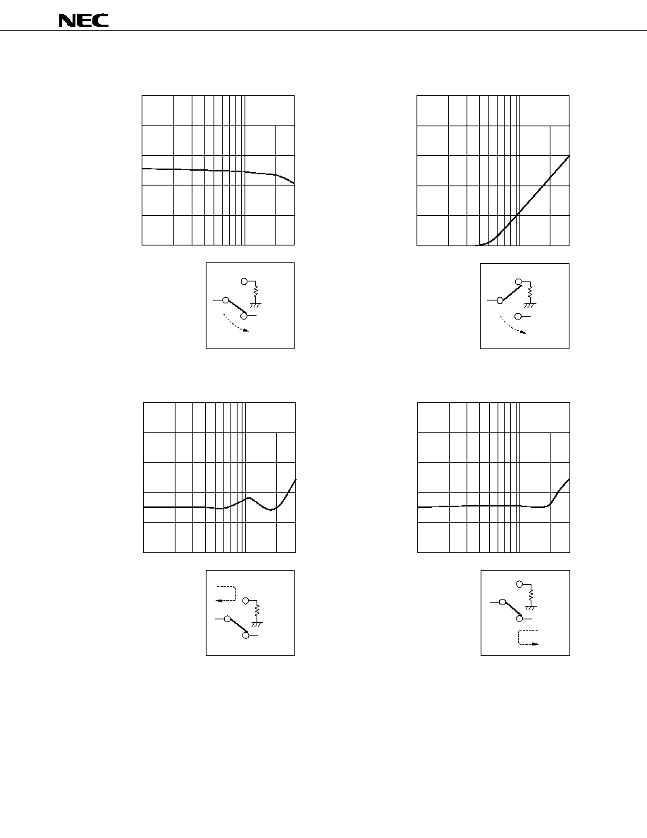
TYPICAL CHARACTERISTICS (T
A
= 25 ∞C)
Note This data is including loss of the test fixture.
+ 2.0
+ 1.0
0
≠ 1.0
≠ 2.0
≠ 3.0
V
CONT1
= ≠3 V
V
CONT2
= 0 V
P
in
= 0 dBm
100 M 200 M
500 M
1 G
2 G 3 G
f - Frequency - Hz
L
INS
IN
OUT1
OUT2
50
L
INS
- Insertion Loss - dB
IN-OUT1 INSERTION LOSS vs. FREQUENCY
0
≠10
≠20
≠ 30
≠ 40
≠ 50
V
CONT1
= 0 V
V
CONT2
= ≠3 V
P
in
= 0 dBm
100 M 200 M
500 M
1 G
2 G 3 G
f - Frequency - Hz
ISL
IN
OUT1
OUT2
50
ISL - Isolation - dB
IN-OUT1 ISOLATION vs. FREQUENCY
+ 10
0
≠10
≠ 20
≠ 30
≠ 40
V
CONT1
= ≠3 V
V
CONT2
= 0 V
P
in
= 0 dBm
100 M 200 M
500 M
1 G
2 G 3 G
f - Frequency - Hz
RL
in
IN
OUT1
OUT2
50
RL
in
- Input Return Loss - dB
IN-OUT1 INPUT RETURN LOSS vs. FREQUENCY
+ 10
0
≠10
≠ 20
≠ 30
≠ 40
100 M 200 M
500 M
1 G
2 G 3 G
f - Frequency - Hz
RL
OUT
IN
OUT1
OUT2
50
RL
out
- Output Return Loss - dB
IN-OUT1 OUTPUT RETURN LOSS vs. FREQUENCY
V
CONT1
= ≠3 V
V
CONT2
= 0 V
P
in
= 0 dBm
µµ
µµ
µ
PG133G
5
+ 2.0
+ 1.0
0
≠ 1.0
≠ 2.0
≠ 3.0
V
CONT1
= ≠3 V
V
CONT2
= 0 V
P
in
= 0 dBm
100 M 200 M
500 M
1 G
2 G 3 G
f - Frequency - Hz
L
INS
IN
OUT1
OUT2
50
L
INS
- Insertion Loss - dB
IN-OUT2 INSERTION LOSS vs. FREQUENCY
0
≠10
≠20
≠ 30
≠ 40
≠ 50
V
CONT1
= 0 V
V
CONT2
= ≠3 V
P
in
= 0 dBm
100 M 200 M
500 M
1 G
2 G 3 G
f - Frequency - Hz
ISL - Isolation - dB
IN-OUT2 ISOLATION vs. FREQUENCY
+ 10
0
≠10
≠ 20
≠ 30
≠ 40
100 M 200 M
500 M
1 G
2 G 3 G
f - Frequency - Hz
RL
in
IN
OUT1
OUT2
50
RL
in
- Input Return Loss - dB
IN-OUT2 INPUT RETURN LOSS vs. FREQUENCY
+ 10
0
≠10
≠ 20
≠ 30
≠ 40
100 M 200 M
500 M
1 G
2 G 3 G
f - Frequency - Hz
RL
OUT
IN
OUT1
OUT2
50
RL
out
- Output Return Loss - dB
IN-OUT2 OUTPUT RETURN LOSS vs. FREQUENCY
ISL
IN
OUT1
OUT2
50
V
CONT1
= 0 V
V
CONT2
= ≠3 V
P
in
= 0 dBm
V
CONT1
= 0 V
V
CONT2
= ≠3 V
P
in
= 0 dBm
µµ
µµ
µ
PG133G
6
28
26
24
22
20
P
in
- Input Power - dBm
IN
OUT1
OUT2
50
P
out
- Output Power - dB
IN-OUT2 P
in
vs. P
out
V
CONT1
= 0 V
V
CONT2
= ≠3 V
f = 1.9 GHz
18
30
18
22 24 26 28 30
20
V
CONT1
= 0 V
V
CONT2
= ≠3 V
f = 2 GHz
P
in
= +20 dBm
Signal input (CW)
1.0
0.8
0.6
L
INS
(dB)
≠50
≠60
≠70
2f
o
, 3f
o
Harmonics (dBC)
3f
o
2f
o
≠100
≠50
0
+50
+100
INSERTION LOSS, 2f
o
, 3f
o
vs.
AMBIENT TEMPERATURE
V
CONT1
= 0 V
V
CONT2
= ≠3 V
f = 2GHz
Non-modulated
signal input (CW)
T
A
= ≠50 ∞C
T
A
= +25 ∞C
T
A
= +90 ∞C
30
25
20
15
15
20
25
30
P
in
(dBm)
P
out
(dBm)
INPUT POWER vs. OUTPUT POWER
T
A
(∞C)
L
INS
µµ
µµ
µ
PG133G
7
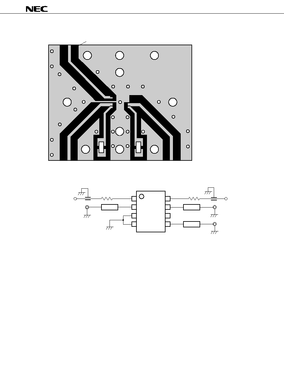
TEST BOARD
R
R
IN
0.9 mm width.
0.4 mm thickness
teflon glass
R = 50
NEC
G130/131
OUT1
OUT2
V
CONT1
V
CONT2
Using the same board that of
PG130/131G
µ
TEST CIRCUIT
1
2
3
4
8
7
6
5
50
V
CONT2
= 0 V/≠3 V
1 000 pF
OUT2
Z
O
= 50
50
Z
O
= 50
Z
O
= 50
OUT1
1 000 pF
V
CONT1
= ≠3 V/0 V
IN
µµ
µµ
µ
PG133G
8
µµ
µµ
µ
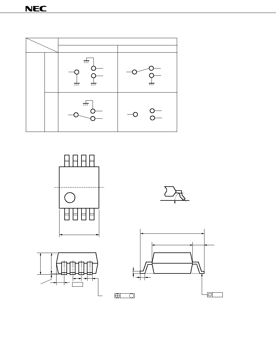
PG133G TRUTH TABLE OF SWITCHING BY CONDITION OF CONTROL VOLTAGE
V
CONT1
0 V
≠3 V
0 V
V
CONT2
≠3 V
8-PIN PLASTIC SHRINK SOP (175 mil) (Unit mm)
5
8
4
1
3.0 MAX.
3∞
+7 ≠3
1.8 MAX.
1.5 ±0.1
0.1 ±0.1
0.575 MAX.
0.65
0.10
0.3
+0.10
≠0.05
M
0.15
+0.10
≠0.05
0.5 ±0.2
3.2 ±0.1
0.15
4.94 ±0.2
0.87 ±0.2
Detail of lead end
IN
OUT1
OUT2
OUT2
IN
OUT1
IN
OUT1
OUT2
OUT2
IN
OUT1
µµ
µµ
µ
PG133G
9
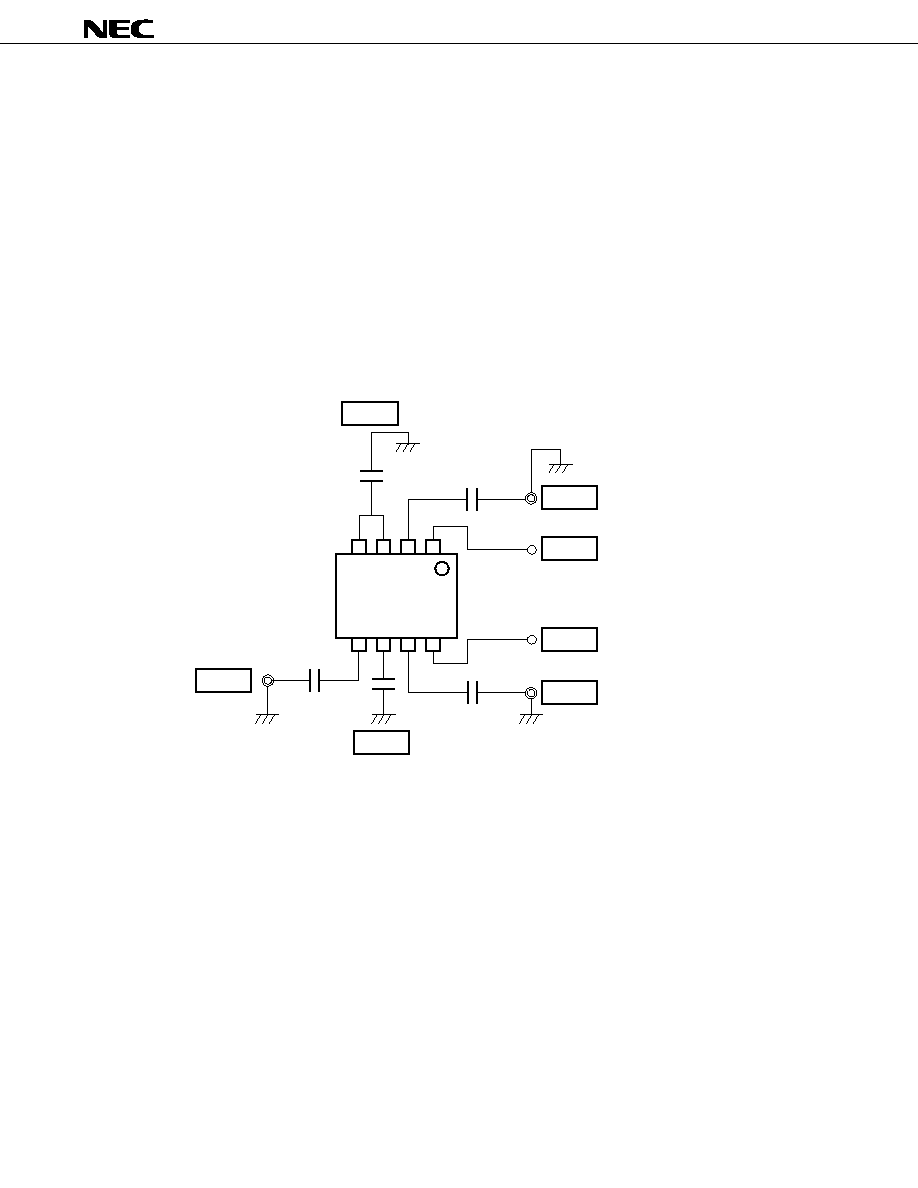
Floating the
µµ
µµ
µ
PG133G
It is possible to use the
µ
PG133G with only a single +3 V supply by employing a technique known as "floating".
When the IC is floated using a +3 V supply, the voltage levels used to control the switch are elevated above ground
by +3 V.
When the
µ
PG133G is floated it is necessary to use DC blocking (C2, C3, C5) and grounding (C1, C4) capacitors.
This enables the IC to isolated so that +3 V can be applied to RF line. The value for DC blocking capacitors should
be chosen to accommodate the frequency of operation. Grounding capacitors are required to float the IC above
ground. The value for grounding capacitor should be chosen to accommodate the frequency of operation.
It is not recommended to float the
µ
PG133G for wide band application.
(Floating the
µ
PG133G with +3 V/0 V supply at 2 GHz-band, BW
50 MHz)
C1
C2
PIN CONNECTIONS
1
4
8
5
V
CONT2
V
CONT1
OUT2
GND
C5
OUT1
IN
C4
C3
GND
1. V
CONT2
2. OUT2
3. GND
4. GND
5. IN
6. GND
7. OUT1
8. V
CONT1
C1, C4 = 10 pF below :
Grounding capacitor
C2, C3, C5 = 100 pF :
DC blocking capacitor
The distance between grounding capacitor and IC's GND pins, grounding capacitor and ground of the
substrate should be as shorter as possible to avoid the parasitic parameters. IC's GND pin, No. 3, No. 4 and No.
6 are connected inside of the IC.
µµ
µµ
µ
PG133G
10
RECOMMENDED SOLDERING CONDITIONS
This product should be soldered in the following recommended conditions. Other soldering methods and conditions
than the recommended conditions are to be consulted with our sales representatives.
[
µµ
µµ
µ
PG133G]
Soldering process
Soldering conditions
Recommended condition
symbol
Infrared ray reflow
Package peak temperature: 230 ∞C
IR30-00-2
Hour: within 30 s. (more than 210 ∞C)
Time: 2 time, Limited days: no.
Note
VPS
Package peak temperature: 215 ∞C
VP15-00-2
Hour: within 40 s. (more than 200 ∞C),
Time: 2 time, Limited days: no.
Note
Wave Soldering
Soldering tub temperature: less than 260 ∞C, Hour: within 10 s.
WS60-00-1
Time: 1 time, Limited days: no.
Note
Pin part heating
Pin area temperature: less than 300 ∞C, Hour: within 10 s.
Limited days: no.
Note
Note It is storage days after opening a dry pack, the storage conditions are 25 ∞C, less than 65 %, RH.
Caution The combined use of soldering method is to be avoided (However, except the pin area heating
method).

µ
PG133G
11
[MEMO]
2
µµ
µµ
µ
PG133G
No part of this document may be copied or reproduced in any form or by any means without the prior written
consent of NEC Corporation. NEC Corporation assumes no responsibility for any errors which may appear in this
document.
NEC Corporation does not assume any liability for infringement of patents, copyrights or other intellectual
property rights of third parties by or arising from use of a device described herein or any other liability arising
from use of such device. No license, either express, implied or otherwise, is granted under any patents,
copyrights or other intellectual property rights of NEC Corporation or others.
While NEC Corporation has been making continuous effort to enhance the reliability of its semiconductor devices,
the possibility of defects cannot be eliminated entirely. To minimize risks of damage or injury to persons or
property arising from a defect in an NEC semiconductor device, customer must incorporate sufficient safety
measures in its design, such as redundancy, fire-containment, and anti-failure features.
NEC devices are classified into the following three quality grades:
"Standard", "Special", and "Specific". The Specific quality grade applies only to devices developed based on
a customer designated "quality assurance program" for a specific application. The recommended applications
of a device depend on its quality grade, as indicated below. Customers must check the quality grade of each
device before using it in a particular application.
Standard: Computers, office equipment, communications equipment, test and measurement equipment,
audio and visual equipment, home electronic appliances, machine tools, personal electronic
equipment and industrial robots
Special:
Transportation equipment (automobiles, trains, ships, etc.), traffic control systems, anti-disaster
systems, anti-crime systems, safety equipment and medical equipment (not specifically designed
for life support)
Specific: Aircrafts, aerospace equipment, submersible repeaters, nuclear reactor control systems, life
support systems or medical equipment for life support, etc.
The quality grade of NEC devices in "Standard" unless otherwise specified in NEC's Data Sheets or Data Books.
If customers intend to use NEC devices for applications other than those specified for Standard quality grade,
they should contact NEC Sales Representative in advance.
Anti-radioactive design is not implemented in this product.
M4 94.11
Caution
The Great Care must be taken in dealing with the devices in this guide.
The reason is that the material of the devices is GaAs (Gallium Arsenide), which is
designated as harmful substance according to the Japanese law concerned.
Keep the law concerned and so on, especially in case of removal.