 | –≠–ª–µ–∫—Ç—Ä–æ–Ω–Ω—ã–π –∫–æ–º–ø–æ–Ω–µ–Ω—Ç: UPG139GV | –°–∫–∞—á–∞—Ç—å:  PDF PDF  ZIP ZIP |
The information in this document is subject to change without notice.
GaAs INTEGRATED CIRCUIT
µ
µ
µ
µ
PG139GV
1998
©
Document No. P13144EJ2V0DS00 (2nd edition)
Date Published July 1998 N CP(K)
Printed in Japan
L-BAND DPDT MMIC SWITCH
DATA SHEET
The mark shows major revised points.
DESCRIPTION
The
µ
PG139GV is L-Band Double Pole, Double Throw (DPDT) switch developed for digital cellular or cordless
telephone and PCS applications. This device feature low insertion loss, high handling power with low voltage
operation. It is housed in a very small 8-pin plastic SSOP package available on tape-and-reel and easy to install and
contributes to miniaturizing the systems.
FEATURES
{
High-Power Switching : Pin(1 dB) = +34 dBm typ. @ANT1, 2-TX, V
DD
= 3.0 V, V
CONT
= 3.6 V, f = 100 M to 2 GHz
Pin(0.5 dB) = +36 dBm typ. @ANT1, 2-TX, V
DD
= 5.0 V, V
CONT
= 5.0 V, f = 100 M to 2 GHz
{
Low Insertion Loss
: Lins1 = 0.70 dB typ. @ANT1, 2-TX, V
DD
= 3.0 V, V
CONT
= 3.6 V, f = 1 GHz
Lins4 = 0.85 dB typ. @ANT1, 2-RX, V
DD
= 3.0 V, V
CONT
= 3.6 V, f = 1 GHz
{
Small 8-pin SSOP (175 mil) Package
APPLICATION
{
Digital Cellular: PDC, GSM, IS-95, IS-136 etc.
{
PCS, PHS Base station etc.
ORDERING INFORMATION
Part Number
Package
Packing Form
µ
PG139GV-E1
8-pin SSOP (175 mil)
Carrier tape width is 12 mm, Quantity is 2 kpcs per reel.
Remark
For sample order, please contact your local NEC sales office. (Part number for sample order:
µ
PG139GV)
Caution
The IC must be handled with care to prevent static discharge because its circuit composed of GaAs
MESFET.
2
µ
µ
µ
µ
PG139GV
ABSOLUTE MAXIMUM RATINGS (T
A
= 25∞C)
Parameters
Symbol
Conditions
Ratings
Unit
Supply Voltage
V
DD
V
CONT
(H)
V
Control Voltage 1, 2
V
CONT1, 2
≠6.0 to +6.0
Note1
V
Input Power (ANT1, 2-TX)
P
in
V
CONT
= +5 V/0 V
+36
dBm
Input Power (ANT1, 2-RX)
P
in
V
CONT
= +5 V/0 V
+34
dBm
Input Power (ANT1, 2-TX)
P
in
V
CONT
= +3 V/0 V
+34
dBm
Input Power (ANT1, 2-RX)
P
in
V
CONT
= +3 V/0 V
+32
dBm
Total Power Dissipation
P
tot
0.7
Note 2
W
Operating Temperature
T
A
≠50 to +80
∞C
Storage Temperature
T
stg
≠65 to +150
∞C
Notes 1. 2.7 V
| V
CONT1
≠ V
CONT2
|
6.0
2. Mounted on a 50
◊
50
◊
1.6 mm double copper clad epoxy glass PWB, T
A
= +85 ∞C
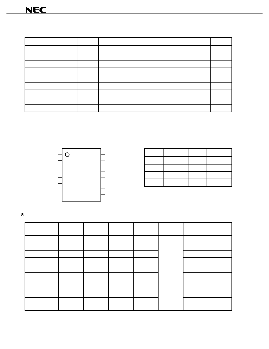
PIN CONNECTION (Top View)
Pin No.
Connection
Pin No.
Connection
1
TX
5
RX
2
V
DD
6
V
CONT1
3
V
CONT2
7
GND
4
ANT2
8
ANT1
SWITCH IC SERIES PRODUCTS
Part Number
Pin (1 dB)
(dBm)
LINS (dB)
ISL (dB)
V
CONT
(V)
Package
Application
µ
PG130G
+34
0.5@1G
32@1G
≠5/0
8-pin SSOP
PDC, IS-136, PHS
µ
PG131G
+30
0.6@2G
23@2G
≠4/0
(175 mil)
PHS, PCS, WLAN
µ
PG132G
+30
0.6@2G
22@2G
+3/0
PHS, PCS, WLAN
µ
PG133G
+25
0.6@2G
20@2G
≠3/0
DIVERSITY, VCO
µ
PG137GV
+34
0.55@1G
25@2G
+3/0
PDC, GSM, IS-136
µ
PG138GV
+34
+37
0.55@1G
30@1G
≠3/0
≠5/0
PDC, GSM, IS-136
µ
PG139GV
(ANT1, 2-TX)
+34
1.20@2G
12.5@2G
+3.6/0
PDC, IS-95, IS-136
µ
PG139GV
(ANT1, 2-RX)
+30
1.00@2G
14@2G
+3.6/0
PDC, IS-95, IS-136
Remark
As for detail information of series products, please refer to each data sheet.
1
2
3
4
8
7
6
5
G139
3
µ
µ
µ
µ
PG139GV
RECOMMENDED OPERATING CONDITIONS (T
A
= 25∞C)
Parameters
Symbol
MIN.
TYP.
MAX.
Unit
Control Voltage (High)
V
CONT(H)
+2.7
+3.6
+5.3
V
Control Voltage (Low)
V
CONT(L)
≠0.2
0
+0.2
V
Supply Voltage
V
DD
V
CONT(H)
≠ 0.7
V
CONT(H)
≠ 0.6
V
CONT(H)
≠ 0.5
V
Input Power (ANT1, 2-TX, V
CONT
= +5 V)
P
in
+36
dBm
Input Power (ANT1, 2-RX, V
CONT
= +5 V)
P
in
+33
dBm
Input Power (ANT1, 2-TX, V
CONT
= +3 V)
P
in
+33
dBm
Input Power (ANT1, 2-RX, V
CONT
= +3 V)
P
in
+31
dBm
ELECTRICAL CHARACTERISTICS
(Unless otherwise specified, T
A
= 25∞C, V
CONT
= +3.6 V/0 V, V
DD
= +3.0 V, ZS = ZL = 50
)
Parameters
Symbol
Test Conditions
MIN.
TYP.
MAX.
Unit
Insertion Loss 1
L
INS
1
ANT1, 2-TX, f = 100 M to 1 GHz
0.70
0.85
dB
Insertion Loss 2
L
INS
2
ANT1, 2-TX, f = 1.5 GHz
0.90
1.00
dB
Insertion Loss 3
L
INS
3
ANT1, 2-TX, f = 2 GHz
1.20
1.30
dB
Insertion Loss 4
L
INS
4
ANT1, 2-RX, f = 100 M to 1 GHz
0.85
0.95
dB
Insertion Loss 5
L
INS
5
ANT1, 2-RX, f = 1.5 GHz
1.05
1.15
dB
Insertion Loss 6
L
INS
6
ANT1, 2-RX, f = 2 GHz
1.30
1.40
dB
Isolation 1
ISL1
ANT1, 2-TX, f = 100 M to 1.5 GHz
13.5
15.5
dB
Isolation 2
ISL2
ANT1, 2-TX, f = 2 GHz
10.5
12.5
dB
Isolation 3
ISL3
ANT1, 2-RX, f = 100 M to 1.5 GHz
13.5
15.5
dB
Isolation 4
ISL4
ANT1, 2-RX, f = 2 GHz
10.5
12.5
dB
Input Return Loss
RL
in
f = 100 M to 2 GHz
11
15
dB
Output Return Loss
RL
out
f = 100 M to 2 GHz
11
15
dB
1 dB Compression Point
Note
P
in(1 dB)
1
ANT1, 2-TX, f = 100 M to 2 GHz
+32
+34
dBm
1 dB Compression Point
Note
P
in(1 dB)
2
ANT1, 2-RX, f = 100 M to 2 GHz
+27
+30
dBm
Input Power at 0.5 dB
Compression Point
Note
P
in(0.5 dB)
3
ANT1, 2-TX, f = 100 M to 2 GHz
V
CONT
= +5 V/0 V V
DD
= +5.0 V
+36
dBm
Input Power at 0.5 dB
Compression Point
Note
P
in(0.5 dB)
4
ANT1, 2-RX, f = 100 M to 2 GHz
V
CONT
= +5 V/0 V V
DD
= +5.0 V
+33
dBm
Control Current
I
CONT
RF OFF
15
50
µ
A
Switching Speed
tsw
60
nS
Note
Pin (1 dB) and Pin (0.5 dB) are measured the input power level when the insertion loss increase more 1 dB
or 0.5 dB than that of linear range. All other characteristics are measured in linear range.
4
µ
µ
µ
µ
PG139GV
EVALUATION CIRCUIT
GND
51 PF
ANT1
V
CONT1
= 0 V/+3.6 V
V
CONT2
= +3.6 V/0 V
V
DD
= 3.0 V
ANT2
TX
RX
Z
0
= 50
Z
0
= 50
Z
0
= 50
Z
0
= 50
51 PF
51 PF
1
2
3
4
8
7
6
5
51 PF
SWITCH LOGIC TABLES
V
CONT1
V
CONT2
Switching Portes
Low
High
ANT1-RX ON, ANT2-TX ON
ANT1-TX OFF, ANT2-RX OFF
High
Low
ANT1-TX ON, ANT2-RX ON
ANT1-RX OFF, ANT2-TX OFF
5
µ
µ
µ
µ
PG139GV
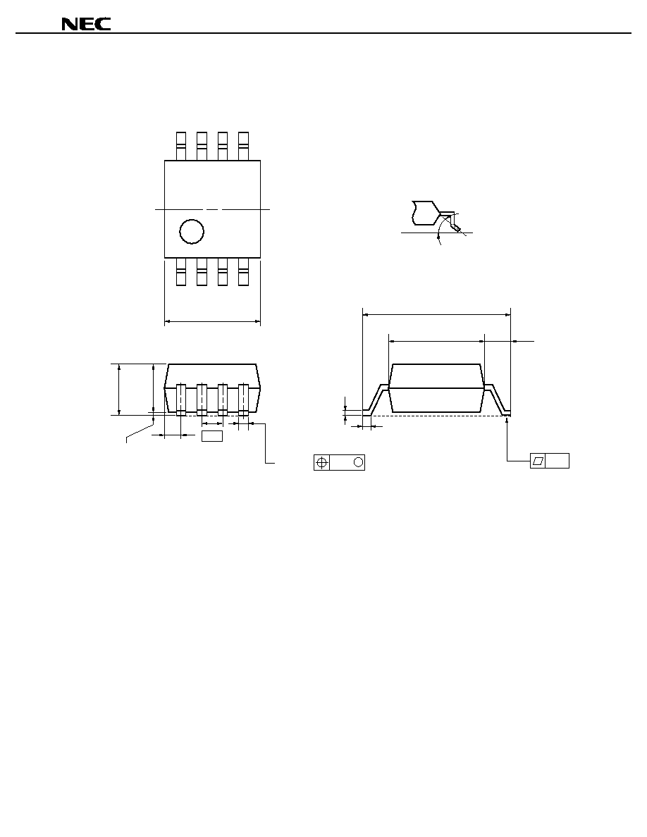
PACKAGE DIMENSIONS
8 PIN PLASTIC SHRINK SOP (175 mil) (Unit: mm)
8
5
1
4
3.0 MAX.
1.5 ± 0.1
1.8 MAX.
0.1 ± 0.1
0.575 MAX.
0.65
0.3
+0.10
≠0.05
0.10
M
0.15
0.15
+0.10
≠0.05
0.5 ± 0.2
3.2 ± 0.1
4.94 ± 0.2
0.87 ± 0.2
Detail of lead end
3∞
+7∞
≠3∞
6
µ
µ
µ
µ
PG139GV
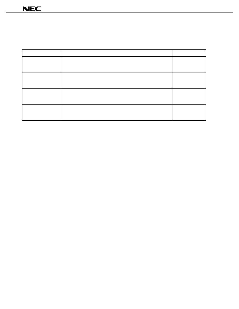
RECOMMENDED SOLDERING CONDITIONS
This product should be soldered in the following recommended conditions. Other soldering methods and
conditions than the recommended conditions are to be consulted with our sales representatives.
Soldering process
Soldering Conditions
Symbol
Infrared Ray Reflow
Peak package's surface temperature: 235∞C or below
Reflow time: 30 seconds or less (at 210∞C)
Number of reflow process: 3, Exposure limit
Note
: None
IR35-00-3
VPS
Peak package's surface temperature: 215∞C or below
Reflow time: 40 seconds or less (at 200∞C)
Number of reflow process: 3, Exposure limit
Note
: None
VP15-00-3
Wave Soldering
Solder temperature: 260∞C or below
Flow time: 10 seconds or less
Number of flow process: 1, Exposure limit
Note
: None
WS60-00-1
Partial Heating Method
Terminal temperature: 300∞C
Flow time: 3 seconds or less (per one pin),
Exposure limit
Note
: None
Note
Exposure limit before soldering after dry-pack package is opened.
Storage conditions: 25∞C and relative humidity at 65% or less.
Caution
Do not apply more than a single process at once, except for "partial heating method".

7
µ
µ
µ
µ
PG139GV
[MEMO]

µ
µ
µ
µ
PG139GV
Caution
The Great Care must be taken in dealing with the devices in this guide.
The reason is that the material of the devices is GaAs (Gallium Arsenide), which is
designated as harmful substance according to the law concerned.
Keep the law concerned and so on, especially in case of removal.
The application circuits and their parameters are for reference only and are not intended for use in actual design-ins.
No part of this document may be copied or reproduced in any form or by any means without the prior written
consent of NEC Corporation. NEC Corporation assumes no responsibility for any errors which may appear in this
document.
NEC Corporation does not assume any liability for infringement of patents, copyrights or other intellectual
property rights of third parties by or arising from use of a device described herein or any other liability arising
from use of such device. No license, either express, implied or otherwise, is granted under any patents,
copyrights or other intellectual property rights of NEC Corporation or others.
While NEC Corporation has been making continuous effort to enhance the reliability of its semiconductor devices,
the possibility of defects cannot be eliminated entirely. To minimize risks of damage or injury to persons or
property arising from a defect in an NEC semiconductor device, customers must incorporate sufficient safety
measures in its design, such as redundancy, fire-containment, and anti-failure features.
NEC devices are classified into the following three quality grades:
"Standard", "Special", and "Specific". The Specific quality grade applies only to devices developed based on
a customer designated "quality assurance program" for a specific application. The recommended applications
of a device depend on its quality grade, as indicated below. Customers must check the quality grade of each
device before using it in a particular application.
Standard: Computers, office equipment, communications equipment, test and measurement equipment,
audio and visual equipment, home electronic appliances, machine tools, personal electronic
equipment and industrial robots
Special: Transportation equipment (automobiles, trains, ships, etc.), traffic control systems, anti-disaster
systems, anti-crime systems, safety equipment and medical equipment (not specifically designed
for life support)
Specific: Aircrafts, aerospace equipment, submersible repeaters, nuclear reactor control systems, life
support systems or medical equipment for life support, etc.
The quality grade of NEC devices is "Standard" unless otherwise specified in NEC's Data Sheets or Data Books.
If customers intend to use NEC devices for applications other than those specified for Standard quality grade,
they should contact an NEC sales representative in advance.
Anti-radioactive design is not implemented in this product.
M4 96. 5