The information in this document is subject to change without notice. Before using this document, please
confirm that this is the latest version.
Not all devices/types available in every country. Please check with local NEC representative for
availability and additional information.
GaAs INTEGRATED CIRCUIT
µ
µ
µ
µ
PG153TB
L-BAND SPDT SWITCH
Document No. P13632EJ2V0DS00 (2nd edition)
Date Published September 1999 N CP(K)
Printed in Japan
DATA SHEET
1998, 1999
©
The mark
shows major revised points.
DESCRIPTION
The
µ
PG153TB is an L-band SPDT (Single Pole Double Throw) GaAs FET switch which was developed for digital
cellular or cordless telephone application. The device can operate from 100 MHz to 2.5 GHz, having the low
insertion loss. It housed in an original 6-pin super minimold package that is smaller than usual 6-pin minimold easy
to install and contributes to miniaturizing the system.
FEATURES
∑
Low Insertion Loss
: L
INS
= 0.7 dB TYP. @V
CONT
= +3.0 V/0 V, f = 2 GHz
∑
High Linearity Switching: P
in (1 dB)
= +33.0 dBm TYP. @V
CONT
= +3.0 V/0 V, f = 2 GHz
∑
Small 6-pin super minimold package (Size: 2.0
◊
1.25
◊
0.9 mm)
APPLICATIONS
∑
L, S-band digital cellular or cordless telephone
∑
PCS, WLAN, and WLL applications
ORDERING INFORMATION
Part Number
Marking
Package
Supplying Form
µ
PG153TB-E3
G1J
6-pin super minimold
Embossed tape 8 mm wide.
Pin 1, 2, 3 face to tape perforation side.
Qty 3 kp/reel.
Remark To order evaluation samples, please contact your local NEC sales office. (Part number for sample
order:
µ
PG153TB)
ABSOLUTE MAXIMUM RATINGS (T
A
= +25∞C)
Parameter
Symbol
Ratings
Unit
Control Voltage 1, 2
V
CONT1, 2
≠6.0 to +6.0
Note
V
Input Power
P
in
+33
dBm
Total Power Dissipation
P
tot
0.15
W
Operating Temperature
T
A
≠45 to +85
∞C
Storage Temperature
T
stg
≠55 to +150
∞C
Note
Condition 2.5
| V
CONT1
≠ V
CONT2
|
6.0 V
Remarks 1. Mounted on a 50
◊
50
◊
1.6 mm double copper clad epoxy glass PWB, T
A
= +85∞C
2. Operation in excess of any one of these parameters may result in permanent damage.
Caution
The IC must be handled with care to prevent static discharge because its circuit is composed of
GaAs MES FET.

Data Sheet P13632EJ2V0DS00
2
µ
µ
µ
µ
PG153TB
PIN CONNECTIONS
Pin No.
Connection
Pin No.
Connection
1
OUT1
4
V
CONT2
2
GND
5
IN
3
OUT2
6
V
CONT1
RECOMMENDED OPERATING CONDITIONS (T
A
= +25∞C)
Parameter
Symbol
MIN.
TYP.
MAX.
Unit
Control Voltage (Low)
V
CONT
≠0.2
0
+0.2
V
Control Voltage (High)
V
CONT
+2.5
+3.0
+5.3
V
ELECTRICAL CHARACTERISTICS
(Unless otherwise specified, T
A
= +25∞C, V
CONT1
= 3 V, V
CONT2
= 0 V or V
CONT1
= 0 V, V
CONT2
= 3 V, Z
O
= 50
,
Off chip DC blocking capacitors value; 51 pF)
Parameter
Symbol
Test Conditions
MIN.
TYP.
MAX.
Unit
f = 100 M to 1.0 GHz
-
0.50
0.65
f = 2.0 GHz
-
0.70
0.90
Insertion Loss
L
INS
f = 2.5 GHz
-
0.90
Note 1
-
dB
f = 100 M to 2.0 GHz
10
13
-
f = 1.0 GHz
15
18.5
-
Isolation
ISL
f = 2.5 GHz
-
10
Note 1
-
dB
Input Return Loss
RL
in
f = 100 M to 2.0 GHz
11
15
-
dB
Output Return Loss
RL
out
f = 100 M to 2.0 GHz
11
15
-
dB
Input Power at 0.1 dB
Compression Point
Note 2
P
in (0.1 dB)
f = 2.0 GHz
-
29
-
dBm
Input Power at 1 dB
Compression Point
Note 2
P
in (1 dB)
f = 2.0 GHz
31
33
-
dBm
Switching Speed
t
sw
-
30
-
ns
Control Current
I
CONT
V
CONT
= 3 V/0 V
-
20
50
µ
A
Notes 1. Characteristic for reference at f = 2.0 to 2.5 GHz
2. P
in (0.1 dB)
or P
in (1 dB)
is measured the input power level when the insertion loss increases more 0.1 dB or
1 dB than that of linear range. All other characteristics are measured in linear range.
Cautions 1. When the
µ
µ
µ
µ
PG153TB is used, it is necessary to use DC blocking capacitors for No. 1 (OUT1),
No. 3 (OUT2) and No. 5 (IN). The value of DC blocking capacitors should be chosen to
accommodate the frequency of operation, band width, switching speed and the condition
with actual board of your system.
The range of recommended DC blocking capacitor value is less than 100 pF.
2. The distance between IC's GND pin and ground pattern of substrate should be as shorter as
possible to avoid parasitic parameters.
3
4
2
5
1
6
4
3
5
2
6
1
G1J
(Top View)
(Bottom View)
Data Sheet P13632EJ2V0DS00
3
µ
µ
µ
µ
PG153TB
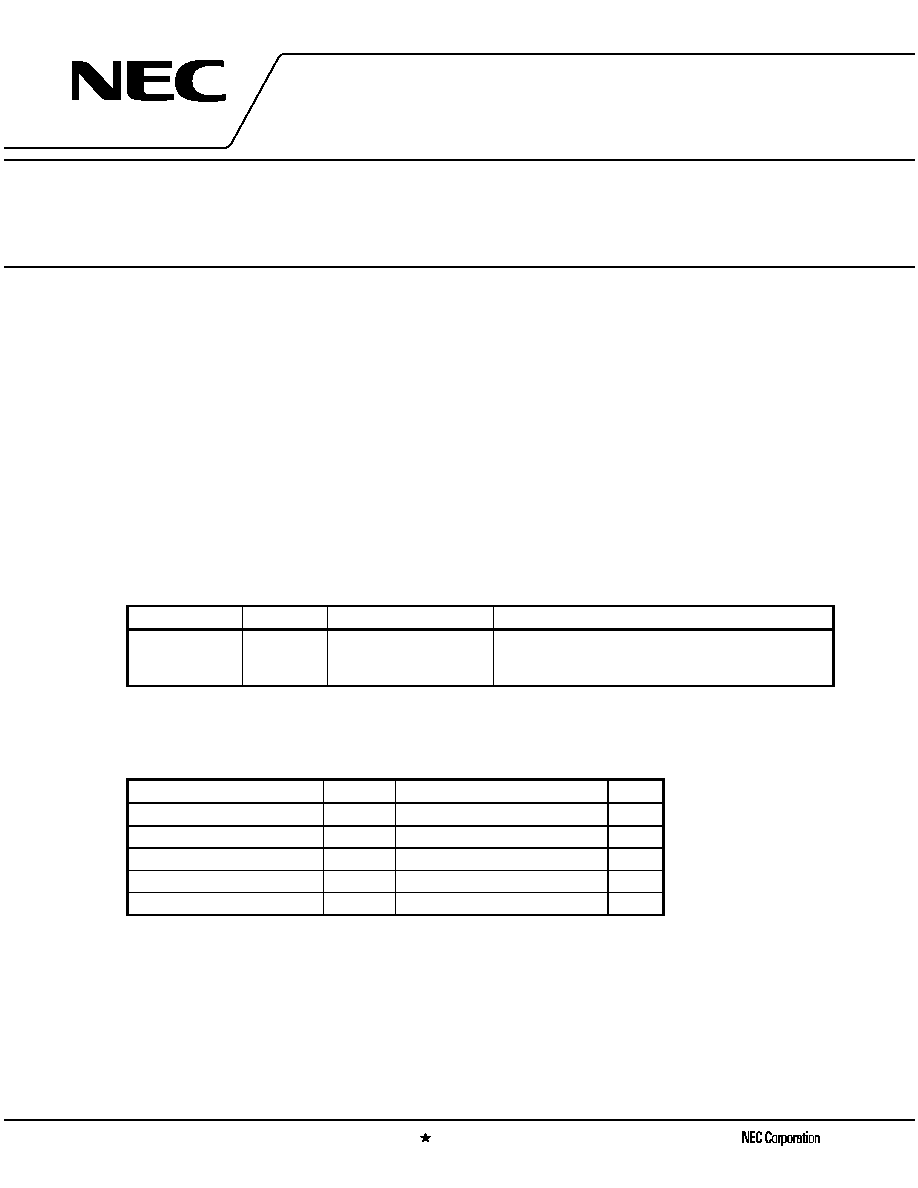
TYPICAL CHARACTERISTICS (ON)
TEST CONDITIONS: V
CONT
= 3 V/0 V, P
in
= 0 dBm, T
A
= +25
∞
C
0
≠10
Input Return Loss RL
in
(dB)
≠20
≠30
≠40
START 0.300 000 000 GHz
CH1 S
11
10 dB/REF 0 dB
Frequency f (GHz)
IN-OUT1 INPUT RETURN LOSS vs. FREQUENCY
STOP 3.300 000 000 GHz
Isolation ISL (dB)
START 0.300 000 000 GHz
CH1 S
12
log MAG
log MAG
10 dB/REF 0 dB
Frequency f (GHz)
IN-OUT1 ISOLATION vs. FREQUENCY
STOP 3.300 000 000 GHz
3
2
4
1
3
2
4
Output Return Loss RL
out
(dB)
START 0.300 000 000 GHz
CH1 S
22
log MAG
10 dB/REF 0 dB
Frequency f (GHz)
IN-OUT1 OUTPUT RETURN LOSS vs. FREQUENCY
STOP 3.300 000 000 GHz
4
Insertion Loss L
INS
(dB)
START 0.300 000 000 GHz
CH1 S
21
log MAG
1 dB/REF 0 dB
Frequency f (GHz)
IN-OUT1 INSERTION LOSS vs. FREQUENCY
STOP 3.300 000 000 GHz
4
1
3
2
4
1
3
2
4
1
1: ≠24.057 dB
1 GHz
2: ≠37.231 dB
1.5 GHz
3: ≠25.963 dB
2 GHz
4: ≠19.332 dB
2.5 GHz
1: ≠0.764 dB
1 GHz
2: ≠0.957 dB
1.5 GHz
3: ≠1.215 dB
2 GHz
4: ≠1.516 dB
2.5 GHz
MARKER 1
1 GHz
MARKER 1
1 GHz
MARKER 1
1 GHz
0
≠10
≠20
≠30
≠40
MARKER 1
1 GHz
0
≠10
≠20
≠30
≠40
0
≠1
≠2
≠3
≠4
1: ≠18.937 dB
1 GHz
2: ≠15.032 dB
1.5 GHz
3: ≠12.119 dB
2 GHz
4: ≠10.675 dB
2.5 GHz
1: ≠22.622 dB
1 GHz
2: ≠28.228 dB
1.5 GHz
3: ≠27.318 dB
2 GHz
4: ≠18.235 dB
2.5 GHz
IN
OUT1
OUT2
50
Caution This data is including loss of the test fixture.
Data Sheet P13632EJ2V0DS00
4
µ
µ
µ
µ
PG153TB
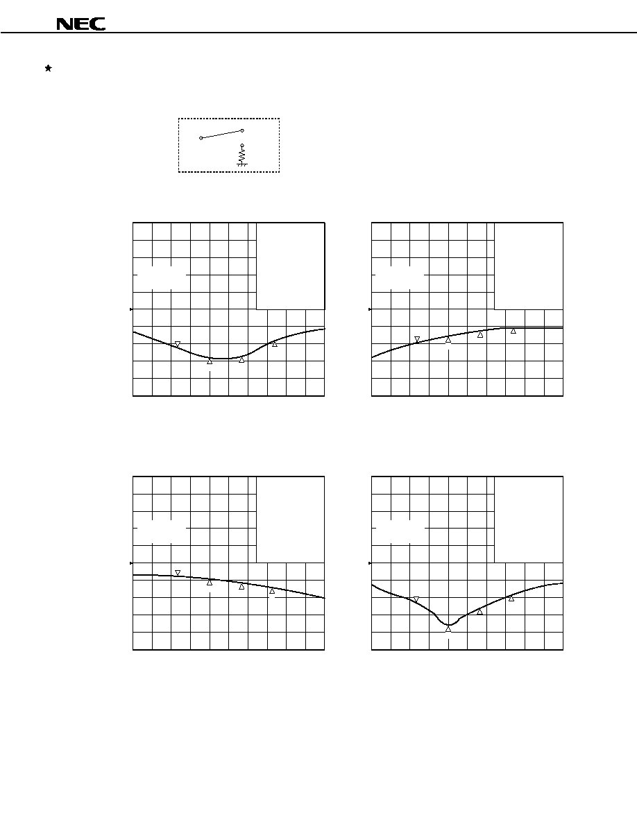
TYPICAL CHARACTERISTICS (OFF)
TEST CONDITIONS: V
CONT
= 3 V/3 V, P
in
= 0 dBm, T
A
= +25
∞
C
0
≠10
Input Return Loss RL
in
(dB)
≠20
≠30
≠40
START 0.300 000 000 GHz
CH1 S
11
log MAG
10 dB/REF 0 dB
Frequency f (GHz)
IN-OUT1 INPUT RETURN LOSS vs. FREQUENCY
STOP 3.300 000 000 GHz
1: ≠10.653 dB
1 GHz
2: ≠11.354 dB
1.5 GHz
3: ≠11.745 dB
2 GHz
4: ≠11.111 dB
2.5 GHz
0
≠10
Output Return Loss RL
out
(dB)
≠20
≠30
≠40
START 0.300 000 000 GHz
CH1 S
22
log MAG
10 dB/REF 0 dB
Frequency f (GHz)
IN-OUT1 OUTPUT RETURN LOSS vs. FREQUENCY
STOP 3.300 000 000 GHz
0
≠10
Insertion Loss L
INS
(dB)
≠20
≠30
≠40
START 0.300 000 000 GHz
CH1 S
21
log MAG
10 dB/REF 0 dB
Frequency f (GHz)
IN-OUT1 INSERTION LOSS vs. FREQUENCY
STOP 3.300 000 000 GHz
3
2
4
1
2
4
1
3
2
4
1
1: ≠12.642 dB
1 GHz
2: ≠12.038 dB
1.5 GHz
3: ≠11.728 dB
2 GHz
4: ≠12.291 dB
2.5 GHz
1: ≠4.066 dB
1 GHz
2: ≠4.072 dB
1.5 GHz
3: ≠4.130 dB
2 GHz
4: ≠4.382 dB
2.5 GHz
MARKER 1
1 GHz
MARKER 1
1 GHz
MARKER 1
1 GHz
3
IN
OUT1
OUT2
50
Caution This data is including loss of the test fixture.

Data Sheet P13632EJ2V0DS00
5
µ
µ
µ
µ
PG153TB
TEST CIRCUIT
T
A
= +25∞C, V
CONT1
= +3 V, V
CONT2
= 0 V or V
CONT1
= 0 V, V
CONT2
= +3 V, f = 2 GHz, Z
O
= 50
Off chip DC blocking capacitors value: C0 = 51 pF, C1 = 1 000 pF (Bypass), using NEC standard evaluation board
4
5
6
3
2
1
G1J
C1
C0
C1
V
CONT2
IN
V
CONT1
C0
C0
OUT1
OUT2
EVALUATION BOARD
OUT1
V
CONT1
OUT2
V
CONT2
IN
Data Sheet P13632EJ2V0DS00
6
µ
µ
µ
µ
PG153TB
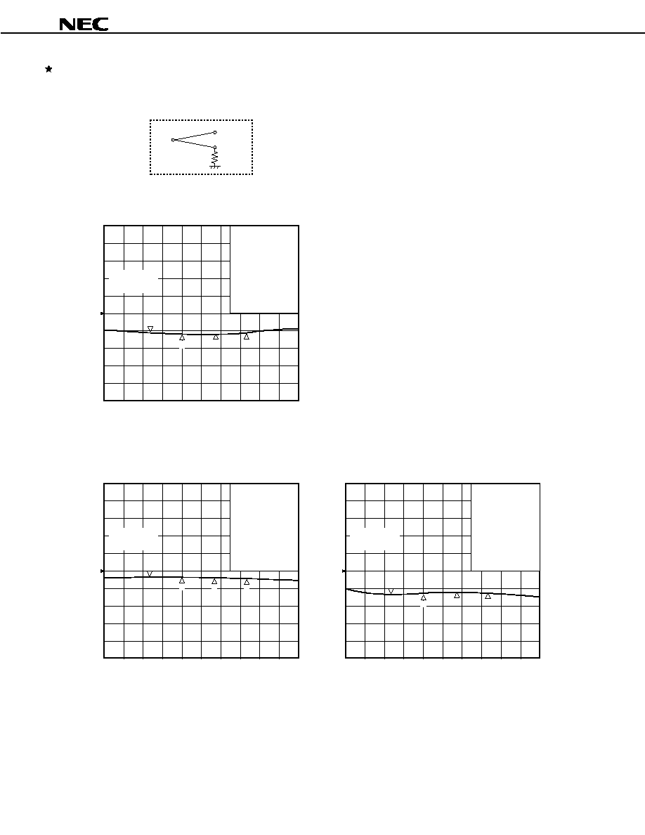
TRUTH TABLE OF SWITCHING BY CONDITION OF CONTROL VOLTAGE
V
CONT1
V
CONT1(H)
V
CONT(L)
V
CONT(H)
IN
OUT1
OUT2
Note
IN
OUT1
OUT2
V
CONT2
V
CONT(L)
IN
OUT1
OUT2
IN
OUT1
OUT2
Note
Note In case of V
CONT1
= V
CONT2
= High or V
CONT1
= V
CONT2
= Low, (that is same control voltage for both pins),
input signal of IN (Pin 5) is output from OUT1 (Pin 1) and OUT2 (Pin 3).
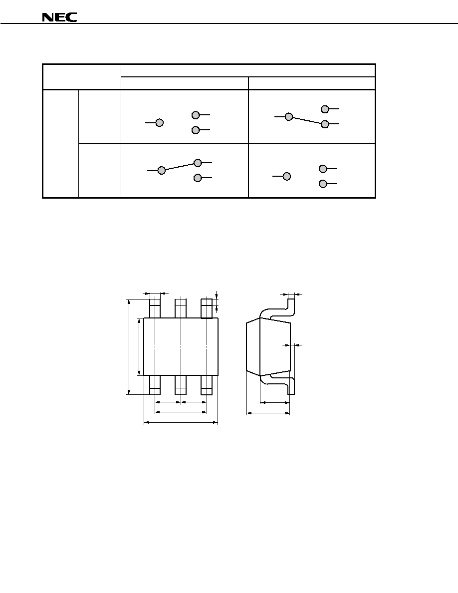
PACKAGE DIMENSIONS
6 PIN MINIMOLD (Unit: mm)
0 to 0.1
0.15
0.7
0.9
±
0.1
0.65
0.65
1.3
2.0
±
0.2
0.1 MIN.
0.2
+0.1
≠0
+0.1
≠0
2.1
±
0.1
1.25
±
0.1
Data Sheet P13632EJ2V0DS00
7
µ
µ
µ
µ
PG153TB
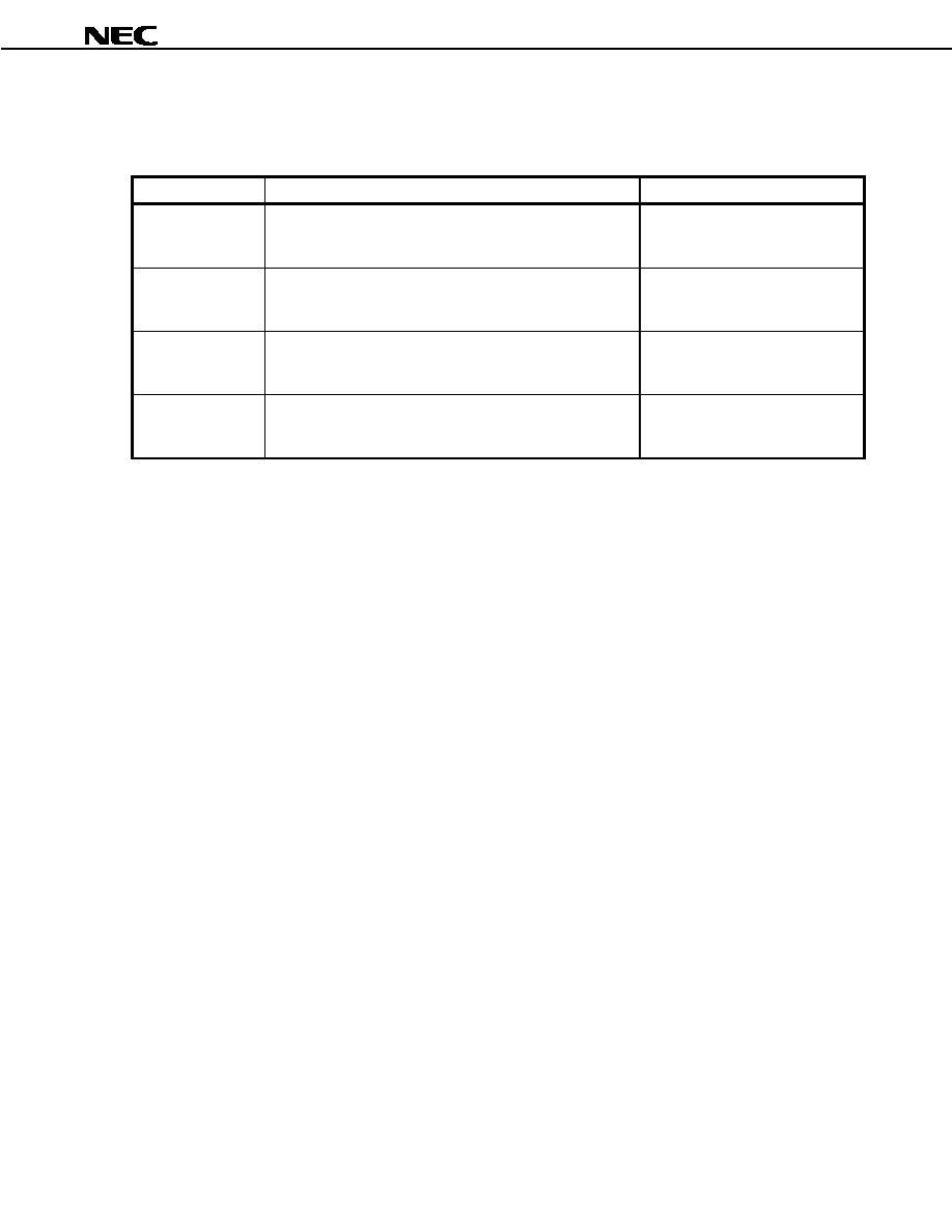
RECOMMENDED SOLDERING CONDITIONS
This product should be soldered under the following recommended conditions. For soldering method and
conditions other than those recommended below, contact your NEC sales representative.
Soldering Method
Soldering Conditions
Recommended Condition Symbol
Infrared Reflow
Package peak temperature: 235∞C or below
Time: 30 seconds or less (at 210∞C)
Count: 3, Exposure limit: None
Note
IR35-00-3
VPS
Package peak temperature: 215∞C or below
Time: 40 seconds or less (at 200∞C)
Count: 3, Exposure limit: None
Note
VP15-00-3
Wave Soldering
Soldering bath temperature: 260∞C or below
Time: 10 seconds or less
Count: 1, Exposure limit: None
Note
WS60-00-1
Partial Heating
Pin temperature: 300∞C
Time: 3 seconds or less (per pin row)
Exposure limit: None
Note
≠
Note After opening the dry pack, keep it in a place below 25∞C and 65% RH for the allowable storage period.
Caution Do not use different soldering methods together (except for partial heating).
µ
µ
µ
µ
PG153TB
Caution
The Great Care must be taken in dealing with the devices in this guide.
The reason is that the material of the devices is GaAs (Gallium Arsenide), which is
designated as harmful substance according to the law concerned.
Keep the law concerned and so on, especially in case of removal.
∑
The information in this document is subject to change without notice. Before using this document, please
confirm that this is the latest version.
∑
No part of this document may be copied or reproduced in any form or by any means without the prior written
consent of NEC Corporation. NEC Corporation assumes no responsibility for any errors which may appear in
this document.
∑
NEC Corporation does not assume any liability for infringement of patents, copyrights or other intellectual property
rights of third parties by or arising from use of a device described herein or any other liability arising from use
of such device. No license, either express, implied or otherwise, is granted under any patents, copyrights or other
intellectual property rights of NEC Corporation or others.
∑
Descriptions of circuits, software, and other related information in this document are provided for illustrative
purposes in semiconductor product operation and application examples. The incorporation of these circuits,
software, and information in the design of the customer's equipment shall be done under the full responsibility
of the customer. NEC Corporation assumes no responsibility for any losses incurred by the customer or third
parties arising from the use of these circuits, software, and information.
∑
While NEC Corporation has been making continuous effort to enhance the reliability of its semiconductor devices,
the possibility of defects cannot be eliminated entirely. To minimize risks of damage or injury to persons or
property arising from a defect in an NEC semiconductor device, customers must incorporate sufficient safety
measures in its design, such as redundancy, fire-containment, and anti-failure features.
∑
NEC devices are classified into the following three quality grades:
"Standard", "Special", and "Specific". The Specific quality grade applies only to devices developed based on a
customer designated "quality assurance program" for a specific application. The recommended applications of
a device depend on its quality grade, as indicated below. Customers must check the quality grade of each device
before using it in a particular application.
Standard: Computers, office equipment, communications equipment, test and measurement equipment,
audio and visual equipment, home electronic appliances, machine tools, personal electronic
equipment and industrial robots
Special: Transportation equipment (automobiles, trains, ships, etc.), traffic control systems, anti-disaster
systems, anti-crime systems, safety equipment and medical equipment (not specifically designed
for life support)
Specific: Aircraft, aerospace equipment, submersible repeaters, nuclear reactor control systems, life
support systems or medical equipment for life support, etc.
The quality grade of NEC devices is "Standard" unless otherwise specified in NEC's Data Sheets or Data Books.
If customers intend to use NEC devices for applications other than those specified for Standard quality grade,
they should contact an NEC sales representative in advance.
M7 98. 8