The information in this document is subject to change without notice.
GaAs INTEGRATED CIRCUIT
µ
µ
µ
µ
PG175TA
L-Band PA DRIVER AMPLIFIER
1998
©
PRELIMINARY DATA SHEET
Document No. P13470EJ1V0DS00 (1st edition)
Date Published May 1998 N CP(K)
Printed in Japan
DESCRIPTION
µ
PG175TA is a GaAs MMIC for PA driver amplifier with variable gain function which was developed for PDC
(Personal Digital Cellular in Japan) and another L-band application. The device can operate with 3.0 V, having the
high gain and low distortion.
FEATURES
∑
Low Operation Voltage: V
DD1
= V
DD2
= 3.0 V
∑
f
RF
: 925 to 960 MHz@ P
out
= +9 dBm
∑
Low distortion: P
adj1
= ≠60 dBc typ. @ V
DD
= 3.0 V, P
out
= +9 dBm, V
AGC
= 2.5 V
External input and output matching
∑
Low operation Current: I
DD
= 20 mA typ. @ V
DD
= 3.0 V, P
out
= +9 dBm, V
AGC
= 2.5 V
External input and output matching
∑
Variable gain control function:
G = 35 dB typ. @ V
AGC
= 0.5 to 2.5 V
∑
6 pin mini-mold package
APPLICATION
∑
Digital Cellular: PDC800M, etc.
ORDERING INFORMATION (PLAN)
PART NUMBER
PACKAGE
PACKING FORM
µ
PG175TA-E3
6 pin Mini-mold
Carrier tape width is 8 mm, Quantity is 3 kpcs per reel.
Remark For sample order, please contact your local NEC sales office. (Part number for sample order:
µ
PG175TA)
Caution The IC must be handled with care to prevent static discharge because its circuit composed of
GaAs HJ-FET.
Preliminary Data Sheet
2
µ
µ
µ
µ
PG175TA
ABSOLUTE MAXIMUM RATINGS (T
A
= 25∞C)
PARAMETERS
SYMBOL
RATINGS
UNIT
Supply Voltage
V
DD1
, V
DD2
6.0
V
AGC Control Voltage
V
AGC
6.0
V
Input Power
P
in
≠8
dBm
Total Power Dissipation
P
tot
200
Note
mW
Operating Temperature
T
A
≠30 to +90
∞C
Storage Temperature
T
stg
≠35 to +150
∞C
Note Mounted on a 50
◊
50
◊
1.6 mm double copper clad epoxy glass PWB, T
A
= +85∞C
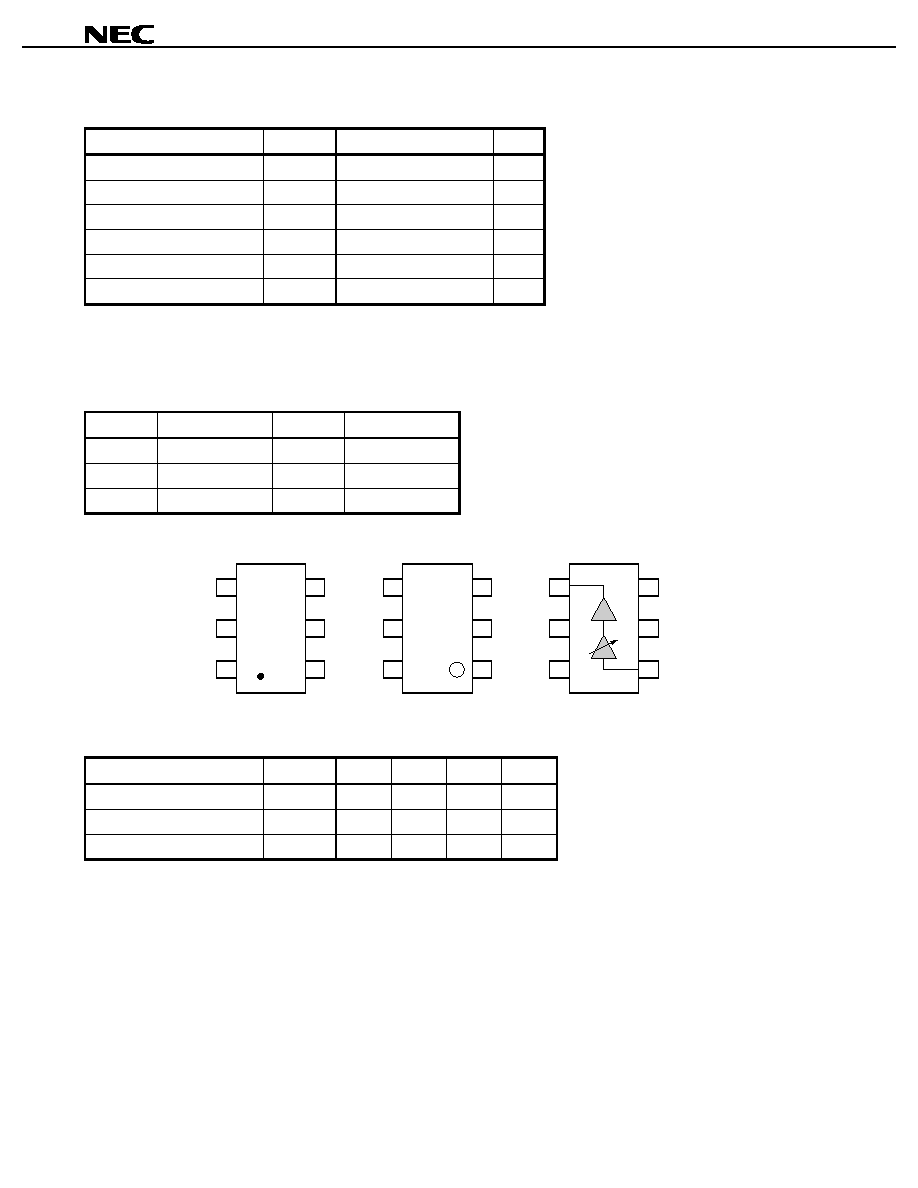
PIN CONNECTION AND INTERNAL BLOCK DIAGRAM
PIN NO.
CONNECTION
PIN NO.
CONNECTION
1
V
DD1
4
V
AGC
2
GND
5
GND
3
V
DD2
& OUT
6
IN
3
Top View
2
G1E
1
4
5
6
3
Bottom View
2
1
4
5
6
3
Top View
2
1
4
5
6
RECOMMENDED OPERATING CONDITIONS (T
A
= 25∞C)
PARAMETERS
SYMBOL
MIN.
TYP.
MAX.
UNIT
Supply Voltage
V
DD1
, V
DD2
+2.7
+3.0
+3.3
V
AGC Control Voltage
V
AGC
0.5
2.5
V
Input Power
P
in
≠21
≠17
dBm
Preliminary Data Sheet
3
µ
µ
µ
µ
PG175TA
ELECTRICAL CHARACTERISTICS
(Unless otherwise specified, T
A
= 25∞C, V
DD1
= V
DD2
= +3.0 V,
/4DQPSK modulated signal input,
External input and output matching)
PARAMETERS
SYMBOL
TEST CONDITIONS
MIN.
TYP.
MAX.
UNIT
Operating Frequency
f
925
960
MHz
Total Current
I
DD
P
in
= ≠21 dBm, V
AGC
= 2.5 V
20
30
mA
AGC Control Current
I
AGC
V
AGC
= 0.5 to 2.5 V
200
500
µ
A
Power Gain
G
p
P
in
= ≠21 dBm, V
AGC
= 2.5 V
27
30
dB
Variable Gain Range
G
P
in
= ≠21 dBm, V
AGC
= 0.5 to 2.5 V
30
35
dB
Adjacent Channel Power
Leakage 1
P
adj1
P
out
= +9 dBm, V
AGC
= 2.5 V
f =
±
50 kHz, 21 kHz Band Width
≠60
≠55
dBc
Adjacent Channel Power
Leakage 2
P
adj2
P
out
= +9 dBm, V
AGC
= 2.5 V
f =
±
100 kHz, 21 kHz Band Width
≠70
≠65
dBc
Input Return Loss
RL
in
External matching
10
dB
Output Return Loss
RL
out
External matching
10
dB

Preliminary Data Sheet
5
µ
µ
µ
µ
PG175TA
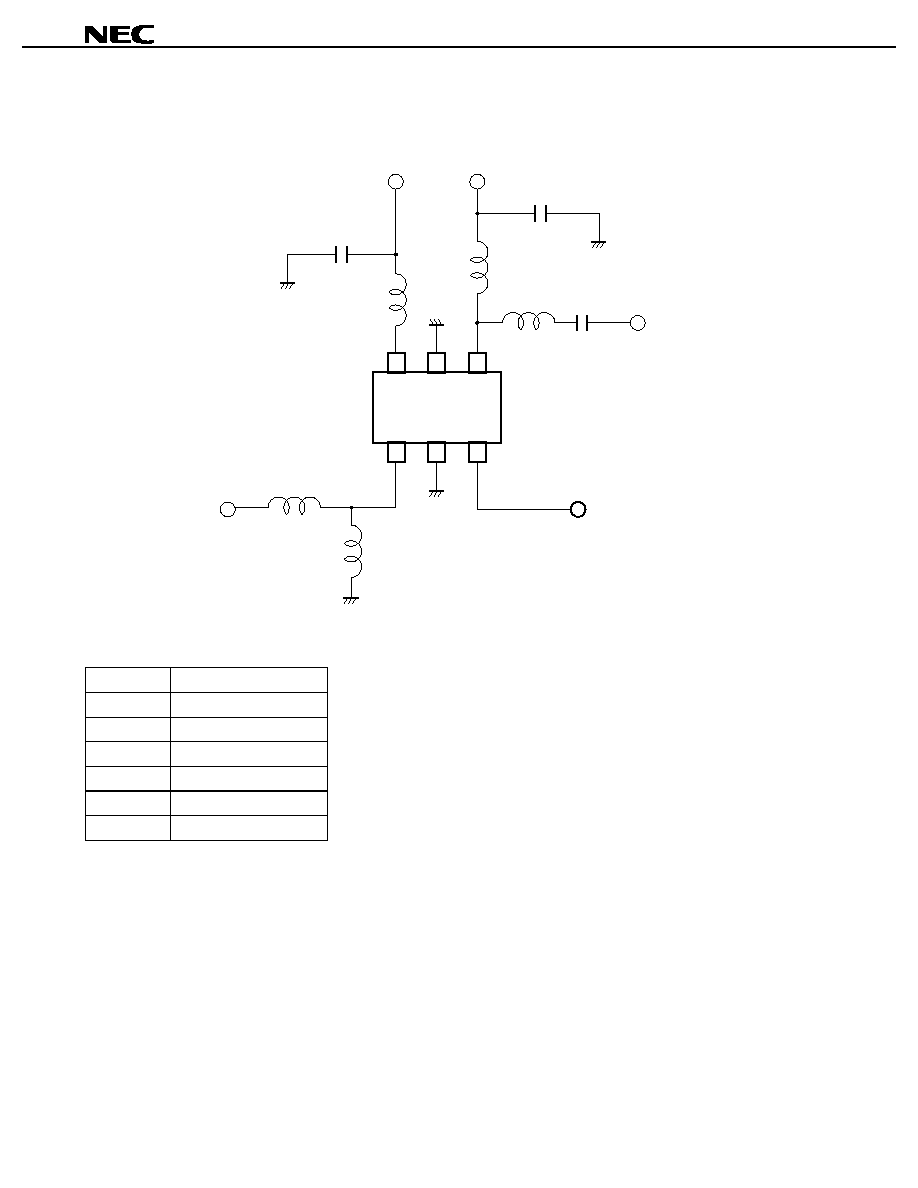
EVALUATION BOARD (Epoxy Glass,
= 4.6, 0.4 mm thickness)
OUT
C1
C2
L3
C3
L5
L2
L1
V
DD2
V
AGC
IN
V
DD1
L4
40 mm
38 mm
6 PIN MINI-MOLD PACKAGE DIMENSIONS (UNIT: mm)
2.8
+0.2
≠0.3
0 to 0.1
1.5
+0.2
≠0.1
0.3
+0.1
≠0.0
1
2
3
6
5
4
0.95
0.95
1.9
2.9
±
0.2
0.13
±
0.1
0.8
1.1
+0.2
≠0.1