 | –≠–ª–µ–∫—Ç—Ä–æ–Ω–Ω—ã–π –∫–æ–º–ø–æ–Ω–µ–Ω—Ç: UPG181GR | –°–∫–∞—á–∞—Ç—å:  PDF PDF  ZIP ZIP |

The information in this document is subject to change without notice. Before using this document, please
confirm that this is the latest version.
Not all devices/types available in every country. Please check with local NEC representative for
availability and additional information.
GaAs INTEGRATED CIRCUIT
µ
µ
µ
µ
PG181GR
GaAs MMIC DBS Twin IF Switch
Document No. P14268EJ2V0DS00 (2nd edition)
Date Published November 1999 N CP(K)
Printed in Japan
DATA SHEET
1999
©
The mark
shows major revised points.
DESCRIPTION
The
µ
PG181GR is intended for use in Direct Broadcast Satellite (DBS) applications within the Low Noise Block
(LNB) down-converter for systems where at least two LNB outputs are required.
It offers two intermediate frequency amplifier channels that can independently select 1 of 2 IF inputs. It is loused
in a very small 16-pin plastic HTSSOP package available on tape-and-reel and easy to install and contributes to
miniaturizing the systems.
FEATURES
∑ Two Independent IF Channels
∑ Integral Switching to Channel Input to Either Channel Output
∑ Insertion Loss Per Channel
: 5.0 dB TYP. (Z
O
= 50
)
∑ Frequency Range
: 950 MHz to 2 150 MHz
∑ Channel to Channel Isolation
: 33 dB TYP.
∑ Small 16-pin HTSSOP Package
ORDERING INFORMATION (PLAN)
Part Number
Package
Supplying Form
µ
PG181GR-E1
16-pin Plastic HTSSOP
Carrier tape width 12 mm.
Qty 3 kp/reel.
Remark To order evaluation samples, please contact your local NEC sales office. (Part number for sample
order:
µ
PG181GR)
Caution The IC must be handled with care to prevent static discharge because its circuit composed of
GaAs MES-FET.

Data Sheet P14268EJ2V0DS00
2
µ
µ
µ
µ
PG181GR
ABSOLUTE MAXIMUM RATINGS (T
A
= +25
∞
∞
∞
∞
C)
Parameter
Symbol
Ratings
Unit
Control Voltage 1, 2, 3, 4
V
CONT1, 2, 3, 4
-
6 to +6
Note 1
V
Total Power Dissipation
P
tot
2
Note2
W
Operating Ambient Temperature
T
A
-
40 to +85
∞
C
Storage Temperature
T
stg
-
65 to +150
∞
C
Notes 1. | V
CONT(H)
-
V
CONT(L)
|
6.0 V
2. Mounted on 50
◊
50
◊
1.6 mm double copper clad epoxy glass PWB, T
C
= +85
∞
C
PIN CONNECTION AND INTERNAL BLOCK DIAGRAM (TOP VIEW)
Pin No.
Connection
Pin No.
Connection
Pin No.
Connection
Pin No.
Connection
1
IN2
5
V
CONT4
9
OUT1
13
V
CONT1
2
GND
6
GND
10
GND
14
GND
3
GND
7
GND
11
GND
15
GND
4
V
CONT3
8
OUT2
12
V
CONT2
16
IN1
16
15
14
13
12
11
10
9
1
2
3
4
5
6
7
8
Data Sheet P14268EJ2V0DS00
3
µ
µ
µ
µ
PG181GR
RECOMMENDED OPERATING CONDITIONS (T
A
= +25
∞
∞
∞
∞
C)
Parameter
Symbol
MIN.
TYP.
MAX.
Unit
Control Voltage (High)
V
CONT(H)
+4.5
+5
+5.5
V
Control Voltage (Low)
V
CONT(L)
-
0.5
0
+0.5
V
ELECTRICAL CHARACTERISTICS (T
A
= +25
∞
∞
∞
∞
C, unless otherwise specified: V
CONT1
to V
CONT4
=
0/ +5 V, Z
O
= 50
, LL, LR, RL, RR Each Port)
Parameter
Symbol
Test Conditions
MIN.
TYP.
MAX.
Unit
Insertion Loss
L
INS
f = 0.95 GHz to 2.15 GHz
-
5.0
7.0
dB
Insertion Loss Flatness
L
INS
| L
INS
(0.95 GHz)
-
L
INS
(1.7 GHz) |
-
0.5
1.2
dB
Insertion Loss Flatness
L
INS
| L
INS
(0.95 GHz)
-
L
INS
(2.15 GHz) |
-
0.8
1.5
dB
Channel Isolation
ISL
f = 0.95 GHz to 1.7 GHz
30
33
-
dB
Channel Isolation
ISL
f = 1.7 GHz to 2.15 GHz
25
30
-
dB
Output Return Loss
RL
out
f = 0.95 GHz to 2.15 GHz
13
16
-
dB
Control Current
I
CONT
V
CONT
= +5 V/0 V, RF OFF
-
-
200
µ
A

Data Sheet P14268EJ2V0DS00
4
µ
µ
µ
µ
PG181GR
EVALUATION CIRCUIT
V
CONT1
to V
CONT4
= 0/ +5 V, Z
O
= 50
, DC Blocking Capacitor = 51 pF
16
1
9
8
V
CONT1
V
CONT2
V
CONT3
V
CONT4
C = 51 pF
C = 51 pF
C = 51 pF
C = 51 pF
Z
O
= 50
Z
O
= 50
Z
O
= 50
Z
O
= 50
IN1
(L)
IN2
(R)
OUT1
OUT2
1 000 pF
1 000 pF
1 000 pF
1 000 pF
CHANNEL SELECT TRUTH TABLE
Output
Control Pin
OUT1
OUT2
On Channel
V
CONT1
V
CONT2
V
CONT3
V
CONT4
L
L
IN1
-
OUT1
IN1
-
OUT2
Low
High
High
Low
L
R
IN1
-
OUT1
IN2
-
OUT2
Low
High
Low
High
R
L
IN2
-
OUT1
IN1
-
OUT2
High
Low
High
Low
R
R
IN2
-
OUT1
IN2
-
OUT2
High
Low
Low
High

Data Sheet P14268EJ2V0DS00
5
µ
µ
µ
µ
PG181GR
TYPICAL CHARACTERISTICS (T
A
= +25
∞
∞
∞
∞
C)
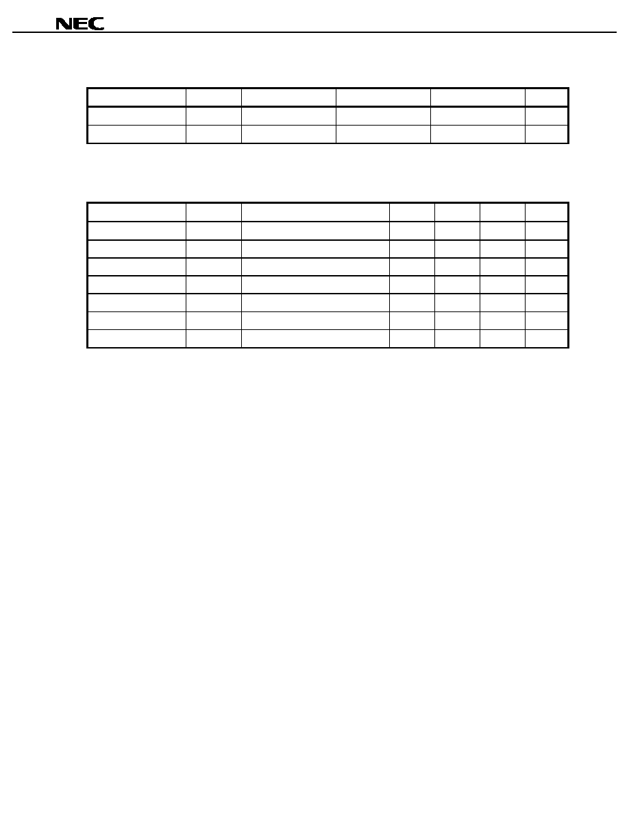
1
2
3
1:
2:
3:
≠4.49 dB
0.95 GHz
≠4.93 dB
1.7 GHz
≠5.31 dB
2.15 GHz
0
≠10
≠20
START 0.050 000 000 GHz
STOP 5.050 000 000 GHz
Frequency f (GHz)
INSERTION LOSS vs. FREQUENCY
log MAG
2 dB/div.
Inser
tion Loss L
INS
(dB)
1
2
1:
2:
3:
≠54.70 dB
0.95 GHz
≠46.12 dB
1.7 GHz
≠40.84 dB
2.15 GHz
0
≠50
≠100
START 0.050 000 000 GHz
STOP 5.050 000 000 GHz
Frequency f (GHz)
ISOLATION vs. FREQUENCY
log MAG
10 dB/div.
Isolation ISL (dB)
3
Data Sheet P14268EJ2V0DS00
6
µ
µ
µ
µ
PG181GR
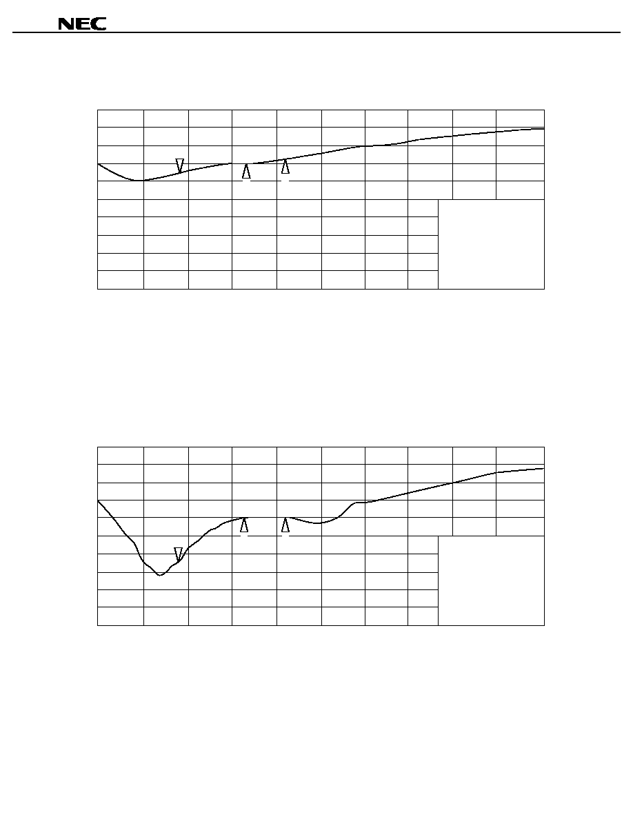
1
1:
2:
3:
≠17.37 dB
0.95 GHz
≠15.07 dB
1.7 GHz
≠13.41 dB
2.15 GHz
0
≠25
≠50
START 0.050 000 000 GHz
STOP 5.050 000 000 GHz
Ferquency f (GHz)
INPUT RETURN LOSS vs. FREQUENCY
log MAG
5 dB/div.
Input Retur
n Loss RL
in
(dB)
1
1:
2:
3:
≠32.13 dB
0.95 GHz
≠19.73 dB
1.7 GHz
≠19.68 dB
2.15 GHz
0
≠25
≠50
START 0.050 000 000 GHz
STOP 5.050 000 000 GHz
Frequency f (GHz)
OUTPUT RETURN LOSS vs. FREQUENCY
log MAG
5 dB/div.
Output Retur
n Loss RL
out
(dB)
2
3
2
3
Data Sheet P14268EJ2V0DS00
7
µ
µ
µ
µ
PG181GR
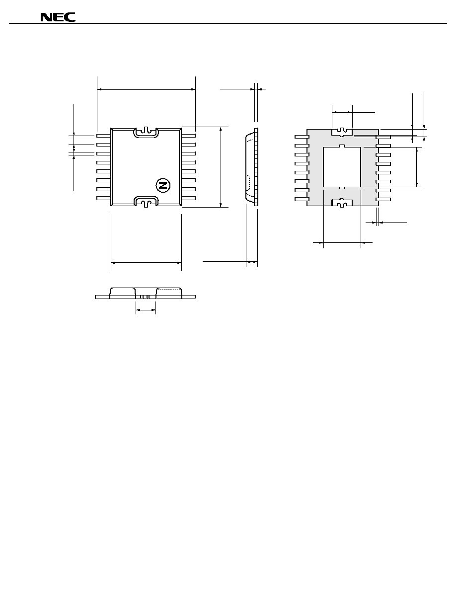
PACKAGE DIMENSIONS
16 PIN HTSSOP (Unit: mm)
(1.5)
5.2 ±0.2
0.9 ±0.2
5.5 ±0.3
0.20 ±0.10
6.4 ±0.3
9
16
8
1
(Bottom View)
0.65 ±0.1
0.20 ±0.10
(0.4)
(2.7)
(0.5)
(1.8)
(0.1)
(2.5)

Data Sheet P14268EJ2V0DS00
8
µ
µ
µ
µ
PG181GR
RECOMMENDED SOLDERING CONDITIONS
This product should be soldered under the following recommended conditions. For soldering methods and
conditions other than those recommended below, contact your NEC sales representative.
Soldering Method
Soldering Conditions
Recommended Condition
Symbol
Infrared Reflow
Package peak temperature: 235 ∞C or below
Time: 30 seconds or less (at 210 ∞C)
Count: 3, Exposure limit: None
Note
IR35-00-3
VPS
Package peak temperature: 215 ∞C or below
Time: 40 seconds or less (at 200 ∞C)
Count: 3, Exposure limit: None
Note
VP15-00-3
Wave Soldering
Soldering bath temperature: 260 ∞C or below
Time: 10 seconds or less
Count: 1, Exposure limit: None
Note
WS60-00-1
Partial Heating
Pin temperature: 300 ∞C
Time: 3 seconds or less (per side of device)
Exposure limit: None
Note
≠
Note After opening the dry pack, keep it in a place below 25 ∞C and 65 % RH for the allowable storage period.
Caution Do not use different soldering methods together (except for partial heating).
For details of recommended soldering conditions for surface mounting, refer to information document
SEMICONDUCTOR DEVICE MOUNTING TECHNOLOGY MANUAL (C10535E).

Data Sheet P14268EJ2V0DS00
9
µ
µ
µ
µ
PG181GR
[MEMO]

Data Sheet P14268EJ2V0DS00
10
µ
µ
µ
µ
PG181GR
[MEMO]

Data Sheet P14268EJ2V0DS00
11
µ
µ
µ
µ
PG181GR
[MEMO]

µ
µ
µ
µ
PG181GR
CAUTION
The Great Care must be taken in dealing with the devices in this guide.
The reason is that the material of the devices is GaAs (Gallium Arsenide), which is
designated as harmful substance according to the law concerned.
Keep the law concerned and so on, especially in case of removal.
∑
The information in this document is subject to change without notice. Before using this document, please
confirm that this is the latest version.
∑
No part of this document may be copied or reproduced in any form or by any means without the prior written
consent of NEC Corporation. NEC Corporation assumes no responsibility for any errors which may appear in
this document.
∑
NEC Corporation does not assume any liability for infringement of patents, copyrights or other intellectual property
rights of third parties by or arising from use of a device described herein or any other liability arising from use
of such device. No license, either express, implied or otherwise, is granted under any patents, copyrights or other
intellectual property rights of NEC Corporation or others.
∑
Descriptions of circuits, software, and other related information in this document are provided for illustrative
purposes in semiconductor product operation and application examples. The incorporation of these circuits,
software, and information in the design of the customer's equipment shall be done under the full responsibility
of the customer. NEC Corporation assumes no responsibility for any losses incurred by the customer or third
parties arising from the use of these circuits, software, and information.
∑
While NEC Corporation has been making continuous effort to enhance the reliability of its semiconductor devices,
the possibility of defects cannot be eliminated entirely. To minimize risks of damage or injury to persons or
property arising from a defect in an NEC semiconductor device, customers must incorporate sufficient safety
measures in its design, such as redundancy, fire-containment, and anti-failure features.
∑
NEC devices are classified into the following three quality grades:
"Standard", "Special", and "Specific". The Specific quality grade applies only to devices developed based on a
customer designated "quality assurance program" for a specific application. The recommended applications of
a device depend on its quality grade, as indicated below. Customers must check the quality grade of each device
before using it in a particular application.
Standard: Computers, office equipment, communications equipment, test and measurement equipment,
audio and visual equipment, home electronic appliances, machine tools, personal electronic
equipment and industrial robots
Special: Transportation equipment (automobiles, trains, ships, etc.), traffic control systems, anti-disaster
systems, anti-crime systems, safety equipment and medical equipment (not specifically designed
for life support)
Specific: Aircraft, aerospace equipment, submersible repeaters, nuclear reactor control systems, life
support systems or medical equipment for life support, etc.
The quality grade of NEC devices is "Standard" unless otherwise specified in NEC's Data Sheets or Data Books.
If customers intend to use NEC devices for applications other than those specified for Standard quality grade,
they should contact an NEC sales representative in advance.
M7 98. 8