 | –≠–ª–µ–∫—Ç—Ä–æ–Ω–Ω—ã–π –∫–æ–º–ø–æ–Ω–µ–Ω—Ç: UPG2012TB | –°–∫–∞—á–∞—Ç—å:  PDF PDF  ZIP ZIP |
FEATURES
NEC's
º
W SINGLE CONTROL
L-BAND SPDT SWITCH
UPG2012TB
California Eastern Laboratories
APPLICATIONS
∑ L-band digital cellular or cordless handsets
∑ PCS, W-LAN, WLL and Bluetooth
TM
∑ Short Range Wireless
NEC's UPG2012TB is a single control GaAs MMIC L-band
SPDT (Single Pole Double Throw) switch for mobile phone
and L-band applications.
This device can operate from 0.5 to 2.5 GHz, with low inser-
tion loss and high isolation.
This device is housed in a 6-pin super minimold package,
suitable for high-density surface mounting.
DESCRIPTION
∑ SUPPLY VOLTAGE:
V
DD
= 2.7 to 3.0 V (2.8 V TYP.)
∑ SWITCH CONTROL VOLTAGE:
V
cont (H)
= 2.7 to 3.0 V (2.8 V TYP.)
V
cont (L)
=
-
0.2 to +0.2 V (0 V TYP.)
∑ LOW INSERTION LOSS:
L
INS1
= 0.27 dB TYP. @ f = 0.5 to 1.0 GHz, V
DD
= 2.8 V, V
cont
= 2.8 V/0 V
L
INS2
= 0.30 dB TYP. @ f = 2.0 GHz, V
DD
= 2.8 V, V
cont
= 2.8 V/0 V
L
INS3
= 0.35 dB TYP. @ f = 2.5 GHz, V
DD
= 2.8 V, V
cont
= 2.8 V/0 V
(Reference value)
∑ HIGH ISOLATION:
ISL
1
= = 28 dB TYP. @ f = 0.5 to 2.0 GHz, V
DD
= 2.8 V, V
cont
= 2.8 V/0 V
ISL
2
= 25 dB TYP. @ f = 2.5 GHz, V
DD
= 2.8 V, V
cont
= 2.8 V/0 V
(Reference value)
∑ HIGH-DENSITY SURFACE MOUNTING:
6-pin super minimold package (2.0
◊
1.25
◊
0.9 mm)
Part Number
Package
Marking
Supplying Form
UPG2012TB-E3
6-pin super minimold
G3A
∑
Embossed tape 8 mm wide
∑
Pin 1, 2, 3 face the perforation side of the tape
∑
Qty 3 kpcs/reel
ORDERING INFORMATION
Remark
To order evaluation samples, contact your nearby sales offi ce.
Part number for sample order: UPG2012TB
Caution
Observe precautions when handling because these devices are sensitive to electrostatic discharge.
UPG2012TB
ABSOLUTE MAXIMUM RATINGS
(T
A
= 25∞C, unless otherwise specifi ed)
RECOMMENDED OPERATING RANGE
(T
A
= 25∞C, unless otherwise specifi ed)
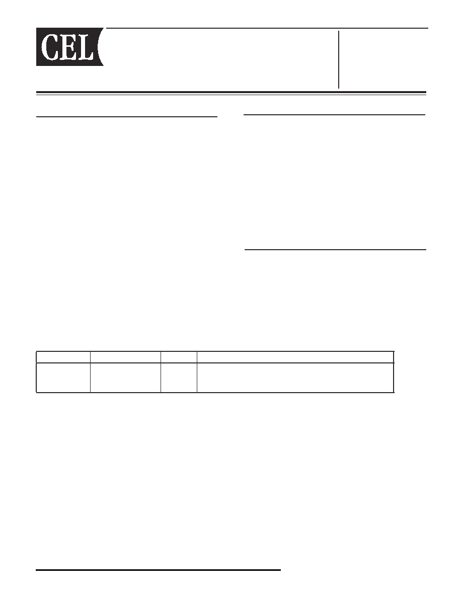
Pin No.
Pin Name
1
OUTPUT1
2
GND
3
OUTPUT2
4
V
Cont
5
INPUT
6
V
DD
TRUTH TABLE
Vcont
INPUT-OUTPUT1
INPUT-OUTPUT2
Low
OFF
ON
High
ON
OFF
PIN CONNECTIONS AND INTERNAL BLOCK DIAGRAM
Parameter
Symbol
Ratings
Unit
Supply Voltage
V
DD
+6.0
V
Switch Control Voltage
V
cont
+6.0
V
Input Power
P
in
+26
dBm
Power Dissipation
P
D
150
Note
mW
Operating Ambient Temperature
T
A
-
45 to +85
∞
C
Storage Temperature
T
stg
-
55 to +150
∞
C
Parameter
Symbol
MIN.
TYP.
MAX.
Unit
Switch Voltage
V
DD
2.7
2.8
3.0
V
Switch Control Voltage (H)
V
cont (H)
2.7
2.8
3.0
V
Switch Control Voltage (L)
V
cont (L)
-
0.2
0
0.2
V
Note
Mounted on double-sided copper-clad 50
◊
50
◊
1.6 mm epoxy glass PWB, T
A
= +85
∞
C
(Top View)
3
2
1
6
5
4
G3A
(Top View)
3
2
1
(Bottom View)
4
5
6
4
5
6
3
2
1
ELECTRICAL CHARACTERISTICS
(T
A
= +25
∞
C, V
DD
= 2.8 V, V
cont
= 2.8 V/0 V, DC blocking capacitors = 56 pF, unless otherwise specifi ed)
STANDARD CHARACTERISTICS FOR REFERENCE
(T
A
= +25
∞
C, V
DD
= 2.8 V, V
cont
= 2.8 V/0 V, DC blocking capacitors = 56 pF, unless otherwise specifi ed)
Note
P
in (0.1 dB)
is the measured input power level when the insertion loss increases 0.1 dB more than that of linear
range.
Caution It is necessary to use DC blocking capacitors with the device.
The value of DC blocking capacitors should be chosen to accommodate the frequency of operation,
bandwidth, switching speed and the condition with actual board of your system. The range of recommended
DC blocking capacitor value is less than 100 pF.
UPG2012TB
Parameter
Symbol
Test Conditions
MIN.
TYP.
MAX.
Unit
Insertion Loss1
L
INS1
f = 0.5 to 1.0 GHz
-
0.27
0.50
dB
Insertion Loss2
L
INS2
f = 2.0 GHz
-
0.30
0.50
dB
Isolation1
ISL1
f = 0.5 to 2.0 GHz
24
28
-
dB
Input Return Loss
RL
in
f = 0.5 to 2.5 GHz
15
20
-
dB
Output Return Loss
RL
out
f = 0.5 to 2.5 GHz
15
20
-
dB
0.1 dB Gain Compression
Input Power
Note
P
in(0.1 dB)
f = 2.0 GHz
+17.5
+20.5
-
dBm
Supply Current
I
DD
-
50
100
µ
A
Switching Control Current
I
cont
-
4
20
µ
A
Parameter
Symbol
Test Conditions
MIN.
TYP.
MAX.
Unit
Insertion Loss3
L
INS3
f = 2.5 GHz
-
0.30
-
dB
Isolation2
ISL2
f = 2.5 GHz
-
25
-
dB
1 dB Gain Compression
Input Power
Note
P
in(1 dB)
f = 2.0 GHz
-
+24.0
-
dBm
Switching Control Speed
t
SW
-
300
-
ns
4-277
UPG2012TB
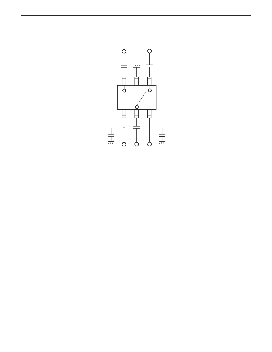
EVALUATION CIRCUIT
(V
DD
= 2.8 V, V
cont
= 2.8 V/0 V, DC blocking capacitors = 56 pF)
The application circuits and their parameters are for reference only and are not intended for use in actual design-ins.
4
5
6
OUTPUT1
OUTPUT2
56 pF
56 pF
3
2
1
V
DD
V
cont
INPUT
56 pF
1 000 pF
1 000 pF
UPG2012TB
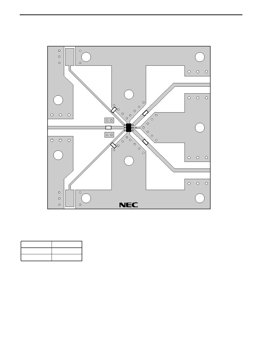
ILLUSTRATION OF THE TEST CIRCUIT ASSEMBLED ON EVALUATION BOARD
USING THE NEC EVALUATION BOARD
Symbol
Values
C1, C2, C3
56 pF
C4, C5
1 000 pF
6pin SMM SPDT SW
Vc1
Vc2
IN
OUT 1
OUT 2
C1
C1
C3
C5
C1
C2
C4
C1
C2
C2
V
DD
OUTPUT1
INPUT
OUTPUT2
V
cont
G3A
UPG2012TB
UPG2012TB
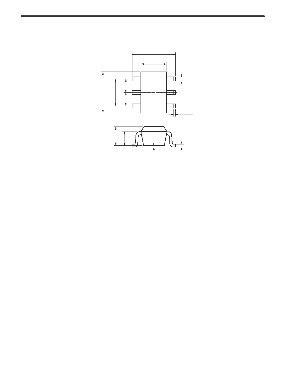
PACKAGE DIMENSIONS
6-PIN SUPER MINIMOLD (UNIT: mm)
0.9±0.1
0.7
0≠0.1
0.15
+0.1 -0.05
0.2
+0.1 ≠0.05
2.0±0.2
1.3
0.65
0.65
1.25±0.1
2.1±0.1
0.1 MIN.
UPG2012TB
RECOMMENDED SOLDERING CONDITIONS
This product should be soldered and mounted under the following recommended conditions. For soldering methods and
conditions other than those recommended below, contact your nearby sales offi ce.
Soldering Method
Soldering Conditions
Condition Symbol
Infrared Refl ow
Peak temperature (package surface temperature)
: 260
∞
C or below
Time at peak temperature
: 10 seconds or less
Time at temperature of 220
∞
C or higher
: 60 seconds or less
Preheating time at 120 to 180
∞
C :
120
±
30 seconds
Maximum number of refl ow processes
: 3 times
Maximum chlorine content of rosin fl ux (% mass)
: 0.2%(Wt.) or below
IR260
VPS
Peak temperature (package surface temperature)
: 215
∞
C or below
Time at temperature of 200
∞
C or higher
: 25 to 40 seconds
Preheating time at 120 to 150
∞
C
: 30 to 60 seconds
Maximum number of refl ow processes
: 3 times
Maximum chlorine content of rosin fl ux (% mass)
: 0.2%(Wt.) or below
VP215
Wave Soldering
Peak temperature (molten solder temperature)
: 260
∞
C or below
Time at peak temperature
: 10 seconds or less
Preheating temperature (package surface temperature) : 120
∞
C or below
Maximum number of fl ow processes
: 1 time
Maximum chlorine content of rosin fl ux (% mass)
: 0.2%(Wt.) or below
WS260
Partial Heating
Peak temperature (pin temperature)
: 350
∞
C or below
Soldering time (per side of device)
: 3 seconds or less
Maximum chlorine content of rosin fl ux (% mass)
: 0.2%(Wt.) or below
HS350
Caution Do not use different soldering methods together (except for partial heating).
Life Support Applications
These NEC products are not intended for use in life support devices, appliances, or systems where the malfunction of these products can reasonably be expected
to result in personal injury. The customers of CEL using or selling these products for use in such applications do so at their own risk and agree to fully indemnify
CEL for all damages resulting from such improper use or sale.
A Business Partner of NEC Compound Semiconductor Devices, Ltd.
02/19/2004