 | –≠–ª–µ–∫—Ç—Ä–æ–Ω–Ω—ã–π –∫–æ–º–ø–æ–Ω–µ–Ω—Ç: CB-C9VX | –°–∫–∞—á–∞—Ç—å:  PDF PDF  ZIP ZIP |

NEC Electronics Inc.
CB-C9VX
3.3-Volt, 0.35-Micron
Cell-Based CMOS ASIC
January 1998
Preliminary
A12411EU2V0DS01
OpenCAD is a registered trademark of NEC Electronics Inc.
Description
NEC's CB-C9VX CMOS cell-based ASIC family facilitates
the design of complete cell-based silicon systems com-
posed of user-defined logic, complex macro functions
such as microprocessors, intelligent peripherals, analog
functions, and compiled memory blocks on an area-
efficient die size due to a much higher gate density.
The CB-C9VX cell-based ASIC series is the second
generation of a 0.35-micron (0.27-micron effective) sili-
con gate CMOS process with silicidation. This advanced
process greatly reduces the number of contacts per cell,
leading to library elements optimized on area and speed
with a 2.0-3.3V power supply. CB-C9VX achieves 17.5K
gates/mm
2
, which allows designs with higher gate counts
on a smaller area, compared to the CB-C9 series. Replac-
ing the metal2 routing within each cell with poly-silicon and
tightening the metal pitch has resulted in a much higher
density (smaller grid size) and improved routability. For
this technology, the Titanium-Silicide process results in
excess of 50% reduced power consumption per cell,
compared to 0.35-micron 3.3V technologies. The ultra-
high integration, super-high speed, and low power con-
sumption of this technology meets today's high-perfor-
mance application demands.
Fully supported by NEC's sophisticated OpenCAD
Æ
design framework, CB-C9VX maximizes design quality
and flexibility while minimizing ASIC design time. NEC's
OpenCAD system combines popular third-party design
tools with proprietary NEC tools, including advanced
floorplanner and clock tree synthesis tools.
5V-Tolerant Interface
CB-C9VX supports both 3.3V and 5V-tolerant signaling.
The 5V-tolerant buffers enable CB-C9VX devices to
communicate with 5V TTL signals while protecting the
ASIC. If 5V-tolerant buffers are not required, 3.3V buffers
may be substituted, thus increasing the die area available
for logic.
CB-C9VX Family Features
∑ 0.35-micron (drawn), Ti-Silicide CMOS technology
∑ Smaller metal pitch and modification of second layer metal
∑ 2.0-3.3V operation
∑ Twenty-six base sizes, each with DLM and TLM options
∑ Level shifter I/O: 3.3V external to 2.5V internal
∑ Three pad ring options for high gate-to-pad ratio
∑ PCI buffer, including 66 MHz PCI
∑ GTL+, AGP, SSTL, LVTTL, HSTL, pECL buffer support
∑ Ultra-low power dissipation: 0.3 µW/MHz/gate (3.3V)
∑ Extensive macro selection (CPUs, peripherals, analog)
∑ Datapath compiler for various ALUs, multipliers, adders
∑ Memory compiler for various types of memory blocks
∑ Extensive package support: PQFP, BGA, TBGA, CSP
∑ Automatic clock skew control by clock tree synthesis
∑ Popular, third-party CAE tools
CB-C9VX Family Benefits
∑ Ultra-high density cell structure
∑ >100% increase in gate density, improved routability
∑ Super high-speed at low power supply
∑ Flexible base sizes to best fit design needs
∑ Flexible interfacing to different signal voltages
∑ Minimum device cost for high I/O requirement
∑ PCI support compliant with latest PCI specification
∑ High-speed I/F to memory and processor buses
∑ Ideally suited for hand-held applications
∑ Advanced system-on-silicon design
∑ Speed and area-effective memory modules
∑ Area-effective memory integration on-chip
∑ The latest package requirements
∑ Minimal on-chip clock skew
∑ Smooth design flow from customer design to silicon
Table 1. CB-C9VX Family Features and Benefits
CB-C9VX
2
Integration and Performance
Gate complexities up to 1.74M usable gates can be
integrated on the largest of more than 20 step sizes, each
routable with 2- or 3-metal layers. This gives enough
flexibility to optimally fit design needs. Modifications in the
second layer metal and the metal pitch have resulted in
much higher gate density and improved routability.
The family offers an extensive library of primitive
macrofunctions characterized for 3.3V operation (2.0V
operation in the future). Each of these blocks has several
different drive strengths, allowing the synthesis tool to
select the most suitable block for the required internal
load. This generally reduces the design overhead without
influencing design performance. The internal gate delay
for a two-input NAND gate is 86* picoseconds (ps),
(F/O=1, L=0mm, 3.3V operation) and under loaded con-
ditions 183.1* ps (F/O=2, L=typ, 3.3V operation).
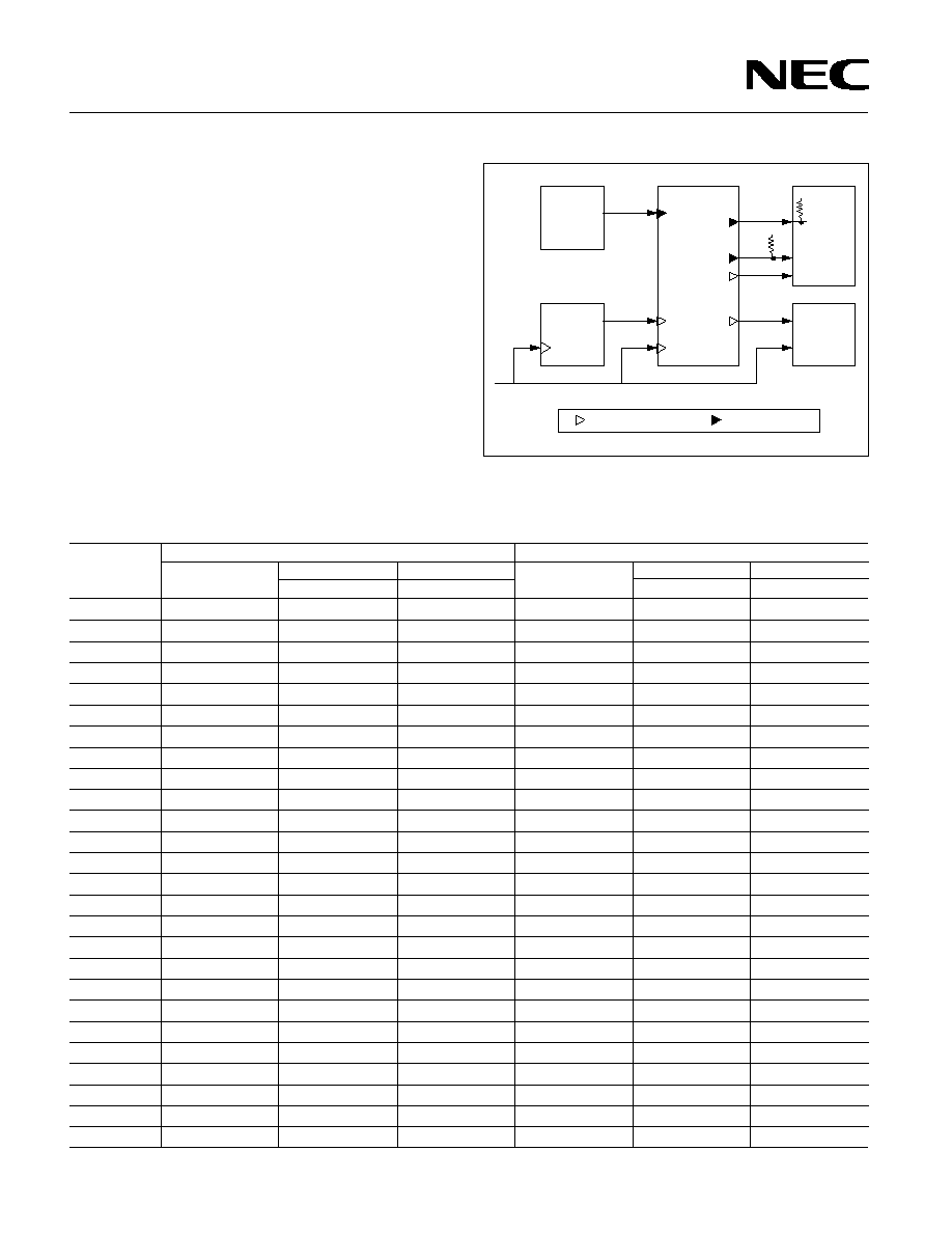
Figure 1. CB-C9VX 5V Interfacing
5V
Device
3V
Device
CB-C9
ASIC
(3V)
3V
Device
5V
Device
CMOS I/F
TTL I/F
3V Interface Block
5V Interface Block
3V CLK
CB-C9VX
ASIC
(3V)
Table 2. CB-C9VX Step Sizes (Preliminary)
Only 3V I/F Buffer
3V, 5V I/F Buffer
2LM
3LM
2LM
3LM
Step Size
Raw Grid [K]
Gate Counts [K]
Gate Count [K]
Raw Grid [K]
Gate Counts [K]
Gate Counts [K]
B60
527.5
89.7
131.9
397.7
67.6
99.4
C02
706.5
117.3
174.1
555.8
92.3
137.0
C40
869.5
142.0
212.1
721.0
117.7
175.8
C78
1101.2
176.3
265.4
915.4
146.5
220.6
D01
1223.5
194.1
293.3
1037.3
164.6
248.6
D26
1378.4
216.5
328.4
1177.0
184.9
280.4
D52
1546.3
240.5
366.2
1339.3
208.3
317.2
D90
1812.8
278.0
425.8
1579.5
242.3
371.0
E16
2011.0
305.6
469.8
1746.9
265.5
408.1
E54
2294.7
344.7
532.4
2027.5
304.5
470.4
E80
2488.9
371.1
575.0
2235.8
333.4
516.5
F18
2814.7
415.1
646.0
2531.8
373.3
581.1
F44
3056.8
447.4
698.5
2732.3
399.9
624.3
F70
3271.7
475.8
744.9
2971.3
432.1
676.5
G08
3639.3
524.1
823.8
3320.0
478.1
751.5
G34
3867.7
553.8
872.6
3545.9
507.7
800.0
G72
4274.0
606.2
959.1
3920.2
556.0
879.7
H10
4683.4
658.5
1045.7
4315.6
606.8
963.6
H49
5105.6
711.9
1134.6
4741.2
661.1
1053.6
H87
5539.2
766.3
1225.4
5166.0
714.7
1142.8
J26
5951.5
817.6
1311.4
5608.2
770.4
1235.7
J51
6263.0
856.1
1376.1
5873.0
802.8
1290.4
K15
7089.4
957.2
1546.9
6679.8
901.9
1457.6
K92
8037.5
1071.7
1741.5
7607.5
1014.3
1648.3
M97
10898.6
1408.5
2320.7
10424.5
1347.2
2219.8
P63
13509.1
1706.8
2841.1
13009.0
1643.6
2735.9
Grid/gate conversion ratio = 3 grids/gate
*
Preliminary

3
CB-C9VX
To meet today's high-speed demands, high-performance
I/O macros are mandatory. CB-C9VX supports macros
such as GTL+, SSTL, LVTTL, pECL, and HSTL for fast,
low power data transfer, PLLs to synchronize on-chip
system clocks, and PCI signaling standards and AGP for
graphics applications. Also, CB-C9VX offers a variety of
macro functions to be incorporated on a single chip.
These macro functions include CPU cores, peripheral
devices, RAM/ROM and datapath macros and functions
that enables designers to create systems on silicon.
Moreover, level shifters (connected between 3.3V exter-
nal and 2.5V internal) provide low power consumption and
flexible interfacing to different signal voltages making
correspondence.
Low Power Consumption
NEC's CB-C9VX Titanium-Silicide process features
exceptionally low power dissipation to facilitate super-
high-speed operation without the need for costly package
options. The process also drastically increases battery
life for hand-held applications. The new ASIC family
dissipates power at 0.3 µW/MHz/gate (@3.3V).
Test Simplification Design
To easily test the logical circuit of 2.7M gate large-scale,
CB-C9VX allows use of Scan and Boundary Scan for logic
area, BIST for memory macros, and direct-accessed test
bus architecture for core macros.
System on Silicon
NEC offers a wide selection of CPU/MCU cores, industry-
standard intelligent peripheral macros, and compilable
RAM/ROM blocks and datapath macros as well as analog
functions in hard macro form that can be integrated onto
a single CB-C9VX chip. Including such macro functions
in an ASIC design makes it possible to achieve a high level
of integration, performance, and system security.
The range of NEC's proprietary 32-bit RISC CPUs
includes V830TM, V851TM, V853TM which has the V810
core and a 16-bit external data bus, and also ARM7TDMI.
An upgraded high-speed version of the popular 16-bit
CPU V30MXTM operates at clock speeds of 33 MHz at
3.3V and offers an improved 286-compatible address
pipelining and uses a 24-bit address bus. Other specific
cores can be implemented on request.
Embedded macro functions are easy to place, route, and
simulate. Because these macros are derived from NEC's
standard parts, they have fully characterized parameters
and can be tested with standard test vectors to ensure full
functionality and reliability.
NEC's test bus architecture allows complete system
simulation, production testing of the internal circuits of
the macro functions, and seamless embedded CPU core
emulation. The CPU may be connected externally and
can be replaced by an in-circuit emulator (ICE). All this is
performed with only two dedicated test control pins.
V810, V830, V851, V853, and V30MX are trademarks of
NEC Corporation.
CB-C9VX
4
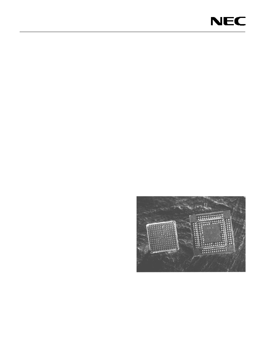
Figure 2. FBGA photo
actual load conditions but also of the logic cells input
slopes. NEC developed this delay modeling method to
enable a converging design flow and to minimize design
iterations.
Test Support
The CB-C9VX family supports automatic test generation
through a scan test methodology, which allows higher
fault coverage, easier testing and faster development
time. This includes internal scan as well as boundary
scan. NEC also offers optional built-in-self-test (BIST)
architecture for RAM testing. Test of embedded
megamacros is supported from NEC's test bus concept,
which allows the use of predefined test pattern sets, for
example, for integrated core macros.
Packaging
NEC offers a wide variety of over 60 package types. The
CB-C9VX family can be packaged in NEC's most popular
surface-mount and through-hole packages. These in-
clude plastic quad flat packs (PQFPs) with optional heat
spreader and pin counts in the range from 160 to 304 pins.
Pin grid arrays (PGAs) with 364 or 528 pins and ball grid
array (BGA) packages with 256 to 692 ball contacts are
also supported. See Figure 2 for package photo.
CB-C9VX Applications
Major advantages of NEC's CB-C9VX ASIC family
include its ultra-high density, high speed, very low power
consumption and cost-effective memory and megamacro
integration.
These advantages support a wide range of applications.
For example, high-performance transmission and
switching systems, based on ATM technique, may take
advantage of high speed, high-integration density and
high-performance memory integration. High-end hand-
held applications such as PDAs or mobile communication
equipment make use of low power and the capability of
global system integration, including powerful micropro-
cessor cores that result in small system cases. Future
high-end consumer products such as digital TV set-top
boxes need system-on-silicon integration to allow cost-
effective mass production. High-end chipsets for
engineering workstations (EWS) or graphic PC subsystems
need very high performance combined with cost-effective
packaging solutions. With its very low power consump-
tion and densely packed gates, NEC's CB-C9VX family
enables the usage of more cost-effective packaging solu-
tions.
CAD Support
The CB-C9VX family ASICs are completely supported by
NEC's OpenCAD design environment, a unified front-to-
back-end design package that allows designers to mix
and match tools from the industry's most popular third-
party vendors and from NEC's offering of powerful propri-
etary software tools. These tools perform schematic
capture, logic synthesis, floorplanning, logic and timing
simulation layout, design and circuit rule check, and
memory compilation. The company's proprietary clock
tree synthesis tool can be used to automatically buffer the
clock lines as needed to minimize clock skew, essential
for high-speed designs.
The library elements of NEC's CB-C9VX family are
modeled in a nonlinear way using table look-up methods.
This allows the most accurate timing verification through-
out synthesis, estimated timing simulation and sign-off
timing simulation as it includes not only the influence of
5
CB-C9VX
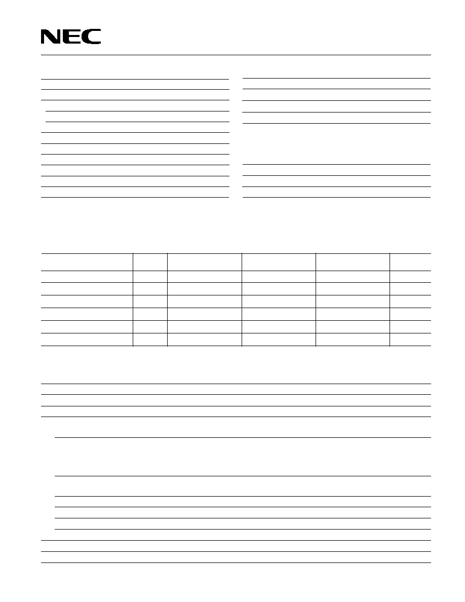
Absolute Maximum Ratings
Power supply voltage, V
DD
-0.5 to +4.6V
I/O voltage, V
I
3V input buffer (at V
I
< V
DD
+0.5V)
-0.5 to +4.6V
3.3V fail-safe input buffer (at V
I
< V
DD
+0.5V)
-0.5 to +4.6V
5V-tolerant buffer (at V
I
< V
DD
+3.0V)
-0.5 to +4.6V
Output voltage, V
O
3V buffer (at V
O
< V
DD
+0.5V)
-0.5 to +4.6V
5V-tolerant buffer (at V
O
< V
DD
+3.0V)
-0.5 to +4.6V
Latch-up current, I
LATCH
>1 A (typ)
Operating temperature, T
OPT
-40 to +85∞C
Storage temperature, T
STG
-65 to +150∞C
Caution: Exposure to absolute maximum ratings for extended periods may affect
device reliability; exceeding the ratings could cause permanent damage. The device
should not be operated outside the recommended operating conditions.
Power Consumption
Description
Limits
Unit
2-input NAND (F302: F/O=0, L=0)
0.37
µW/MHz
2-input NAND (F302: F/O=2, L=typ)
0.63
µW/MHz
Caution: Exposure to absolute maximum ratings for extended periods may affect
device reliability; exceeding the ratings could cause permanent damage. The device
should not be operated outside the recommended operating conditions.
Input/Output Capacitance
(V
DD
= V
I
= 0V; f = 1 MHz)
Terminal
Symbol
Typ
Max
Unit
Input
C
IN
10
20
pF
Output
C
OUT
10
20
pF
I/O
C
I/O
10
20
pF
(1)
Values include package pin capacitance
Recommended Operating Conditions
(V
DD
= 3.3V ± 0.3V; T
J
= 0∞C to +125∞C)
3.3V Buffer
5V-Tolerant
3.3V PCI
Parameter
Symbol
Min
Max
Min
Max
Min
Max
Unit
I/O power supply voltage
V
DD
3.0
3.6
3.0
3.6
3.0
3.6
V
Junction temperature
T
J
≠0
+125
≠0
+125
≠0
+125
∞C
High-level input voltage
V
IH
2.0
V
DD
2.0
V
DD
0.5 V
DD
V
DD
+0.5
V
Low-level input voltage
V
IL
0
0.8
0
0.8
≠0.5
0.3 V
DD
V
Input rise/fall time
t
R
, t
F
0
200
0
200
0
200
ns
Input rise/fall time, Schmitt
t
R
, t
F
0
10
0
10
0
200
ms
AC Characteristics
(V
DD
= 3.3V ± 0.3V; T
J
= 0∞C to +125∞C)
Parameter
Symbol
Min
Typ
Max
Unit
Conditions
Toggle frequency
f
TOG
880
MHz
D-F/F; F/O = 2 mm, L = 0 mm
Delay time
2-input NAND (F322)
t
PD
49.8
76.1
113.2
ps
F/O = 1; L = 0 mm
t
PD
76.6
113.8
169.9
ps
F/O = 2; L = typ
Flip-flop (F611NQ)
t
PD
321.4
497.4
776.1
ps
F/O = 1; L = 0 mm
t
PD
354.2
549.6
860.0
ps
F/O = 2; L = typ
t
SETUP
490
ps
--
t
HOLD
390
ps
--
Input buffer (FI01)
t
PD
107.4
155.6
221.9
ps
F/O = 1; L = 0 mm
t
PD
126.7
175.5
252.0
ps
F/O = 2; L = typ
Output buffer (12 mA) 3.3V
t
PD
454.5
675.5
1021
ps
C
L
= 0 pF
Output buffer (12 mA) 3.3V
t
PD
1624
2375
3525
ps
C
L
= 50 pF
Output buffer (6 mA) 5V-tolerant
t
PD
957
1393
2078
ps
C
L
= 0 pF
Output buffer (6 mA) 5V-tolerant
t
PD
2508
3650
5408
ps
C
L
= 50 pF
Output rise time (9 mA)
t
R
1708
2165
2994
ps
C
L
= 15 pF; 10-90%
Output fall time (9 mA)
t
F
1082
1522
2381
ps
C
L
= 15 pF; 10-90%