 | –≠–ª–µ–∫—Ç—Ä–æ–Ω–Ω—ã–π –∫–æ–º–ø–æ–Ω–µ–Ω—Ç: CMOS-9 | –°–∫–∞—á–∞—Ç—å:  PDF PDF  ZIP ZIP |
July 1997
NEC Electronics Inc.
A12634EU1V0DS00
CMOS-9
3.3-VOLT, 0.35-MICRON
CMOS GATE ARRAYS
Description
NEC's CMOS-9 gate array family provides designers
with the performance capabilities and features required
to develop devices for high-speed computer and
communications systems. NEC combines the highest
performance 0.35-micron drawn gate length (Leff=0.27
micron) 2- and 3-level metal CMOS technology with an
extensive family of interface macros to support very
high-speed system clocks. The high performance I/O
macros including GTL, HSTL, and pECL are under
development. PCI signaling standards are also
supported including 3.3V 66 MHz PCI.
This technology is enhanced by a set of advanced
features including phase-locked loops, clock tree
synthesis, and high-speed memory.
The CMOS-9 gate array family of 3.3-volt devices
consists of 20 masters, offered in densities of 190K raw
gates to 2 million raw gates. Usable gates range from
76K to 1.2 million used gates.
The gate array family is supported by NEC's OpenCAD
Æ
design system; a mixture of popular third-party CAE
tools, and proprietary NEC tools. NEC proprietary tools
include the GALET floorplanner which helps reduce
design cycle time and improve design performance,
clock tree synthesis for clock skew minimization, and
table look-up delay calculator for accurate delay
calculation.
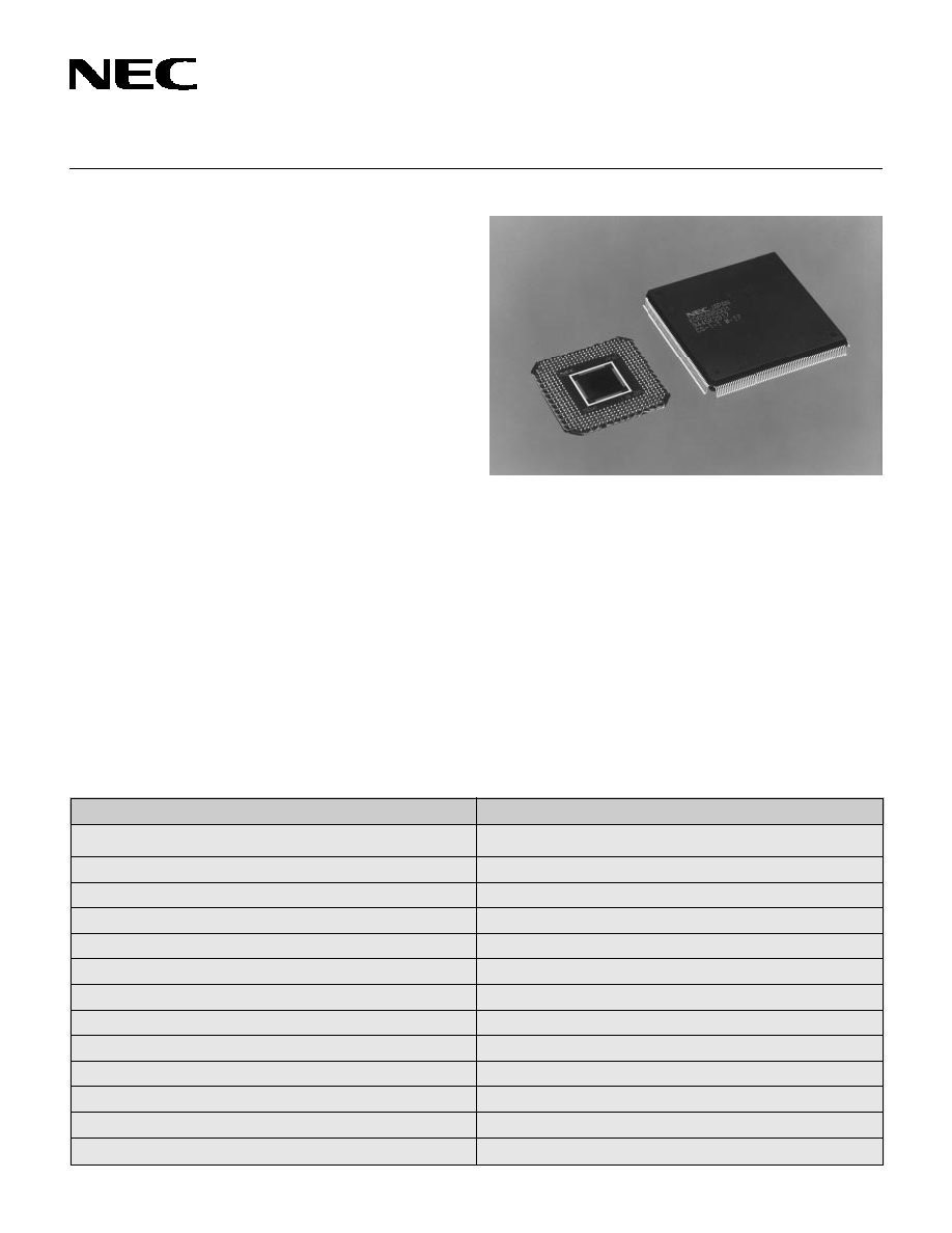
Figure 1. CMOS-9 Package Examples; BGA and QFP
Table 1. CMOS-9 Series Features and Benefits
CMOS-9 Series Features
∑ 0.35-micron (drawn), 2 and 3-level metal CMOS technology
∑ Eighteen base arrays with raw gates from 190K to 1.5M
∑ Narrow pad pitch for maximum gate to pad ratio
∑ Pad counts from 300 to 1060 pads
∑ GTL, GTL+, pECL, and all four classes of HSTL
∑ Full range of 5V-protected I/O buffers
∑ PCI buffers including 3.3V 66 MHz PCI buffer
∑ Phase-Locked Loop (DPLL) macros in development
∑ Low power dissipation: 0.9 µW/MHz/gate
∑ Extensive package offering: PQFP, TQFP, BGA, TAB
∑ Clock Tree Synthesis tool automates clock tree design
∑ Floorplanner supplies layout information for resynthesis
∑ Popular, third-party CAE tools supported
CMOS-9 Series Benefits
∑ Delivers dense cell structure and high speed
∑ Provides many base sizes to give best fit to design needs
∑ Minimizes device cost
∑ Supports high I/O integration and wide system bus widths
∑ Interfaces to high speed memory and processor buses
∑ Allows interface with 5V logic while protecting 3.3V ASIC
∑ Supports signaling methods defined in PCI Spec 2.1
∑ Eliminates clock insertion delay, reduces total clock skew
∑ Provides low power consumption at high system clock rates
∑ Delivers customer-specific package requirements
∑ Minimizes on-chip clock skew for high performance
∑ Reduces design time and improves device performance
∑ Enables a smooth flow from customer design to silicon
CMOS-9 Applications
The CMOS-9 family is ideal for use in enterprise
systems, engineering workstations, telecommunications
switching and transmission systems, where extensive
integration and high speeds are primary design goals.
CMOS-9 is well-suited for designs requiring very high
integration (300K-600K gates, 400-600 pins), high
system speeds (100-200 MHz), and high performance
interface standards (HSTL, GTL). CMOS-9 is also well-
suited for lower power applications where high
performance is required. CMOS-9 is offered now at
3.3V and will be released at 2.5V in the future.
OpenCAD is a registered trademark of NEC Electronics Inc.
All non-NEC trademarks are the property of their respective owners.
CMOS-9
2
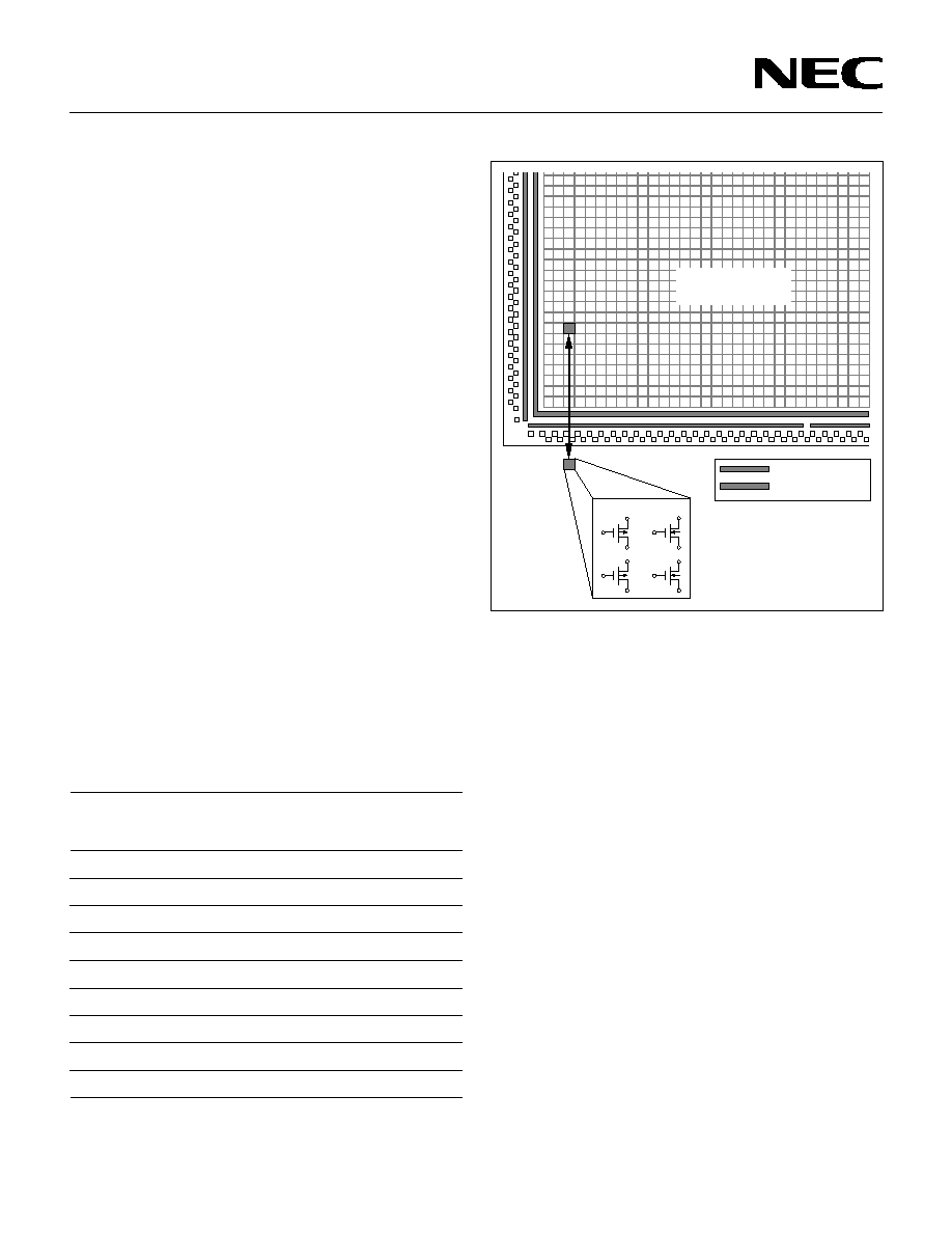
Array Architecture
The CMOS-9 gate array family is built with NEC's 0.35-
micron (drawn) channelless array architecture. As
shown in Figure 2, the array is divided into I/O and core
regions. The I/O region contains input and output
buffers. The core region contains the sea-of-gates array.
The CMOS-9 gate arrays architecture provides extra
flexibility for high performance system designs. As
shown in Figure 2, the arrays contain two power rails: a
3.3V rail, and a second power rail (V
DD2
) for special I/O
types.
The V
DD2
rail is used for interfaces such as HSTL where
a very low I/O power supply is required (1.4 to 1.6V). All
four classes of HSTL buffer are supported.
The V
DD2
rail may be separated into sections to allow
one device to support two or more busses requiring
special I/O voltages. Examples of spread I/O cells that
may use this V
DD
rail are HSTL and 5V PCI. Each
section can operate as an independent voltage zone,
and sections can be linked together to form common
voltage zones.
Core Architecture
The core region consists of an array of gates. Each gate
contains 2 n-channel and 2 p-channel MOS logic
transistors. One core gate is equivalent to one 2-input
NAND gate (L302). The logic transistors are sized to
offer a superior ratio of speed to silicon area.
Figure 2. CMOS-9 Power Rail Structure
(1) 2LM represents two-layer metal; 3LM represents three-layer metal.
(2) Actual gate utilization varies depending on circuit implementation.
Utilization is 40% for 2LM; 60% for 3LM.
Table 2. CMOS-9 Base Array Line-up
Device
(1)
Max Pads
(µPD659xx)
Available Usable Gates
(2)
Regular
Tight
2LM
3LM
Gates
2LM
3LM
Pitch
Pitch
06
26
190152
76061
114091
300
388
07
27
249948
99979
149969
340
444
08
28
317904
127162
190742
380
500
09
29
376740
150696
226044
412
540
10
30
462088
184835
277253
452
596
11
31
629824
251930
377894
524
692
13
33
805580
322232
483348
588
772
15
35
1076032
430413
645619
676
892
17
37
1545240
618096
927144
804
1060
Packaging and Test
CMOS-9 gate arrays support automatic test generation
through a scan-test methodology, which allows higher
fault coverage, easier testing and quicker development
time. NEC also offers optional BIST test structures for
RAM testing.
NEC offers advanced packaging solutions including Ball
Grid Arrays (BGA), Plastic Quad Flat Packs (PQFP),
Low Profile Plastic Quad Flat Packs (LQFP), Thin Plastic
Quad Flat Packs (TQFP), Pin Grid Arrays (PGA) and
advanced TAB technology.
Please contact your local NEC ASIC Design Center for a
listing of available master/package combinations.
Publications
This data sheet contains preliminary specifications,
package information, and operational data for the
C M O S - 9 g a t e a r r a y f a m i l y . A d d i t i o n a l d e s i g n
information will be available in NEC's CMOS-9 Block
Library and CMOS-9 Design Manual.
Contact your local NEC ASIC Design Center or the NEC
Literature Center for further ASIC design information;
see the back of this data sheet for locations and phone
numbers.
3.3V VDD Rail
VDD2
Core Region
P-Channel
N-Channel
3
CMOS-9
Power Consumption
Description
Limits
Unit
Internal gate
1.09
µW/MHz
Input buffer (FI01)
15.05
µW/MHz
Output buffer (FO01 @ 15 pF)
234
µW/MHz
Absolute Maximum Ratings
Power supply voltage, V
DD
≠0.5 to +4.6 V
Input voltage, V
I
3V Input buffer (at V
I
< V
DD
+ 0.5V)
-0.5 to 4.6 V
3V Fail-safe input buffer (at V
I
< V
DD
+ 0.5V)
-0.5 to 4.6 V
5V Input buffer (at V
I
< V
DD
+ 0.5V)
-0.5 to 6.6 V
Output voltage, V
O
3V Output buffer (at V
O
< V
DD
+ 0.5V)
-0.5 to 4.6 V
5V TTL Output buffer (at V
O
< V
DD
+ 3.0V)
-0.5 to 6.6 V
5V CMOS Output buffer (at V
O
< V
DD
+ 3.0V)
-0.5 to 6.6 V
Latch-up current, I
LATCH
>1 A (typ)
Operating temperature, T
OPT
-40 to +85∞C
Storage temperature, T
STG
-65 to +150∞C
AC Characteristics
V
DD
= 3.3V ± 0.3V; T
j
= -40 to +125∞C
Parameter
Symbol
Min
Typ
Max
Unit
Conditions
Toggle frequency (D-flip-flop)
f
TOG
670
MHz
F/O = 2, 5V
Delay time, 2-input NAND gate @ 5V
99
ps
F/O = 1; L = 0 mm
Standard gate (F302)
t
PD
150
ps
F/O = 2; L = 0.5 mm
84
ps
F/O = 1; L = 0 mm
Power gate (F322)
t
PD
119
ps
F/O = 2; L = 0.5 mm
Delay time, buffer
Input buffer (FI01)
t
PD
188
ps
F/O = 1; L = 0.5 mm
Input buffer (FI01)
t
PD
216
ps
F/O = 2; L = 0 mm
Output buffer (FO01)
t
PD
1.40
ns
C
L
= 15 pF
Output rise time (FO01)
t
R
2.35
ns
C
L
= 15 pF
Output fall time (FO01)
t
F
1.83
ns
C
L
= 15 pF
Caution:
Exposure to absolute maximum ratings for extended periods may
affect device reliability; exceeding the ratings could cause permanent
damage. The device should not be operated outside the recommended
operating conditions.
Recommended Operating Conditions
3.3V Interface 5V Interface
5V PCI 3.3V PCI
Block
Block
Level
Level
Parameter
Symbol
Min
Max
Min
Max
Min
Max
Min
Max
Unit
I/O Power supply voltage
V
DD
3.0
3.6
3.0
3.6
3.0
3.6
3.0
3.6
V
Junction temperature
T
J
-40
+125
-40
+125
-40
+125
-40
+125
∞C
High-level input voltage
V
IH
2.0
V
DD
2.0
5.5
2.0
V
CC
0.5V
CC
V
CC
V
Low-level input voltage
V
IL
0
0.8
0
0.8
0
0.8
0
0.3V
CC
V
Positive trigger voltage
V
P
1.5
2.7
2.2
2.55
--
--
--
--
V
Negative trigger voltage
V
N
0.6
1.4
0.84
1.01
--
--
--
--
V
Hysteresis voltage
V
H
1.1
1.5
1.36
1.54
--
--
--
--
V
Input rise/fall time
t
R
, t
F
0
200
0
200
0
200
0
200
ns
Input rise/fall time, Schmitt
t
R
, t
F
0
10
0
10
--
--
--
--
ns
Input/Output Capacitance
V
DD
= V
I
= 0 V; f = 1 MHz
Terminal
Symbol
MIn
Typ
Max
Unit
3V
4.0
6.0
Input
C
IN
pF
5V
8.0
10.0
3V
4.0
6.0
Output
C
OUT
pF
5V
8.0
10.0
3V
4.0
6.0
I/O
C
I/O
pF
5V
8.0
10.0
1) Values include package pin capacitance.
CMOS-9
4
DC Characteristics
V
DD
= 3.3V ± 0.3V; T
j
= -40 to +125∞C
Parameter
Symbol
Min
Typ
Max
Unit
Conditions
Quiescent current (µPD659xx)
(1)
-19, -39
I
L
7
1400
µA
V
I
= V
DD
or GND
-17, -37, -15, -35, -13, -33, -11, -31
I
L
4
800
µA
V
I
= V
DD
or GND
-10, -30, -09, -29, -08, -28
I
L
2
400
µA
V
I
= V
DD
or GND
-06, -26, -07, -27
I
L
1
200
µA
V
I
= V
DD
or GND
Off-state output leakage current
3V output buffer
I
OZ
±10
µA
V
O
= V
DD
or GND
5V-protected TTL buffer
I
OZ
±10
µA
V
O
= V
DD
or GND
Output short circuit current
(3)
I
OS
-250
mA
V
O
= GND
Input leakage current
(2)
Regular
I
I
±10
≠4
±10
µA
V
I
= V
DD
or GND
50 k
pull-up
I
I
36
89
165
µA
V
I
= GND
5 k
pull-up
I
I
284
654
1305
µA
V
I
= GND
50 k
pull-down
I
I
28
79
141
µA
V
I
= V
DD
Resistor values
50 k
pull-up
(4)
R
pu
21.8
37.1
83.1
k
5 k
pull-up
R
pu
2.8
5.0
10.6
k
50 k
pull-down
R
pu
25.6
41.9
105.8
k
Low-level output current (5V Interface block)
1 mA
I
OL
1
mA
V
OL
= 0.4 V
2 mA
I
OL
2
mA
V
OL
= 0.4 V
3 mA
I
OL
3
mA
V
OL
= 0.4 V
6 mA
I
OL
6
mA
V
OL
= 0.4 V
9 mA
I
OL
9
mA
V
OL
= 0.4 V
12 mA
I
OL
12
mA
V
OL
= 0.4 V
High-level output current (5V Interface block)
1 mA
I
OH
≠1
mA
V
OH
= 2.4 V
2 mA
I
OH
≠1
mA
V
OH
= 2.4 V
3 mA
I
OH
≠3
mA
V
OH
= 2.4 V
6 mA
I
OH
≠3
mA
V
OH
= 2.4 V
9 mA
I
OH
≠3
mA
V
OH
= 2.4 V
12 mA
I
OH
≠3
mA
V
OH
= 2.4 V
Low-level output current (3.3V Interface block)
3 mA (FO09)
I
OL
3
mA
V
OL
= 0.4 V
6 mA (FO04)
I
OL
6
mA
V
OL
= 0.4 V
9 mA (FO01)
I
OL
9
mA
V
OL
= 0.4 V
12 mA (FO02)
I
OL
12
mA
V
OL
= 0.4 V
18 mA (FO03)
I
OL
18
mA
V
OL
= 0.4 V
24 mA (FO06)
I
OL
24
mA
V
OL
= 0.4 V
High-level output current (3.3V Interface block)
3 mA (FO09)
I
OH
-3
mA
V
OH
= 2.4 V
6 mA (FO04)
I
OH
-6
mA
V
OH
= 2.4 V
9 mA (FO01)
I
OH
-9
mA
V
OH
= 2.4 V
12 mA (FO02)
I
OH
-12
mA
V
OH
= 2.4 V
18 mA (FO03)
I
OH
-18
mA
V
OH
= 2.4 V
24 mA (FO06)
I
OH
-24
mA
V
OH
= 2.4 V
Low-level output voltage
V
OL
0.1
V
I
OL
= 0 mA
High-level output voltage
V
OH
V
DD
-0.1
V
I
OH
= 0 mA
Notes:
(1) Static current consumption increases if an I/O block with on-chip pull-up/
pull-down resistor or an oscillator is used. Contact an NEC ASIC Design
Center for assistance in calculation.
(2) Leakage current is limited by tester capabilities. Specification listed represents
this measurement limitation. Actual values will be significantly lower.
(3) Rating is for only one output operating in this mode for less than 1 second.
(4) Resistor is called 50k
for backwards compatibility.

5
CMOS-9
CAD Support
The CMOS-9 family is fully supported by NEC's
sophisticated OpenCAD design framework, CMOS-9
maximizes design quality and flexibility while minimizing
ASIC design time.
NEC's OpenCAD system allows designers to combine the
EDA industry's most popular third-party design tools with
proprietary NEC tools, including those for advanced
floorplanner, clock tree synthesis, automatic test pattern
generation (ATPG), full-timing simulation, accelerated
fault grading and advanced place and route algorithms.
The latest OpenCAD system is open for sign-off using
standard EDA tools. NEC offers RTL- and STA- (Static
Timing Analysis) sign-off procedures to shorten the ASIC
design cycle of high-complexity designs.
Support of High-Speed Systems. High-speed systems
require tight control of clock skew on the chip and between
devices on a printed circuit board. CMOS-9 provides
three features to control clock skew: the standard Digital
PLL (DPLL) working at frequencies up to 100 MHz for
chip-to-chip skew minimization, the multiplying digital PLL
providing frequencies up to 200 MHz, and Clock Tree
Synthesis (CTS).
CTS -- supported by an NEC proprietary
design tool -- is used for clock skew management through
the automatic insertion of a balanced buffer tree. The
clock tree insertion method minimizes large-capacitive
trunks and is especially useful with the hierarchical,
synthesized design style being used for high-integration
devices. RC values for actual net lengths of the clock tree
are used for back annotation after place and route
operations. A skew as low as ±100 ps can be achieved.
Accurate Design Verification.
Nonlinear timing
calculation is a very important requirement of the high-
density, deep sub-micron ASIC designs. NEC makes use
of the increased accuracy delivered by the nonlinear table
look-up delay calculation methodology and offers consistent
wire load models to ensure a high accuracy of the design
verification.
Design Rule Check. A comprehensive design rule check
(DRC) program reports design rule violations as well as
chip utilization statistics for the design netlist. The generated
report contains such information as net counts, total pin
and gate counts, and utilization figures.
Layout. During design synthesis, wire load models are
used to get delay estimations in a very early state of the
design flow. In general, there's no need for customers to
perform the floorplanning to meet the required timing.
During layout, enhanced in-place optimization (IPO)
features of the layout tools and engineering change order
(ECO) capabilities of the synthesis tools are used to
optimize critical timing paths defined by the given timing
constraints. This feature can reduce the total design time.
Test Support
The CMOS-9 family supports automatic test generation
through a scan test methodology. It includes internal scan,
boundary scan (JTAG) and built-in-self-test (BIST)
architecture for easy and high-performance production
RAM testing. This allows higher fault coverage, easier
testing and faster development time.