357 Beloit Street, P.O. Box 457, Burlington, WI 53105-0457 U.S.A. Phone 262/763-3591 FAX 262/763-2881
Email:
nelsales@nelfc.com
www.nelfc.com
CMOS
SJ-1420 Series
Description
The SJ-1420 Series of quartz crystal oscillators provide enable/disable 3-state CMOS compatible signals
for bus connected systems. Supplying Pin 1 of the SJ-1420 units with a logic "1" or open enables its pin 3
output. In the disabled mode, pin 3 presents a high impedance to the load. All units are designed to
survive standard wave soldering operations without damage.
Features
∑ Wide frequency range≠ 40.1MHz to 80MHz
∑ User specified tolerance available
∑ Will withstand vapor phase temperatures of 253∞C
for 4 minutes maximum
∑ Space-saving alternative to discrete component
oscillators
∑ High shock resistance, to 3000g
∑ Metal lid electrically connected to ground to reduce
EMI
∑ Low Jitter
∑ High Q Crystal actively tuned oscillator circuit
∑ Power supply decoupling internal
∑ No internal PLL avoids cascading PLL problems
∑ Low power consumption
∑ Gold plated leads
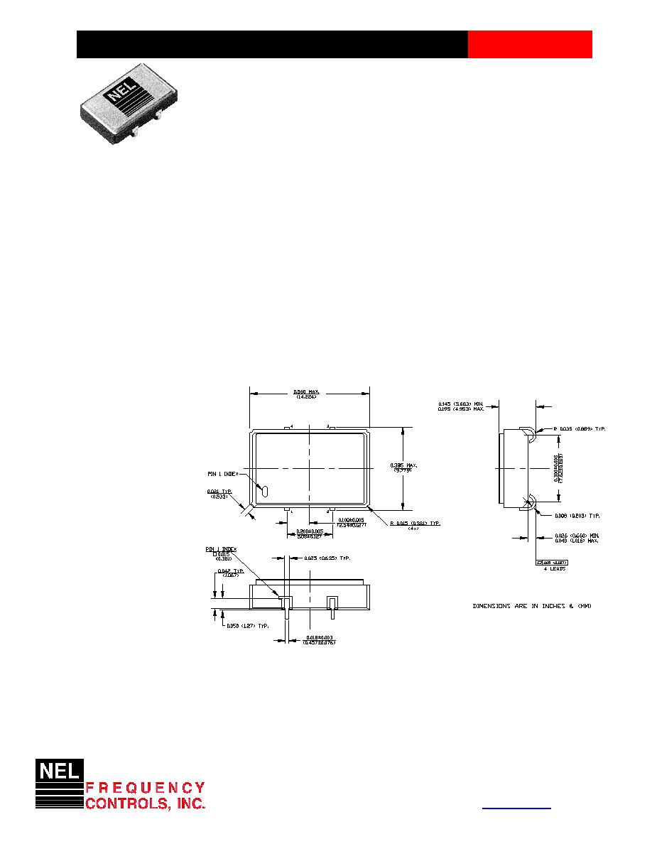
Electrical Connection
Pin Connection
1 Enable Input
2 Grd & Case
3 Output
4 V
DD
CRYSTAL CLOCK OSCILLATORS
Data Sheet 0010F
Rev. G
357 Beloit Street, P.O. Box 457, Burlington, WI 53105-0457 U.S.A. Phone 262/763-3591 FAX 262/763-2881
Email:
nelsales@nelfc.com
www.nelfc.com
SJ-1420 Series Continued
CMOS
Operating Conditions and Output Characteristics
Electrical Characteristics
Parameter
Symbol
Conditions
Min
Typical
Max
Frequency
-----
-----
40.1MHz
-----
80.0MHz
Duty Cycle
-----
@ V
DD
/2
45/55% -----
55/45%
Logic 0
V
OL
@ 600µA
-----
-----
0.2V
Logic 1
V
OH
@ 600µA
V
DD
-0.2V
-----
-----
Rise & Fall Time
tr,tf
10-90%
----- -----
8 ns
Tpz
-----
-----
-----
-----
25 ns
Enable/Disable
Logic High Voltage
-----
-----
3.5V
-----
-----
Enable/Disable
Logic Low Voltage
-----
-----
-----
-----
1.5V
Jitter, RMS
(2)
-----
-----
-----
-----
5 psec
Frequency Stability
(1)
dF/F
Overall conditions including:
-100ppm
-----
+100ppm
voltage, calibration, temp.,
10 yr aging, shock, vibration
General Characteristics
Parameter
Symbol
Conditions
Min
Typical
Max
Supply Voltage
V
DD
-----
4.75V
5.0V
5.25V
Supply Current
I
CC
No Load
0.0 mA
-----
40mA
Output current
I
O
-----
0.0 mA
-----
±16.0 mA
Operating temperature
T
A
-----
0∞C
-----
70∞C
Storage temperature
T
S
-----
-55∞C
-----
125∞C
Power Dissipation
P
D
-----
-----
-----
210 mW
Lead temperature
T
L
Soldering, 10 sec.
-----
-----
300∞C
Load
----
-----
-----
-----
15pf
Start-up time
t
S
-----
-----
2 ms
10 ms
Environmental and Mechanical Characteristics
Mechanical Shock Per MIL-STD-202, Method 213, Condition E
Thermal Shock
Per MIL-STD-833, Method 1011, Condition A
Vibration
0.060" double amplitude 10 Hz to 55 Hz, 35g's 55Hz to 2000 Hz
Soldering Condition
300∞C for 10 seconds
Hermetic Seal
Leak rate less than 1 x 10
-8
atm.cc/sec of helium
Footnotes:
1) Standard frequency stability (±20,±25,±50ppm & others available)
2) Jitter performance is frequency dependent. Please contact factory for full characterization.
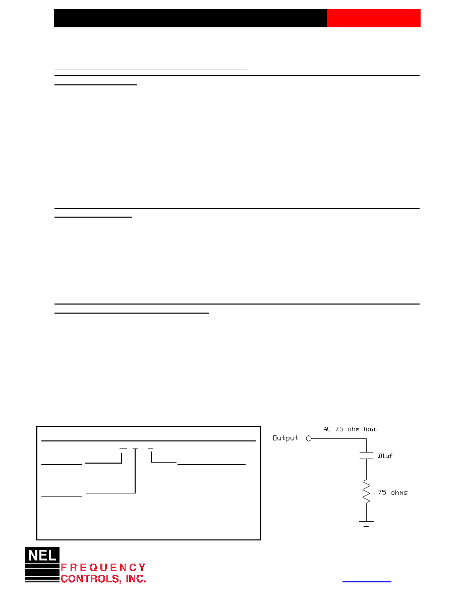
Test Load:
Rev. G
CRYSTAL CLOCK OSCILLATORS
SJ - A142X - FREQ
Package Code
Tolerance/Performance
SJ 4 J Lead SMD
0 ±100ppm 0-70∞C
1 ±50ppm 0-70∞C
7 ±25ppm 0-70∞C
Input Voltage
9 Customer Specific
Code Specification
A ±20ppm 0-70∞C
A 3.3V
B ±50ppm -40 to +85∞C
5V
C ±100ppm -40 to +85∞C
Creating a Part Number
Data Sheet 0010F