357 Beloit Street, P.O. Box 457, Burlington, WI 53105-0457 U.S.A.
Phone: 262-763-3591 Fax: 262-763-2881 Email: nelsales@nelfc.com www.nelfc.com
SU-A369X
Series
Size, mm
9 x 14
I/O
6 pad
Supply Voltage
3.3V
Features
∑ Frequency range≠300.0MHz to 1.5GHz
∑ Wide Absolute Pull Range
∑ Will withstand SMD reflow temperatures
of 253∞C for 4 minutes maximum
∑ Space-saving alternative to discrete
component oscillators
∑ High shock resistance, to 1000g
∑ 3.3 volt operation
∑ Low Jitter - Wavecrest jitter characterization
available
∑ High Reliability - NEL HALT/HASS
qualified for crystal oscillator start-up
conditions
∑ High Q Crystal actively tuned oscillator
circuit
∑ Power supply decoupling internal
∑ No internal PLL avoids cascading
PLL problems
∑ High frequencies due to proprietary design
∑ Gold plated pads
VCXO Series (PECL)
SU-A369X Series
Patent Pending Technology Rev E
Frequency Range: 300.0 MHz to 1.5 GHz
Creating a Part Number
SU - A369X - FREQ
Package Code
SU
6 pad 9x14mm SMD
Input Voltage
Code
Specification
A
3.3 V
APR/Performance
1 ±50 ppm 0-70∞C
9 Customer Specific
B ±50 ppm -40 to +85∞C
Drawing Specifications
Description
The SU-A369X Series
of voltage controlled quartz crystal oscillators provide frequency
control by applying a voltage to Pin 1. This unit supplies DPECL compatible outputs which are
enabled when Pin 2 is set to a logic low or left open.
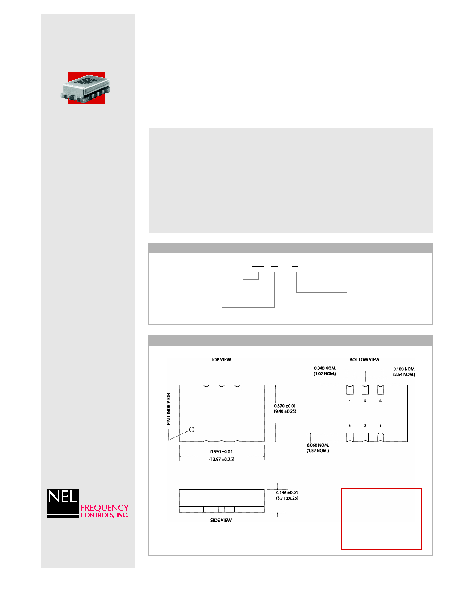
Electrical Connections
Pad
Connection
1
V
CO
2
Enable
3
V
EE
4
Output
5
Output Complement
6
V
CC
For the most up to date
specifications on each NEL
product, log on to our
website--www.nelfc.com
Dimensions shown in inches and (mm).

Operating Conditions and Output Characteristics
Electrical Characteristics
Parameter
Symbol
Conditions
Min
Typical
Max
Frequency
--
--
300.0 MHz
--
1.5 GHz
Duty Cycle
--
@V
O
/2
45/55%
--
55/45%
Logic 0
V
OL
--
V
CC
-1.810 Vdc
--
V
CC
-1.620 Vdc
Logic 1
V
OH
--
V
CC
-1.200 Vdc
--
V
CC
-0.880 Vdc
Rise & Fall Time
tr, tf
20-80% V
O
--
--
600 ps
Jitter, RMS
(1)
--
--
--
3 psec
--
Absolute Pull Range
(3)
APR
V
CO
= 0.3 to 3.0V
--
±100ppm
--
V
CO
Input Impedance
--
50na dc current max
100K ohm
--
--
V
CO
Linearity
--
V
CO
= 0.3 to 3.0V
--
--
10%
Transfer Function
(2)
--
V
CO
= 0.3 to 3.0V
--
Positive
--
Modulation Bandwidth
MBW
@-3dB, 0< V
CO
<3.3V
25kHz
--
--
Enable Voltage
(4)
--
with V
EE
=0V
0V
--
0.8V
Disable Voltage
--
with V
EE
=0V
2.0V
--
V
CC
General Characteristics
Parameter
Symbol
Conditions
Min
Typical
Max
Supply Voltage
V
CC
-V
EE
3.3V ±5%
3.135 V
3.3 V
3.465 V
Supply Current
I
CC
--
--
--
150 mA
Output Current
I
O
--
0.0 mA
--
±50.0 mA
Operating Temperature
T
A
--
0∫C
--
70∫C
Storage Temperature
T
S
--
-55∫C
--
125∫C
Power Dissipation
P
D
--
--
--
520 mW
Lead Temperature
T
L
Soldering, 10 sec.
--
--
300∫C
Load 50 ohm to V
CC
-2V or Thevenin Equivalent, Bias Required
Environmental and Mechanical Characteristics
Mechanical Shock
Per MIL-STD-202, Method 213, Condition E
Thermal Shock
Per MIL-STD-833, Method 1011, Condition A
Vibration
0.060" double amplitude 10 Hz to 55 Hz, 35g's 55 Hz to 2000 Hz
Soldering Condition
300∫C for 10 seconds
Hermetic Seal
Leak rate less than 1 x 10
-8
atm.cc/sec of helium
Footnotes:
1) Jitter performance is frequency dependent. Please contact factory for full Wavecrest characterization.
RMS jitter bandwidth of 12kHz to 20MHz.
2) Frequency increase with increase in control voltage and is monotonic.
3) Pullability is frequency dependant. Consult factory.
4) Open to enable pin also to enable the output.
VCXO Series (PECL)
SU-A369X Series
Patent Pending Technology Rev E
Frequency Range: 300.0 MHz to 1.5 GHz