
Revision 3.0
Subject to change without notice
1
NL82721R
Ternary Synchronous Content Addressable Memory
1Kx128
(128K)
IPCAM-1R
Description
The NL82721R is a 128K bit Ternary Synchronous Content Addressable Memory (IPCAM
TM
-1R). The NL82721R device
performs high-speed parallel search operations on memory tables. Its primary application is as an address filter or an address
translator for Fast Ethernet, Gigabit Ethernet, and ATM switches.
NL82721R has a mask word associated with every memory word. This enables the user to effectively store a "don't care" state
for compare operations (in addition to `0' and `1') making it a Ternary CAM. The Ternary nature of this CAM is ideal for
enabling policy enforcement and packet classification for differentiated services in edge, campus and enterprise networking
applications. The NL82721R has a streamlined instruction set and is a cost reduced version of the full-featured NL82721 device.
Features
� 1K x 128 Synchronous Ternary CAM Architecture
� 1K x 128 Local Mask Words allow masking of each
CAM word on a bit by bit basis.
� Match Flag times: 18/22 ns
� CAM Index output (pipelined mode): 10/12 ns
� Depth-expansion with no glue logic required
� Sustained 64-bit searches of up to 40 Million/Second
or 128-bit searches of up to 20 Million/second
� Separate 64-bit Comparand I/O bus, 64-bit Results bus
and 14-bit Instruction bus
� Two 128-bit wide Mask Registers for easy masking of
compare or write operations
� Single cycle execution of all instructions
� 3.3V TTL CMOS; 292-pin PBGA Package
Co
n
t
r
o
l
Lo
g
i
c
Address
Counter
Instruction Bus
Cascade In (Up & Down)
Reset
Chip Enable
M atch Flag In (Up & Dow n)
2
System M atch Flag
1K
x 12
8
C
A
M
A
r
r
a
y
Global M ask Registers 0 & 1
Status Register
RBUS
Comparand Bus
CBUS
64
MU
X
M ultiple M atch Flag
Full Flag Input
M atch Flag Out (Up & Down)
1
K
x
1
V
a
lid
it
y
B
i
t
0
127
Comparand Register
Results Bus
Clock
2
M ultiple M atch Flag Input
14
Cascade Out (Up & Down)
Full Flag
2
2
4
W ord Enables
64
32
32
Figure 1 NL82721R Block Diagram
128
Upper/Lower 64-bit Enable
CAM Word 0
Local M ask Word 0
Local M ask Word 1023
CAM Word 1023
128
1K
x 12
8 M
a
s
k
A
r
r
a
y
Revision 3.0
Subject to change without notice
2
NL82721R
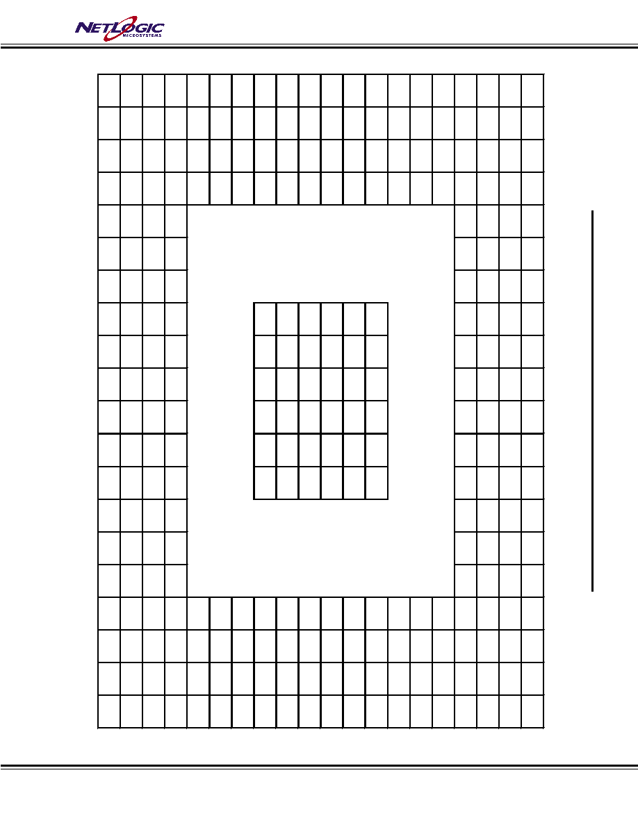
A
B
C
D
E
F
G
H
J
K
L
M
N
P
R
T
U
V
W
Y
20
CBUS50
CBUS51
CBUS54
CBUS56
CBUS59
CBUS61
CBUS62
(NC)
(NC)
(NC)
(NC)
(NC)
(NC)
RBUS30
RBUS29
RBUS27
RBUS24
RBUS22
RBUS19
RBUS18
20
19
CBUS49
CBUS48
CBUS53
CBUS55
CBUS57
CBUS60
CBUS63
(NC)
(NC)
(NC)
(NC)
(NC)
(NC)
(NC)
RBUS28
RBUS25
RBUS23
RBUS21
RBUS16
RBUS17
19
18
CBUS47
CBUS46
CBUS52
GND
CBUS58
VDD
(NC)
(NC)
(NC)
VDD
(NC)
(NC)
(NC)
VDD
RBUS31
RBUS26
GND
RBUS20
RBUS14
RBUS15
18
17
CBUS43
CBUS44
GND
GND
GND
VDD
VDD
GND
GND
VDD
VDD
GND
GND
VDD
VDD
GND
GND
GND
RBUS12
RBUS11
17
16
CBUS42
CBUS41
CBUS45
GND
GND
RBUS13
RBUS09
RBUS10
16
15
CBUS37
CBUS38
CBUS40
VDD
VDD
RBUS08
RBUS06
RBUS05
15
14
CBUS35
CBUS36
VDD
VDD
VDD
VDD
RBUS04
RBUS03
14
13
CBUS32
CBUS34
CBUS39
GND
GND
GND
GND
GND
GND
GND
GND
RBUS07
RBUS02
RBUS00
13
12
CBUS30
CBUS31
CBUS33
GND
GND
GND
GND
GND
GND
GND
GND
RBUS01
(NC)
(NC)
12
11
CBUS27
CBUS28
CBUS29
VDD
GND
GND
GND
GND
GND
GND
VDD
(NC)
(NC)
(NC)
11
10
CBUS25
CBUS26
VDD
VDD
GND
GND
GND
GND
GND
GND
VDD
VDD
(NC)
(NC)
10
9
CBUS24
CBUS22
CBUS23
GND
GND
GND
GND
GND
GND
GND
GND
(NC)
(NC)
(NC)
9
8
CBUS21
CBUS20
CBUS19
GND
GND
GND
GND
GND
GND
GND
GND
(NC)
(NC)
(NC)
8
7
CBUS18
CBUS17
CBUS16
VDD
VDD
(NC)
(NC)
(NC)
7
6
CBUS15
CBUS14
VDD
VDD
VDD
VDD
(NC)
(NC)
6
5
CBUS12
CBUS11
CBUS13
GND
GND
(NC)
(NC)
(NC)
5
4
CBUS10
CBUS08
CBUS09
GND
GND
VDD
VDD
GND
GND
VDD
VDD
GND
GND
VDD
VDD
GND
GND
(NC)
(NC)
(NC)
4
3
CBUS06
CBUS07
GND
/RST
IBUS01
IBUS05
VDD
IBUS10
IBUS13
/WEN3
VDD
VDD
CSCDI
(NC)
VDD
GND
GND
GND
(NC)
(NC)
3
2
CBUS04
CBUS05
CBUS03
IBUS00
IBUS03
IBUS06
IBUS08
IBUS11
CLK
/WEN2
/WEN0
/MMFI
/MFDI
CSCUO
/MFDO
/SMF
/FF
(NC)
(NC)
(NC)
2
1
CBUS02
CBUS01
CBUS00
IBUS02
IBUS04
IBUS07
IBUS09
IBUS12
/CE
ULEN
/WEN1
/FFI
CSCUI
(NC)
CSCDO
(NC)
/MMF
(NC)
(NC)
(NC)
1
A
B
C
D
E
F
G
H
J
K
L
M
N
P
R
T
U
V
W
Y
Figure 2 NL82721 Ball Assignment (292 PBGA, Top View)
Revision 3.0
Subject to change without notice
3
NL82721R
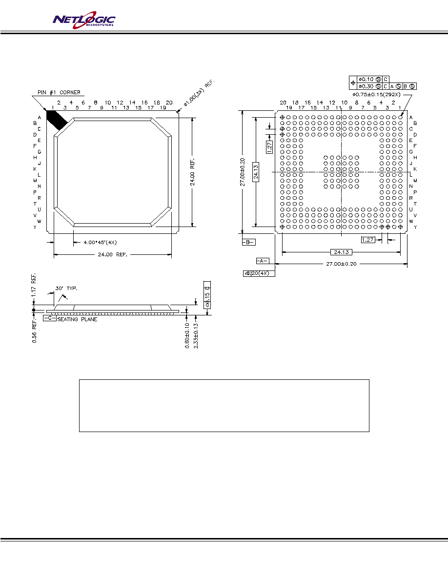
Figure 3: 292 PBGA Package Dimensions

Revision 3.0
Subject to change without notice
4
NL82721R
1.0 Functional Description
The NL82721R is a Synchronous Content Addressable
Memory (IPCAM-1R) designed for use as an address filter
or an address translator in 100/1000 Mb/s Ethernet switches
and routers. This device can also be used to implement fast
routing tables in Internet Protocol (IP) switches. The
NL82721R has a total associative memory capacity of
128K bits organized as 1K x 128 bits.
Each 128-bit memory word has associated with it a 128-bit
local mask word that is used during compare operation. In
contrast to global masks, these local mask words are used
only with their associated word. This local mask is used
only for compare instructions and is always used (not
deselectable as global masks). This provides masking on
an individual bit basis and hence Ternary CAM capability.
This masking on a per bit basis capability is useful to store
subnet masks in Internet Protocol (IP). The NL82721R is a
member of NetLogic's IPCAM-1R family.
A bi-directional 64-bit Comparand Bus (CBUS) enables all
internal registers and memory to be accessed. An output
only, 32-bit Results Bus (RBUS) provides status
information after a compare operation. A 14-bit Instruction
Bus (IBUS) allows instructions to be presented to the
device once every cycle. All operations on the device are
timed synchronously with the rising edge of a free running
clock.
The Comparand Register (CR) is a 128-bit register that
enables the user to write the comparand data (key) and
compare it with the contents of memory. This is the only
register that enables a user to store and compare data with
memory.
The NL82721R has two Global Mask Registers (GMR1-
GMR0) that can each be selected on an operation by
operation basis for write or compare operations. For a write
operation, when the bits in these registers are programmed
with `1's, the corresponding bits in memory will be
masked, i.e. will not be written into. For compare
operations using Global Mask Registers, the corresponding
bits in the associative data word will be forced to a match.
The 16-bit Device Configuration Register (DCR) enables
the user to configure the device operation. The RBUS of
the IPCAM-1R operates in Pipeline Mode only. The
Address Counter may be set to be incremented
automatically during write and so on. See Table 3f for a
complete list.
The Status Register (SR) holds status information after
compare, read, write or copy operations.
A 10-bit Address Counter (ACR) supplies the address to
the memory array. This counter may be loaded with any
valid start address and can be configured to increment once
every cycle for read or write operations. This allows data
to be loaded into or read out of the memory continuously.
An Upper 64-bit/Lower 64-bit enable pin (ULEN) allows
access to either the upper 64-bits or the lower 64-bits of the
128-bit words of memory and registers.
Four Word Enable (/WEN3-/WEN0) inputs allow access to
the internal registers and memory on 16-bit boundaries.
These inputs also allow
for bus matching on the CBUS
with no glue logic.
The NL82721R can be clocked up to frequencies of
40MHz with a free running clock. A Chip Enable (/CE)
input allows the device to be selected or deselected similar
to any memory device. The device has flag inputs and
outputs that enable depth cascading with no glue logic.
2.0 Pin Description
2.1 Clock (CLK)
This is a free running clock that is used to time all
transactions on the CAM. The rising edge of the clock is
the timing reference.
2.2 Chip Enable (/CE)
This is a synchronous input that selects the device for all
operations, when asserted low. When asserted high, the
device is deselected and is in idle mode. In idle mode, the
CBUS and the RBUS are High-Z. For single device
operation, when the device is deselected (/CE asserted
high) the Match, Multiple Match and System Match Flags
are high and Full Flag is low. For depth cascaded devices,
the deselected devices will pass the flag input states
through to the flag outputs. See Table 1.
2.3 Reset (/RST)
This is an asynchronous input and provides the hardware
reset for the device. During initialization, this pin must be
asserted low for a minimum of three (3) cycles. This will
set all CAM words to empty, initialize the control logic,
and clear all registers. The reset operation must be followed
by at least one NOP instruction. Tables 2 and 3a-3d
illustrate the state of the part after reset.
2.4 Full Flag Input (/FFI)
This input is provided for depth cascading multiple CAMs.
When asserted low, this pin will allow data to be written
into the CAM at the next free address (NFA) using the
"Write to memory at NFA" instruction provided the device
is not full. However, write to memory at address specified
by the Address Counter is not affected by full flag input or
output. For single device operation, the /FFI pin is tied to
ground. For depth cascaded devices, the highest priority
device has its /FFI input tied to ground, all other devices in
the cascade having the /FFI tied to the Full Flag output
(/FF) of the next higher priority device. Refer to the depth
cascading section for more details.
2.5 Match Flag Up Input (/MFUI)
This input is provided for depth cascading multiple CAMs.
For single device operation, this pin is tied to VDD. For
depth cascaded devices, the lowest priority device has its
/MFUI pin connected to VDD. All other devices in the
cascade have their /MFUI pin tied to the Match Flag Up
Output (/MFUO) of the next Lower priority device. Refer
to the depth cascading section for more details.

Revision 3.0
Subject to change without notice
5
NL82721R
2.6 Match Flag Down Input (/MFDI)
This input is provided for depth cascading multiple CAMs.
For single device operation, this pin is tied to VDD. For
depth cascaded devices, the highest Priority device has its
/MFDI pin connected to VDD. All other devices in the
cascade have their /MFDI pin tied to the Match Flag Down
Output (/MFDO) of the next higher priority device. Refer
to the depth cascading section for more details.
2.7 Multiple Match Flag Input (/MMFI)
This input is provided for depth cascading multiple CAMs.
For single device operation, this pin is tied to VDD. For
depth cascaded devices the highest priority device has its
/MMFI tied to VDD. All other devices in the cascade have
their /MMFI pin tied to the Multiple Match Flag (/MMF) of
the next higher Priority device. Refer to the depth
cascading section for more details.
2.8 Cascade Down Input (CSCDI)
This input is provided for depth cascading multiple CAMs.
For single device operation, this pin is tied to ground. For
depth cascaded devices the highest priority device has its
CSCDI connected to ground. All other devices in the
cascade have their CSCDI pin tied to the CSCDO of the
next higher priority device. Refer to the depth cascading
section for more details.
2.9 Cascade Up Input (CSCUI)
This input is provided for depth cascading multiple CAMs.
For single device operation, this pin is tied to ground. For
depth cascaded devices the lowest Priority device has its
CSCUI connected to ground. All other devices in the
cascade have their CSCUI pin tied to the CSCUO of the
next lower priority device. Refer to the depth expansion
section for more details.
2.10 Upper/Lower 64-bit Enable (ULEN)
This is a synchronous input and enables access to the upper
64-bits or the lower 64-bits of the 128-bit memory,
Memory Configuration, Global Mask, Comparand, Data
Translation and Status Registers. When ULEN is high, it
enables access to the upper 64 bits of the 128 bits; when it
is low, it enables access to the lower 64 bits of the 128 bits.
2.11 Word Enable (/WEN_0,1,2,3)
This is a synchronous input and enables access to the CAM
array and all the registers with 16-bit granularity. For 64-
bit entities in the CAM, /WEN_3 enables access to bits 63-
48, /WEN_2 to bits 47-32, /WEN_1 to bits 31-16 and
/WEN_0 to bits 15-0. These control pins are effective only
for read and write to memory and the registers; for all other
operations they are a "don't care".
2.12 Instruction Bus (IBUS
13
- IBUS
0
)
This is a synchronous 14-bit bus that provides the operation
code (Opcode) to the CAM.
2.13 Comparand Bus (CBUS
63
- CBUS
0
)
This is a 64-bit synchronous I/O bus that conveys data to
and from the memory and the registers.
2.14 Cascade Down Output (CSCDO)
This output is provided for depth cascading multiple
CAMs. For single device operation this pin must be left
unconnected. For depth cascaded devices, the highest
priority device has its CSCDO connected to the CSCDI of
the next lower priority device. Refer to the depth
expansion section for more details.
2.15 Cascade Up Output (CSCUO)
This output is provided for depth cascading multiple
CAMs. For single device operation this pin must be left
unconnected. For depth cascaded devices, the lowest
priority device has its CSCUO connected to the CSCUI of
the next higher priority device. Refer to the depth
expansion section for more details.
2.16 Full Flag (/FF)
This is a synchronous output and is updated after Write to
Memory, Copy to Memory, set VBIT, or Set Full Flag
operations. After reset, this pin is high. When the device is
full, /FF is asserted low. For depth cascaded devices, /FF is
connected to /FFI of the next lower priority device. For
depth cascaded devices, when single device mode is
selected, deselected devices pass /FFI through to /FF.
2.17 Match Flag Up Output (/MFUO)
This synchronous output is provided for depth cascading
CAMs. This output is updated for all compare operations.
After reset, /MFUO is high. For depth cascaded devices,
the /MFUO of a device is connected to the /MFUI of the
next higher priority device. For depth cascaded devices,
when single device mode is selected, deselected devices
pass /MFUI through to /MFUO.
2.18 Match Flag Down Output (/MFDO)
This synchronous output is provided for depth cascading
CAMs. This output is updated for all compare operations.
After reset, /MFDO is high. For depth cascaded devices,
the /MFDO of a device is connected to the /MFDI of the
next lower priority device. For depth cascaded devices,
when single device mode is selected, deselected devices
pass /MFDI through to /MFDO.
2.19 System Match Flag (/SMF)
This synchronous output provides the System Match Flag
(either for single device or cascaded devices). This output
is updated for all compare operations. After reset /SMF is
high. Functionally this output is identical to /MFDO.
When cascading, the /SMF is provided by the lowest
priority CAM. The /SMF from all other CAMs in the
cascade may be left unconnected.
2.20 Multiple Match Flag (/MMF)
This synchronous output provides the Multiple Match Flag
(either for single device or cascaded devices). This output
is updated for all compare operations. After reset /MMF is
high. In depth cascaded systems the lowest priority device
provides the /MMF. For cascaded devices, when single
device mode is selected, the deselected devices pass
/MMFI through to /MMF.