 | –≠–ª–µ–∫—Ç—Ä–æ–Ω–Ω—ã–π –∫–æ–º–ø–æ–Ω–µ–Ω—Ç: NHI-1523 | –°–∫–∞—á–∞—Ç—å:  PDF PDF  ZIP ZIP |
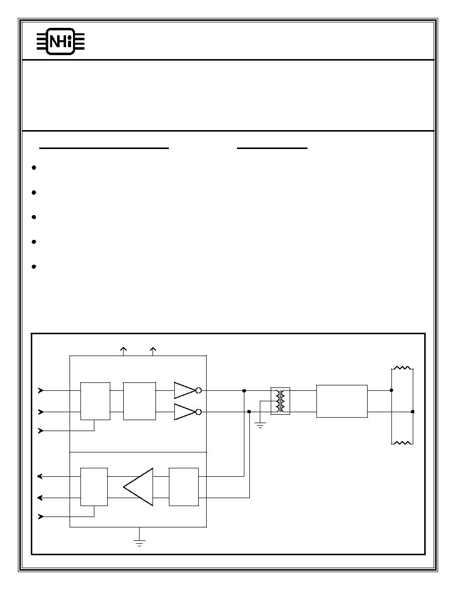
Isolation
Transformer
Direct
Or
Transformer
Coupler Box
Data Bus
TXOUT
TXOUT_L
RXIN
RXIN_L
RX
Input
Filter
Comparator
RX
Receive
Logic
RECEIVER
RXENA
RX_L
RX
TXINH
TX_L
TX
TRANSMITTER
TX
Transmit
Logic
Shaping
Network
Figure I: Block Diagram
(Each Channel)
+5V
+12V
Features/Applications:
Description:
Very Low Standby Power
Low Thermal Resistance
Totally Isolated Channels
Short Circuit Proof
Superior Noise Performance
The NHI +12V dual transceivers are available in
1.900" x .780", 36 pin plug-in and flatpack packages.
Each receiver converts the 1553 bus bi-phase data to
complementary RX and RX_L TTL digital outputs
for use by the manchester decoder. The device
provides independent receiver enables for each
channel. Devices are available with receiver outputs
normally HIGH or LOW during standby mode for
compatibility with industry standard decoders.
The transmitters will output bi-phase manchester to
the coupling transformer when the TX and TX_L
inputs are driven by complementary TTL digital data.
The device provides an independent transmitter
inhibit TXINH for each channel.
Mil-Std-1553 Products
NHI-1523 Series
+12V Dual Transceivers
NATIONAL HYBRID, INC.
2200 Smithtown Avenue, Ronkonkoma, NY 11779
(516) 981-2400 FAX 516-981-8888
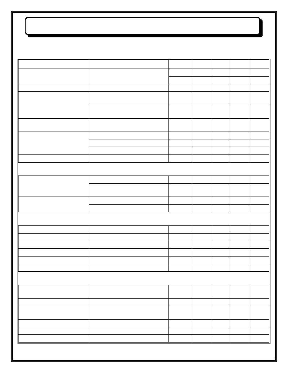
Parameter
Condition
Symbol
Min
Typ
Max
Units
POWER SUPPLY
Vcc
4.5
5.5
V
REQUIREMENTS
+V
11.4
12.6
V
V
CC
SUPPLY CURRENT
Vcc=5.0V, +V=12.0V, total hybrid
Icc
25
mA
+V SUPPLY CURRENT
Vcc=5.0V, +V=12.0V, each channel,
not transmitting
+I
25
mA
Vcc=5.0V, +V=12.0V, One channel
@ 100% duty cycle
+I
100%
210
mA
POWER DISSIPATION
Vcc=5.0V, +V=12.0V, Transmit one
channel @ 100% duty cycle
Pd2
0.96
W
OPERATING
Junction
Tj
-55
160
∞C
TEMPERATURES
Case
Tc
-55
125
∞C
Storage
Ts
-65
150
∞C
THERMAL IMPEDANCE
Junction to Case
jc
8.8
∞C/W
LOGIC I/O
RXENA_A, TXA, TXA_L,
Vcc= 5.5V, Vil= 0.0V
Iil
-0.8
mA
TXINH_A, RXENA_B, TXB,
TXB_L, TXINH_B
Vcc= 4.5V, Vih= 2.7V
Iih
40
uA
RXA, RXA_L, RXB, RXB_L
Vcc= 5.5V, Iol= -8 mA
Vol
0.5
V
Vcc= 4.5V, Ioh= 400 uA
Voh
2.5
V
RECEIVER
Input Resistance
1 MHz sine wave
Rin
7
k
Input Capacitance
1 MHz sine wave
Cin
5
pF
Common Mode Rejection Ratio
CMRR
40
dB
Threshold Voltage
Differential
Vth
0.56
1.0
Vpp
Input Level
Differential
Vin
40
Vpp
Receiver Delay
Zero Crossing on bus to RX or RX_L
t
RD
400
nS
TRANSMITTER
Output Voltage
Across 35 W load
TXVOC = +V = 12.0V
V
OUT
6
9
Vpp
Rise/Fall Time
10% to 90% of peak to peak output
t
R
, t
F
100
150
300
nS
Transmitter Delay
TX or TX_L edge to bus zero
crossing
t
TD
250
nS
Output Dynamic Offset Voltage
Across 35 W load
Vdyn
-90
90
mV
Output Noise
Differential
Vnpp
10
mVpp
Output Resistance
Differential, not transmitting
Rout
10
k
NHI-1523
TABLE I: Electrical Specifications
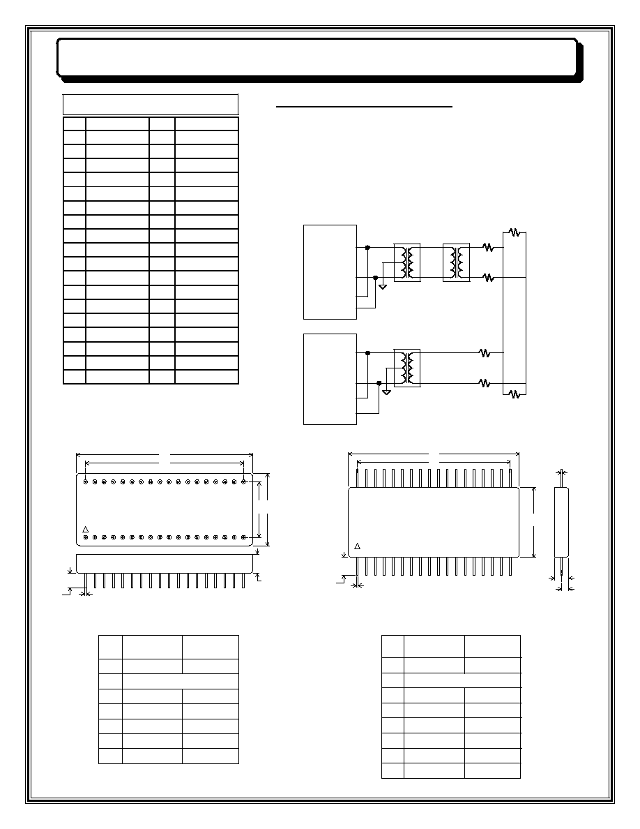
A
B
D
C
E
G
F
36
19
18
1
H
TOP VIEW
36 Pin Flatpack Package Detail
DIM
TYP
TOL
(inches)
(+/- inches)
A
B
C
D
E
F
G
1.900 SQ
0.010
17 EQ SP @ 0.100 = 1.700
0.780
0.010
0.185
0.012
0.080
0.010
0.500
MIN
0.018
0.002
H
0.010
0.002
A
B
D C
E
G
F
36
19
18
1
TOP VIEW
36 Pin Plug-In Package Detail
DIM
TYP
TOL
(inches)
(+/- inches)
A
B
C
D
E
F
G
1.900 SQ
0.010
17 EQ SP @ 0.100 = 1.700
0.780
0.010
0.600
0.010
0.185
0.010
0.250
MIN
0.018
0.002
NHI-1523
36 Pin Package Functions
Pin#
Function
Pin#
Function
1
TXOUT_A
36
TXA_L
2
TXOUT_A_L
35
TXA
3
GND_A
34
TXINH_A
4
NC
33
+5V_A
5
RXA
32
NC
6
RXENA_A
31
NC
7
GND_A
30
RXIN_A_L
8
RXA_L
29
RXIN_A
9
NC
28
+12V_A
10 TXOUT_B
27
TXB_L
11 TXOUT_B_L
26
TXB
12 GND_B
25
TXINH_B
13 NC
24
+5V_B
14 RXB
23
NC
15 RXENA_B
22
NC
16 GND_B
21
RXIN_B_L
17 RXB_L
20
RXIN_B
18 NC
19
+12V_B
TRANSFORMER COUPLED
NHI-1523
TXOUT
TXOUT_L
RXIN
RXIN_L
1.25:1
NHI-1523
TXOUT
TXOUT_L
RXIN
RXIN_L
DIRECT COUPLED
55
55
Zo
Zo
.75Zo
.75Zo
1.66:1 1:1.4
Figure II: BUS Connections
Transformer Requirements:
The NHI-1523 requires a transformer with a turns ratio of
1.25:1.00 for Direct Coupling, and a turns ratio of
1.66:1.00 for Transformer Coupling to the Mil-Std-1553
Bus. Technitrol part number Q1553-3 or equivalent is
recommended. The center tap on the transceiver side of
the isolation transformer must be grounded.

Ordering Information:
NHI-1523 FP / M
Reliability Grade
M
= Military, -55 to +125 ∞C
Blank = Industrial, -40 to +85 ∞C
Package Style
FP
= Flatpack
Blank = Plug-In
Decoder Compatibility
22
= RX & RX_L, Standby = Logic 1
23
= RX & RX_L, Standby = Logic 0
** SMD Listing: DESC Drawing# 5962-89826
See QML-38534 for NHI's Manufacturer Qualification Under Mil-PRF-38534
Fully Compliant with Mil-Std-883
883
=
Transmitter Operation:
A high level input on TXINH will
inhibit the transmitter outputs. If the
TX & TX_L transmitter inputs are
both high or both low, the
transmitter is also inhibited.
Receiver Operation:
A low level input on RXENA will
disable the receiver outputs RX &
RX_L regardless of bus activity.
The receiver output compatibility
may be specified as logic 0 or logic 1
when in standby mode.
** See Ordering Information
TX_L
TX
Vout
(Line to Line)
RX_L
RX
Vin
(Line to Line)
Transmit Waveforms
Receive Waveforms
t
TD
t
RD
NHI-1523