 | –≠–ª–µ–∫—Ç—Ä–æ–Ω–Ω—ã–π –∫–æ–º–ø–æ–Ω–µ–Ω—Ç: NHI6433 | –°–∫–∞—á–∞—Ç—å:  PDF PDF  ZIP ZIP |

NATIONAL HYBRID INC.
RONKONKOMA N.Y. 11779
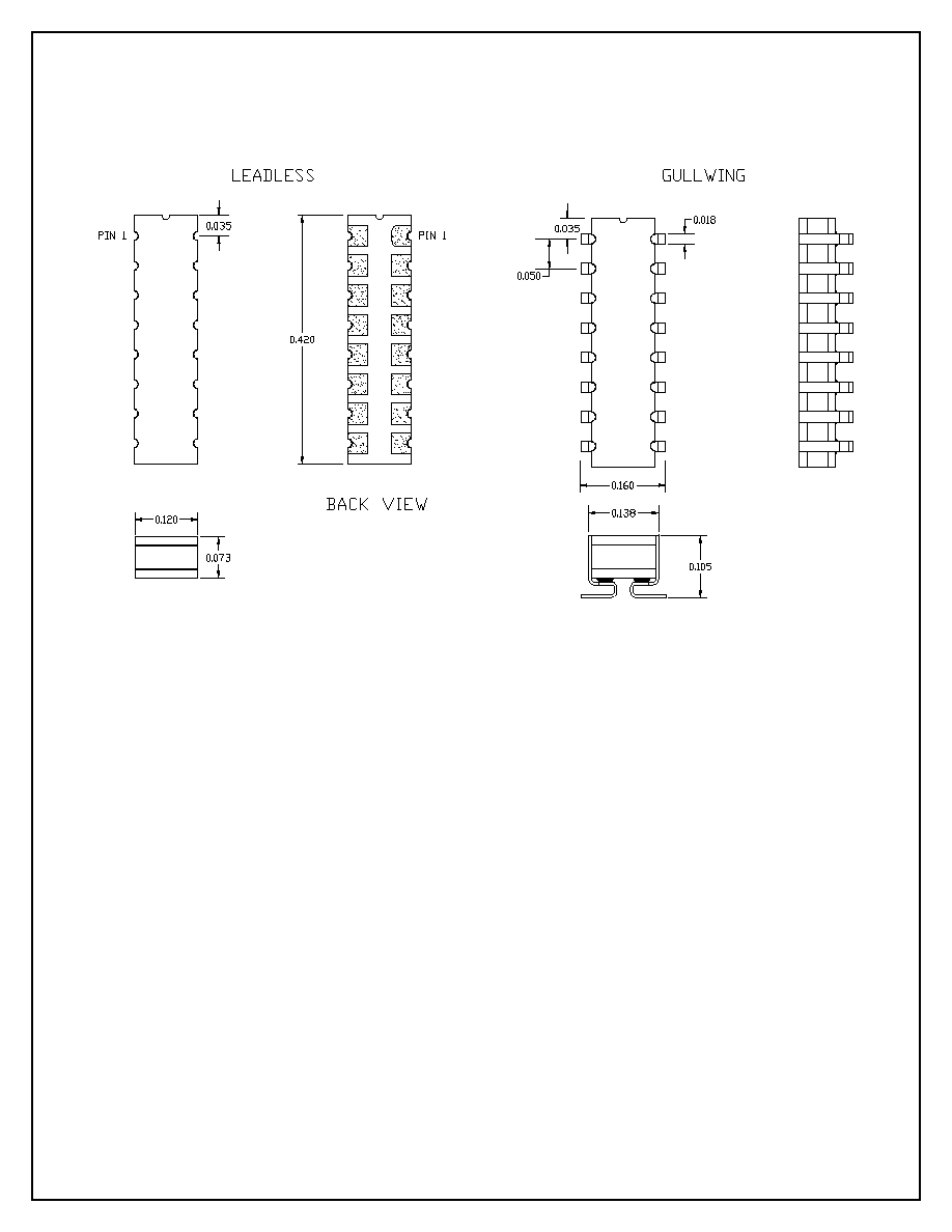
Hermetically Sealed, 4-Channel,
Darlington Optocoupler NHI 6433
Features;
∑ -55∞c to +125∞c Operation
∑ High CTR typ >200% @ If=1.0mA
∑ Output Voltage to 30V
∑ Withstanding Voltage > 1500Vdc
∑ High Radiation Tolerance
∑ Functionally Compatible with four 4N33
Absolute Maximum Ratings;
Supply Voltage (Vcc) ......................................... -0.5 to 30Vdc
Continuous Current If ......................................... 60mA
Reverse Input Voltage Vr .................................... 5 Vdc
Output Current .................................................. 100mA
Output Voltage ..................................................-0.5 to 30Vdc
Storage Temperature ......................................... -65∞C to 150∞C
Lead Solder Temperature ................................... 260∞C for 10 sec.
Junction Temperature .........................................175∞C
Recommended Operating Conditions;
Output Voltage Range .................................................... to 30Vdc
Input Current ................................................................... 0.5 mA to 15mA
Ambient Operating Temperature Range ........................ -55∞C to 125∞C
2
1
3
4
7
6
5
8
1 5
1 6
1 4
1 3
1 0
1 1
1 2
9
Terminal
Number
Terminal-
Function
1
Anode 1
2
Cathode 1
3
Anode 2
4
Cathode 2
5
Anode 3
6
Cathode 3
7
Anode 4
8
Cathode 4
9
Emitter 4
10
Collector 4
11
Emitter 3
12
Collector 3
13
Emitter 2
14
Collector 2
15
Emitter 1
16
Collector 1
Page1
NHI 6433
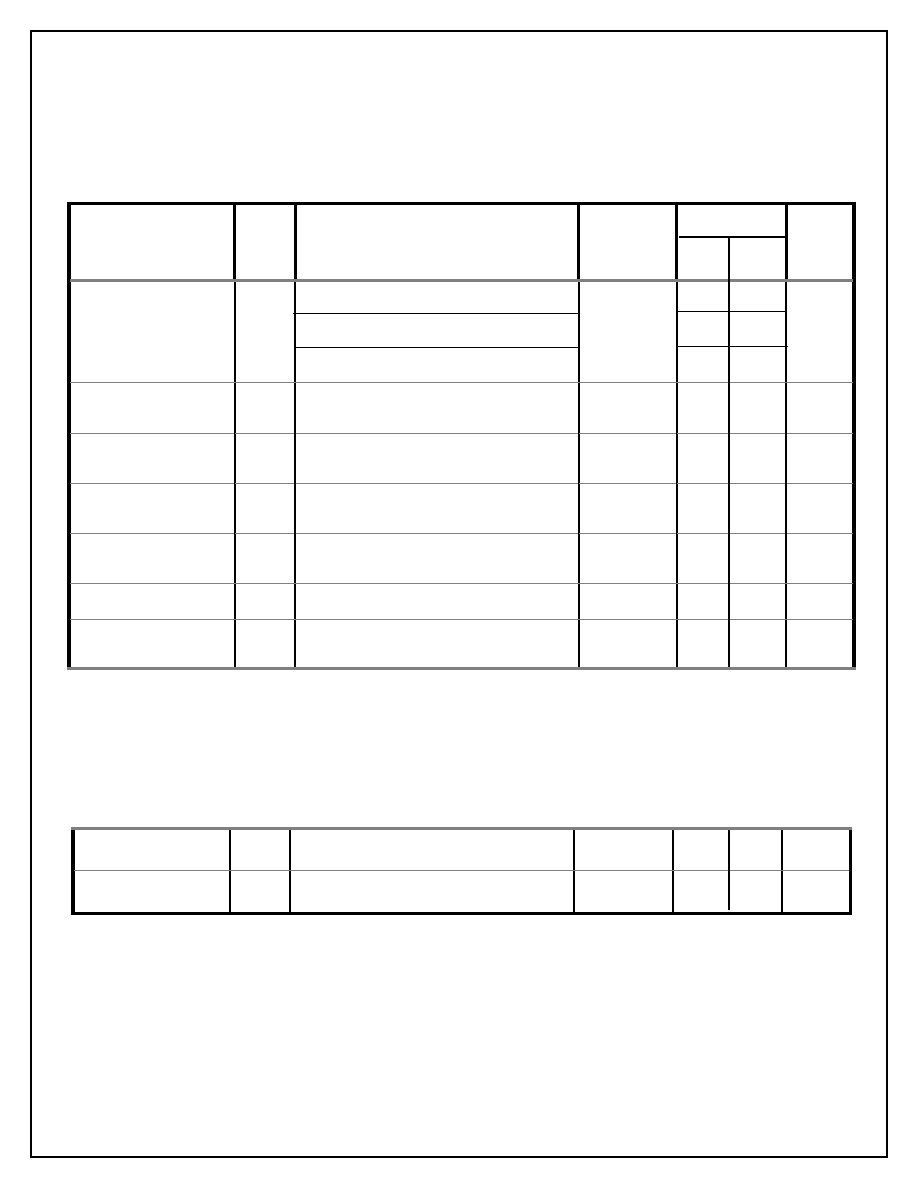
TEST
SYM-
BOL
TEST CONDITIONS
GROUP
A SUB-
GROUP
LIMITS
MIN MAX
UNITS
Current Transfer Ratio
Ctr
Vce = 10V, If =1mA (at Ta = 25∞C) _1
Vce = 10V, If =1mA (at Ta = -55∞C) _1
Vce = 10V, If =1mA (at Ta = 125∞C)_1
1,2,3
500
500
200
%
Collector-Emitter
Breakdown Voltage
Vceo Ic = 100uA
30 60
Vdc
Emitter ≠ Collector
Breakdown
Veco Ie = 100Ua
5.0 7.5
Vdc
Output Saturation
Voltage
Vce
(sat)
If= 8mA , Ic=2.0mA
1,2.3
1.0
Vdc
High Level Output
Current (dark current) Iceo Vcc = 10V, If = 0µA
1,2,3
100
nAdc
Input Forward Voltage Vf
If = 10mA
1,2
1.7
Vdc
Input Reverse Break-
down Voltage
Vbr
Ir = 10µA
1,2,3
5.0 30 Vdc
Turn on time
Ton If = 200mA, Ic = 50mA, Vcc = 10V
9,10,11
5.0
uS
Turn-off time
Toff
If = 200mA, Ic = 50mA, Vcc = 10V
9,10,11
100 uS
Page2
NHI 6433
Electrical Performance Characteristics:
(at Ta = 25∞C unless otherwise specified)
Switching Characteristics:
(at Ta = 25∞C unless otherwise specified

_1 Ctr is defined as the ratio of the Output Collector current (Io) to the LED Forward Current ( If ), times 100%.
_2 Device is considered a two terminal device. Pins 1 and 2 are shorted together and pins 4 and 5 are shorted
together.
_3 Measured between the LED cathode and pins 4 and 5 (shorted together).
_4 Parameters shall be tested as part of the device's initial characterization . Parameters are guaranteed to the limits
specified for all lots not specifically tested.
_5 Cmh is the maximum common mode transient to assure that the output will remain in a high logic state (Vo > 2.0V).
_6 Cml is the maximum common mode transient to assure that the output will remain in a low logic state (Vo < 0.8V).
_7 In applications where dV/dt may exceed 50,000 Vµs a series resistor must be included in the Vcc line to limit
destructively high surge currents. The recomended value, at If = 0.5mA, is 3.3K
TEST
SYM-
BOL
CONDITIONS
GROUP
A SUB-
GROUP
LIMITS
MIN
UNITS
Capacitance,
input to output
Cio
f = 1Mhz, Ta = 25∞C _ 3_4
4
4
pF
Common Mode
Transient Immunity,
high output
Cmh
Vcm = 25v (peak)
Vcc = 5.0v, Rl = 2.0K _4_5_7
If = 0mA,
9,10,11
500
V/µs
Common Mode
Transient Immunity,
lo output
Cml
Vcm = 25v (peak)
Vcc = 5.0v, Rl = 2.0K _4_6_7
If = 0mA,
9,10,11
500
V/µs
Isolation Voltage
Viso Ii-o 1uA _2_4
1500
Vdc
Notes;
Isolation Characteristics:
(at Ta = 25∞C unless otherwise specified)
Page3
NHI 6433
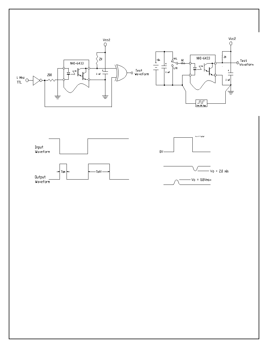
Fig 1 Switching Time Test Circuit
Fig 2 Common Mode Test circuit
Fig 3 Switching Time Test Waveform
Fig 4 Common Mode Test Waveform
Page4
NHI 6433
Page5
NHI 6433