DS25BR400
Quad Transceiver with Input Equalization and Output
De-Emphasis
General Description
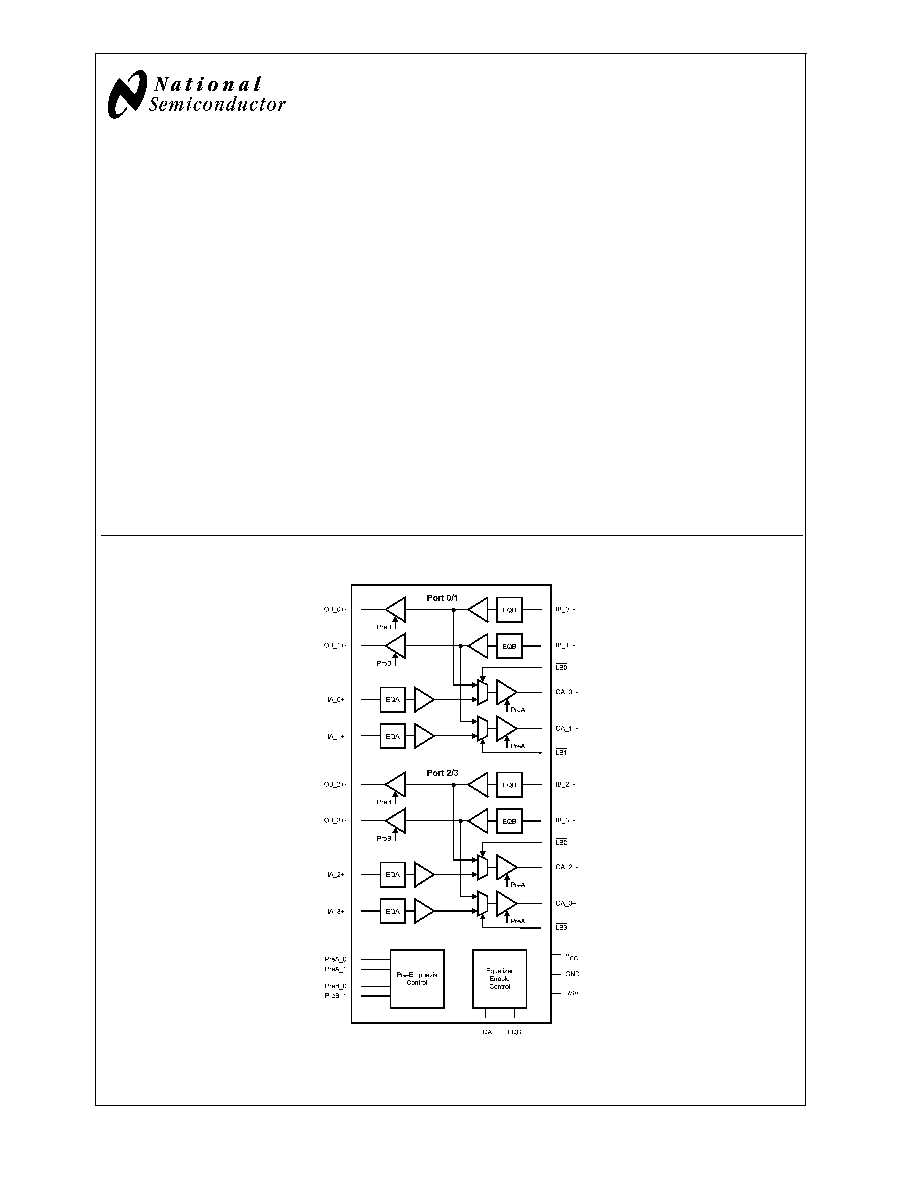
The DS25BR400 is a quad 250 Mbps ≠ 2.5 Gbps CML
transceiver, or 8-channel buffer, for use in PCI Express,
SATA, SAS, Fibre Channel backplane and cable applica-
tions. With operation down to 250 Mbps, the DS25BR400
can be used in applications requiring both low and high
frequency data rates. Each input stage has a fixed equalizer
to reduce ISI distortion from board traces. The equalizers are
grouped in fours and are enabled through two control pins.
These control pins provide customers flexibility in PCI Ex-
press applications where ISI distortion may vary from one
direction to another. All output drivers have four selectable
steps of de-emphasis to compensate against transmission
loss across long FR4 backplanes. The de-emphasis blocks
are also grouped in fours. In addition, the DS25BR400 also
has loopback control capability on four channels. All CML
drivers and receivers are internally terminated with 50
pull-up resistors.
Features
n
Quad 2.5 Gbps Transceiver or 8-Channel CML Serial
Buffer
n
250 Mbps ≠ 2.5 Gbps Fully Differential Data Paths
n
Optional Fixed Input Equalization
n
Selectable Output De-emphasis
n
Individual Loopback Controls
n
On-chip Termination
n
+3.3V supply
n
Low Power, 1.3 Watts MAX
n
Lead-less eLLP-60 pin package
(9mmx9mmx0.8mm, 0.5mm pitch)
n
-40∞C to +85∞C Industrial Temperature Range
n
6 kV ESD Rating, HBM
Functional Block Diagram
20194201
June 2006
DS25BR400
Quad
T
ransceiver
with
Input
Equalization
and
Output
De-Emphasis
© 2006 National Semiconductor Corporation
DS201942
www.national.com
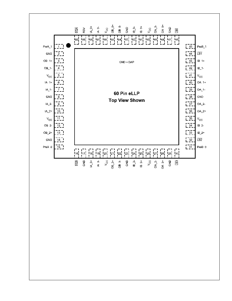
Connection Diagram
20194202
Leadless eLLP-60 Pin Package
(9mmx9mmx0.8mm, 0.4mm pitch)
Order number DS25BR400TSQ
See NS Package Number SQA060
DS25BR400
www.national.com
2

Pin Descriptions
Pin Name
Pin
Number
I/O
Description
DIFFERENTIAL I/O
IB_0+
IB_0-
51
52
I
Inverting and non-inverting differential inputs of port_0. IB_0+ and IB_0- are internally
connected to a reference voltage through a 50
resistor.
OA_0+
OA_0-
48
49
O
Inverting and non-inverting differential outputs of port_0. OA_0+ and OA_0- are connected
to V
CC
through a 50
resistor.
IB_1+
IB_1-
43
42
I
Inverting and non-inverting differential inputs of port_1. IB_1+ and IB_1- are internally
connected to a reference through a 50
resistor.
OA_1+
OA_1-
40
39
O
Inverting and non-inverting differential outputs of port_1. OA_1+ and OA_1- are connected
to V
CC
through a 50
resistor.
IB_2+
IB_2-
33
34
I
Inverting and non-inverting differential inputs of port_2. IB_2+ and IB_2- are internally
connected to a reference voltage through a 50
resistor.
OA_2+
OA_2-
36
37
O
Inverting and non-inverting differential outputs of port_2. OA_2+ and OA_2- are connected
to V
CC
through a 50
resistor.
IB_3+
IB_3-
25
24
I
Inverting and non-inverting differential inputs of port_3. IB_3+ and IB_3- are internally
connected to a reference voltage through a 50
resistor.
OA_3+
OA_3-
28
27
O
Inverting and non-inverting differential outputs of port_3. OA_3+ and OA_3- are connected
to V
CC
through a 50
resistor.
IA_0+
IA_0-
58
57
I
Inverting and non-inverting differential inputs of port_0. IA_0+ and IA_0- are internally
connected to a reference voltage through a 50
resistor.
OB_0+
OB_0-
55
54
O
Inverting and non-inverting differential outputs of port_0. OB_0+ and OB_0- are connected
to V
CC
through a 50
resistor.
IA_1+
IA_1-
6
7
I
Inverting and non-inverting differential inputs of port_1. IA_1+ and IA_1- are internally
connected to a reference through a 50
resistor.
OB_1+
OB_1-
3
4
O
Inverting and non-inverting differential outputs of port_1. OB_1+ and OB_1- are connected
to V
CC
through a 50
resistor.
IA_2+
IA_2-
10
9
I
Inverting and non-inverting differential inputs of port_2. IA_2+ and IA_2- are internally
connected to a reference voltage through a 50
resistor.
OB_2+
OB_2-
13
12
O
Inverting and non-inverting differential outputs of port_2. OB_2+ and OB_2- are connected
to V
CC
through a 50
resistor.
IA_3+
IA_3-
18
19
I
Inverting and non-inverting differential inputs of port_3. IA_3+ and IA_3- are internally
connected to a reference voltage through a 50
resistor.
OB_3+
OB_3-
21
28
O
Inverting and non-inverting differential outputs of port_3. OB_3+ and OB_3- are connected
to V
CC
through a 50
resistor.
CONTROL (3.3V LVCMOS)
EQA
60
I
This pin is active LOW. A logic LOW at EQA enables equalization for input channels
IA_0
±
, IA_1
±
, IA_2
±
, and IA_3
±
. By default, this pin is internally pulled high and
equalization is disabled.
EQB
16
I
This pin is active LOW. A logic LOW at EQB enables equalization for input channels
IB_0
±
, IB_1
±
, IB_2
±
, and IB_3
±
. By default, this pin is internally pulled high and
equalization is disabled.
PreA_0
PreA_1
15
1
I
PreA_0 and PreA_1 select the output de-emphasis levels (OA_0
±
, OA_1
±
, OA_2
±
, and
OA_3
±
). PreA_0 and PreA_1 are internally pulled high. Please see Table 2 for
de-emphasis levels.
PreB_0
PreB_1
31
45
I
PreB_0 and PreB_1 select the output de-emphasis levels (OB_0
±
, OB_1
±
, OB_2
±
, and
OB_3
±
). PreB_0 and PreB_1 are internally pulled high. Please see Table 2 for
de-emphasis levels.
LB0
46
I
This pin is active LOW. A logic LOW at LB0 enables the internal loopback path from IB_0
±
to OA_0
±
. LB0 is internally pulled high. Please see Table 1 for more information.
LB1
44
I
This pin is active LOW. A logic LOW at LB1 enables the internal loopback path from IB_1
±
to OA_1
±
. LB1 is internally pulled high. Please see Table 1 for more information.
DS25BR400
www.national.com
3

Pin Descriptions
(Continued)
Pin Name
Pin
Number
I/O
Description
CONTROL (3.3V LVCMOS)
LB2
32
I
This pin is active LOW. A logic LOW at LB2 enables the internal loopback path from IB_2
±
to OA_2
±
. LB2 is internally pulled high. Please see Table 1 for more information.
LB3
30
I
This pin is active LOW. A logic LOW at LB3 enables the internal loopback path from IB_3
±
to OA_3
±
. LB3 is internally pulled high. Please see Table 1 for more information.
RSV
59
I
Reserve pin to support factory testing. This pin can be left open, tied to GND, or tied to
GND through an external pull-down resistor.
POWER
V
CC
5, 11, 20,
26, 35, 41,
50, 56
P
V
CC
= 3.3V
±
5%.
Each V
CC
pin should be connected to the V
CC
plane through a low inductance path,
typically with a via located as close as possible to the landing pad of the V
CC
pin.
It is recommended to have a 0.01 µF or 0.1 µF, X7R, size-0402 bypass capacitor from
each V
CC
pin to ground plane.
GND
8, 14, 23,
29, 38, 47,
53
P
Ground reference. Each ground pin should be connected to the ground plane through a low
inductance path, typically with a via located as close as possible to the landing pad of the
GND pin.
GND
DAP
P
DAP is the metal contact at the bottom side, located at the center of the eLLP-60 pin
package. It should be connected to the GND plane with at least 4 via to lower the ground
impedance and improve the thermal performance of the package.
Note: I = Input, O = Output, P = Power
DS25BR400
www.national.com
4
Functional Description
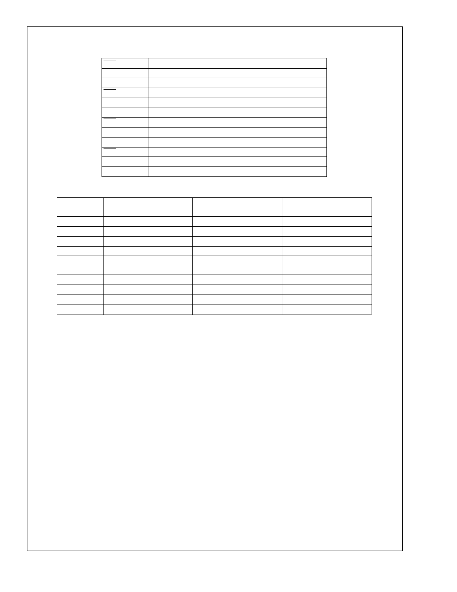
TABLE 1. Logic Table for Loopback Controls
LB0
Loopback Function
0
Enable loopback from IB_0
±
to OA_0
±
.
1 (default)
Normal mode. Loopback disabled.
LB1
Loopback Function
0
Enable loopback from IB_1
±
to OA_1
±
.
1 (default)
Normal mode. Loopback disabled.
LB2
Loopback Function
0
Enable loopback from IB_2
±
to OA_2
±
.
1 (default)
Normal mode. Loopback disabled.
LB3
Loopback Function
0
Enable loopback from IB_3
±
to OA_3
±
.
1 (default)
Normal mode. Loopback disabled.
TABLE 2. De-Emphasis Controls
PreA_[1:0]
Default VOD Level in mV
PP
(VODB)
De-Emphasis Level in mV
PP
(VODPE)
De-Emphasis in dB
(VODPE/VODB)
0 0
1200
1200
0
0 1
1200
850
-3
1 0
1200
600
-6
1 1 (Default)
1200
426
-9
PreB_[1:0]
Default VOD Level in mV
PP
(VODB)
De-Emphasis Level in mV
PP
(VODPE)
De-Emphasis in dB
(VODPE/VODB)
0 0
1200
1200
0
0 1
1200
850
-3
1 0
1200
600
-6
1 1 (Default)
1200
426
-9
De-emphasis is the primary signal conditioning function for
use in compensating against backplane transmission loss.
The DS25BR400 provides four steps of de-emphasis rang-
ing from 0, -3, -6 and -9 dB, user-selectable dependent on
the loss profile of the backplane. Figure 1 shows a driver
de-emphasis waveform. The de-emphasis duration is nomi-
nal 188 ps, corresponding to 0.75 bit-width at 2.5 Gbps. The
de-emphasis levels of switch-side and line-side can be indi-
vidually programmed.
DS25BR400
www.national.com
5