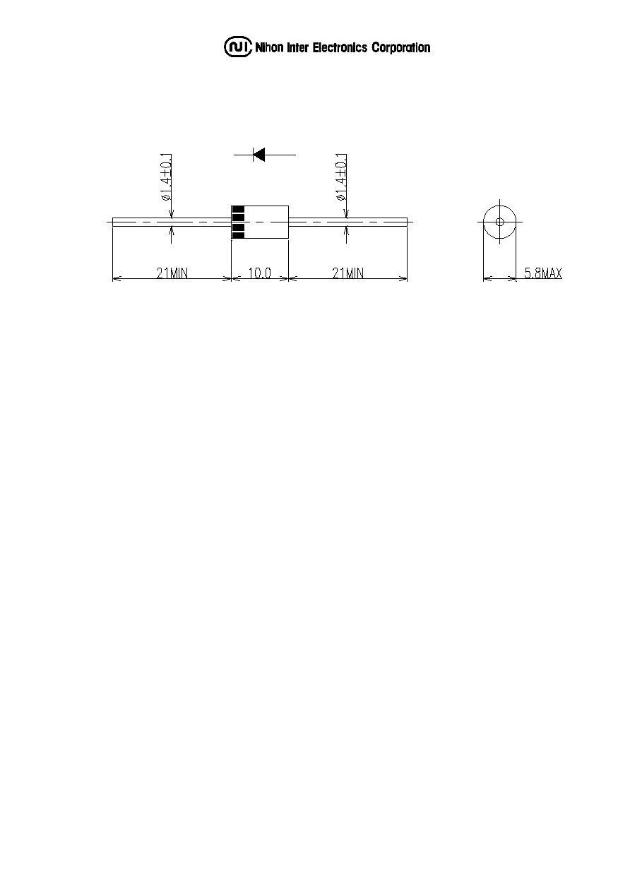
OUTLINE DRAWING
Maximum Ratings
Approx Net Weight:1.18g
Rating
Symbol 31DQ06 Unit
Repetitive Peak Reverse Voltage
V
RRM
60
V
Non-repetitive Peak Reverse Voltage
V
RSM
65 V
Without Fin or
P.C.Board
1.6 Ta=25
∞
C
Average Rectified
Output Current
With Fin *1
I
O
3.0 Ta=43
∞
C
Half Sine Wave Resistive Load A
RMS Forward Current
I
F(RMS)
4.71 A
Surge Forward Current
I
FSM
75 Half Sine Wave,1cycle,Non-repetitive
A
Operating JunctionTemperature Range
Tjw
- 40 to + 150
∞
C
Storage Temperature Range
Tstg
- 40 to + 150
∞
C
Electrical
∑
Thermal Characteristics
Characteristics
Symbol
Conditions Min
Typ
Max
Unit
Peak Reverse Current
I
RM
Tj= 25
∞
C, V
RM
= V
RRM
- - 3 mA
Peak Forward Voltage
V
FM
Tj= 25
∞
C, I
FM
= 3 A
- - 0.58 V
Without Fin or P.C.Board
80
Thermal Resistance(Junction to Ambient) Rth(j-a)
With Fin *1
- -
34
∞
C/W
*1 :20x20x1t(mm) Copper plates, L=5mm, Both Sides
SBD
Type :
Type :
Type :
Type :
31
31
31
31D
D
D
DQ06
Q06
Q06
Q06
FEATURES
* Low Forward Voltage Drop
* Low Power Loss, High Efficiency
* High Surge Capability
* 30volts trough 100volts Types Available