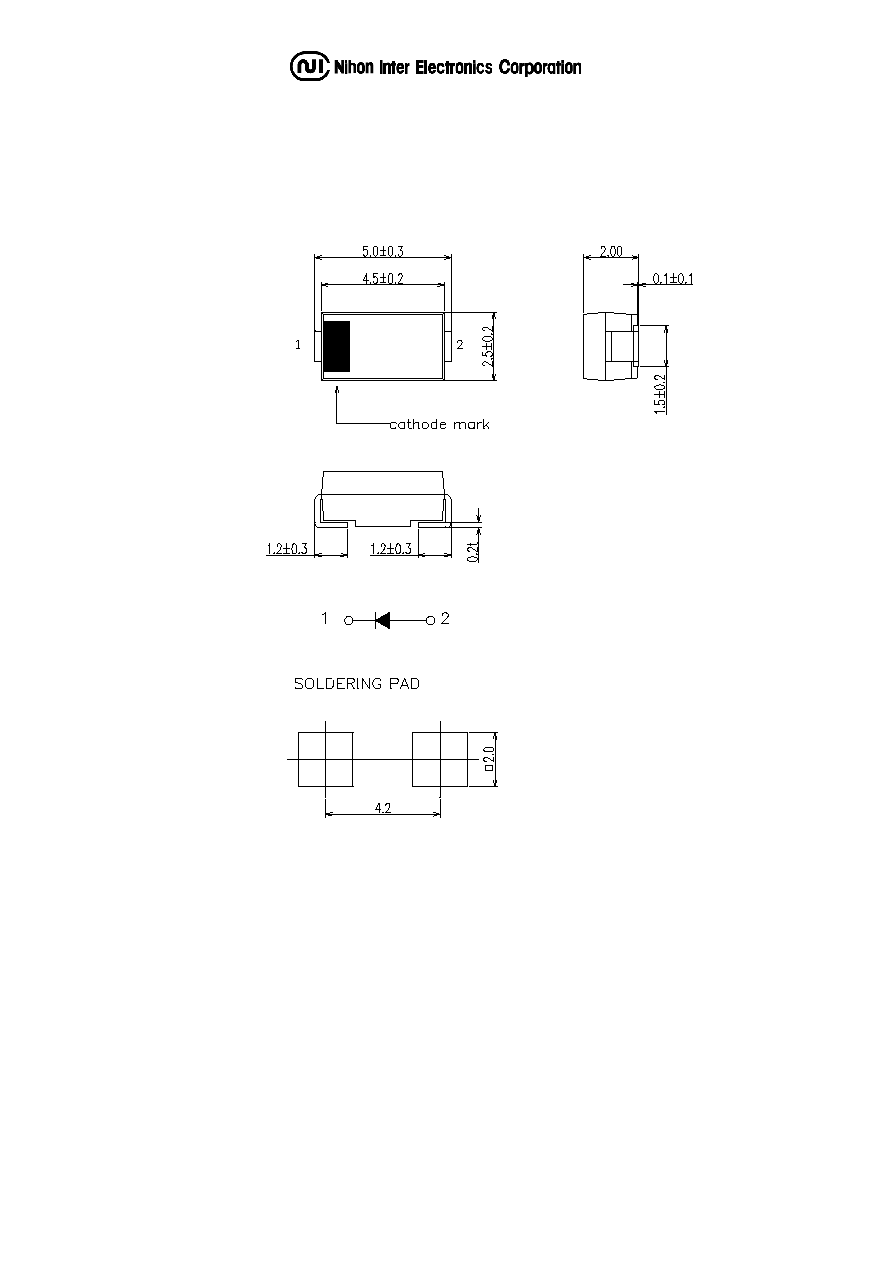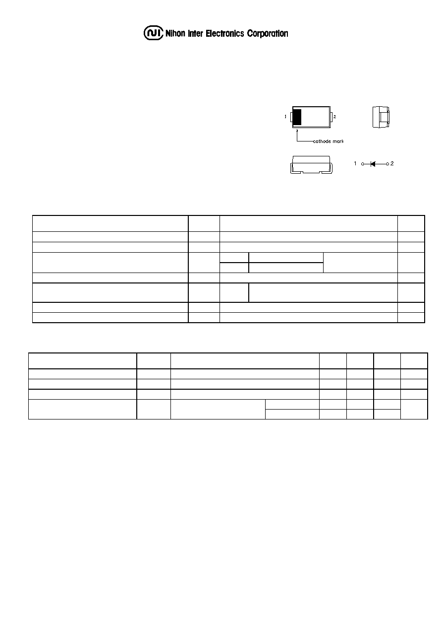
OUTLINE DRAWING
Maximum Ratings
Approx Net Weight:0.06g
Rating Symbol EC10DA40 Unit
Repetitive Peak Reverse Voltage
V
RRM
400
V
Non-repetitive Peak Reverse Voltage
V
RSM
450
V
0.76 Ta=25
∞
C *1
Average Rectified Output Current
I
O
1.0 Ta=29
∞
C *2
50Hz Half Sine
Wave Resistive Load
A
RMS Forward Current
I
F(RMS)
1.57
A
Surge Forward Current
I
FSM
25
50Hz Half Sine Wave,1cycle
Non-repetitive
A
Operating JunctionTemperature Range
T
jw
-40 to +150
∞
C
Storage Temperature Range
T
stg
-40 to +150
∞
C
Electrical
∑
Thermal Characteristics
Characteristics Symbol
Conditions
Min.
Typ.
Max.
Unit
Peak Reverse Current
I
RM
Tj= 25
∞
C, V
RM
= V
RRM
- - 10
µ
A
Peak Forward Voltage
V
FM
Tj= 25
∞
C, I
FM
= 1.0A
- -
1.05
V
Electrostatic Discharge
-
Tj= 25
∞
C, C = 150 pF, R = 150 ohm *3
- 25 - kV
*1 -
-
157
Thermal Resistance
Rth
(j-a)
Junction to Ambient
*2 -
-
108
∞
C
/W
*1 Glass Epoxy Substrate Mounted (Soldering Lands=2x2mm,Both Sides)
*2 Alumina Substrate Mounted (Soldering Lands=2x2mm,Both Sides)
*3 Mesured by ESS-630S of NOISE LABORATORY
DIODE
Type
:
EC10DA40
EC10DA40
EC10DA40
EC10DA40
Electrostatic Discharge Reinforcement Type
Electrostatic Discharge Reinforcement Type
Electrostatic Discharge Reinforcement Type
Electrostatic Discharge Reinforcement Type
FEATURES
FEATURES
FEATURES
FEATURES
* Miniature Size,Surface Mount Device
* High Surge Capability
* Low Forward Voltage Drop
* Low Reverse Leakage Current
* Packaged in 12mm Tape and Reel