THYRISTOR MODULE
Maximum Ratings
Approx Net Weight:155g
Grade
Parameter
Parameter
Parameter
Parameter
Symbol
PAT/PAH3012 PAT/PAH3016
Unit
Repetitive Peak Off-State Voltage
V
DRM
1200
1600
Non Repetitive Peak Off-State Voltage
V
DSM
1300
1700
V
Parameter
Parameter
Parameter
Parameter
Conditions
Conditions
Conditions
Conditions
Max Rated
Max Rated
Max Rated
Max Rated
Value
Value
Value
Value
Unit
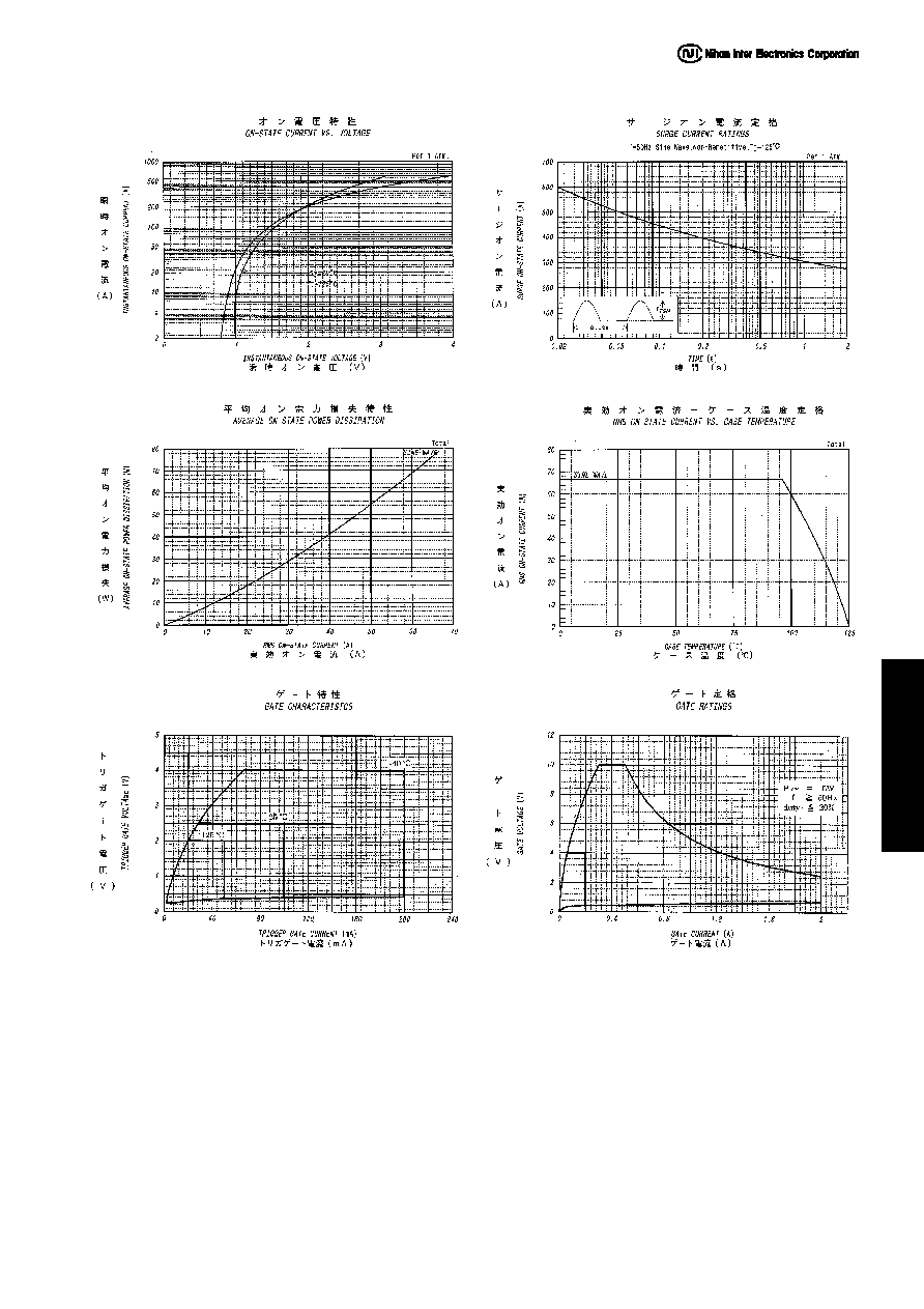
RMS On-State Current
I
T(RMS)
50Hz Half Sine Wave condition
Tc=96
∞
C
66 A
Surge On-State Current
I
FSM
50 Hz Half Sine Wave,1Pulse
Non-Repetitive
600 A
I Squared t
I
2
t
2msec to 10msec
1800
A
2
s
Critical Rate of Turned-On Current
di/dt
V
D
=2/3V
DRM
, I
TM
=2
∑
I
O
, Tj=125
∞
C
I
G
=200mA, di
G
/dt=0.2A/
µ
s
100
A/
µ
s
Peak Gate Power
P
GM
5
W
Average Gate Power
P
G(AV)
1
W
Peak Gate Current
I
GM
2
A
Peak Gate Voltage
V
GM
10
V
Peak Gate Reverse Voltage
V
RGM
5
V
Operating JunctionTemperature Range
Tjw
-40 to +125
∞
C
Storage Temperature Range
Tstg
-40 to +125
∞
C
Isoration Voltage
Viso
Base Plate to Terminals, AC1min
2500 V
Case mounting
M6 Screw
2.4 to 3.5
Mounting torque
Terminals
Ftor
M5 Screw
2.4 to 2.8
N
∑
m
Value per 1 Arm
FEATURES
* Isolated Base
* Dual Thyristors or Thyristor and
Diode Anti-Parallel Circuit
* High Surge Capability
* UL Recognized, File No. E187184
TYPICAL APPLICATIONS
* AC phase control
* AC switch
P A T 3 0 1 2 P A T 3 0 1 6
P A T 3 0 1 2 P A T 3 0 1 6
P A T 3 0 1 2 P A T 3 0 1 6
P A T 3 0 1 2 P A T 3 0 1 6
P A H 3 0 1 2 P A H 3 0 1 6
P A H 3 0 1 2 P A H 3 0 1 6
P A H 3 0 1 2 P A H 3 0 1 6
P A H 3 0 1 2 P A H 3 0 1 6
OUTLINE DRAWING
66A / 1200 to 1600V
PAT
PAH

Electrical
∑
Thermal Characteristics
Maximum Value.
Characteristics
Symbol
Test Conditions
Min. Typ. Max.
Unit
Peak Off-State Current
I
DM
V
DM
= V
DRM,
Tj=125
∞
C
20
mA
Peak On-State Voltage
V
TM
I
TM
= 90A, Tj=25
∞
C
1.50
V
Tj=-40
∞
C
200
Tj=25
∞
C
100
Gate Current to Trigger
I
GT
V
D
=6V,I
T
=1A
Tj=125
∞
C
50
mA
Tj=-40
∞
C
4
Tj=25
∞
C
2.5
Gate Voltage to Trigger
V
GT
V
D
=6V,I
T
=1A
Tj=125
∞
C
2
V
Gate Non-Trigger Voltage
V
GD
V
D
=2/3V
DRM
Tj=125
∞
C
0.25 V
Critical Rate of Rise of Off-State
Voltage
dv/dt V
D
=2/3V
DRM
Tj=125
∞
C
500 V/
µ
s
Turn-Off Time
tq
I
TM
=I
O
,V
D
=2/3V
DRM
dv/dt=20V/
µ
s, V
R
=100V
-di/dt=20A/
µ
s, Tj=125
∞
C
100
µ
s
Turn-On Time
tgt
6
µ
s
Delay Time
td
2
µ
s
Rise Time
tr
Tj=25
∞
C, I
TM
=I
T(RMS)
V
D
=100V, I
G
=200mA
di
G
/dt=0.2A/
µ
s
4
µ
s
Latching Current
I
L
Tj=25
∞
C
100 mA
Holding Current
I
H
Tj=25
∞
C
50
Rth(j-c) Junction to Case
0.35
Thermal Resistance *1
Rth(c-f)
Base Plate to Heat Sink
with Thermal Compound
0.1
∞
C/W
Value Per 1Arm
*1: Value Per Module