MOSFET
MODULE
Single 560A /150V
Single 560A /150V
Single 560A /150V
Single 560A /150V
PHM5601
PHM5601
PHM5601
PHM5601
MAXMUM RATINGS
Ratings Symbol PHM5601 Unit
Drain-Source Voltage (V
GS
=0V) V
DSS
150 V
Gate - Source Voltage
V
GSS
+/ - 20
V
Duty=50% 560
(Tc=25
�
C)
Continuous Drain Current
D.C.
I
D
440 (Tc=25
�
C)
A
Pulsed Drain Current
I
DM
1,120
Tc=25
�
C) A
Total Power Dissipation
P
D
1,780
Tc=25
�
C) W
Operating Junction Temperature Range
T
jw
-40 to +150
�
C
Storage Temperature Range
T
stg
-40 to +125
�
C
Isolation Voltage Terminals to Base AC, 1 min.)
V
ISO
2,500
V
Module Base to Heatsink
3.0
Gate Terminals
M4
1.4
Mounting Torque
Bus Bar to Main Terminals
F
TOR
M8 10.5
N
�
m
ELECTRICAL CHARACTERISTICS
(@Tc=25
�
C unless otherwise noted)
Characteristic Symbol
Test
Condition
Min.
Typ.
Max.
Unit
Zero Gate Voltage Drain Current
I
DSS
V
DS
=V
DSS
,V
GS
=0V -
-
3.2
mA
Gate-Source Leakage Current
I
GSS
V
GS
=+/- 20V,V
DS
=0V -
-
3.2
�
A
Gate-Source Threshold Voltage
V
GS(th)
V
DS
=V
GS
, I
D
=16mA 1.0
2.0
3.2
V
Static Drain-Source On-Resistance
r
DS(on)
V
GS
=10V, I
D
=560A -
1.6
2.0
m-ohm
Drain-Source On-Voltage
V
DS(on)
V
GS
=10V, I
D
=560A -
1.0
1.2
V
Forward Transconductance
g
fs
V
DS
=15V, I
D
=560A -
-
-
S
Input Capacitance
C
ies
-
110
-
nF
Output Capacitance
C
oss
-
13
-
nF
Reverse Transfer Capacitance
C
rss
V
DS
=10V,V
GS
=0V,f=1MHz
- 13 -
nF
Rise Time
t
r
-
400
-
Turn-On Delay Time
t
d(on)
-
380
-
Fall Time
t
f
- 170 -
Turn-Off Delay Time
t
d(off)
V
DD
= 80V
I
D
=280A
V
GS
= -5V, +10V
R
G
= 1.2 ohm
- 1,100 -
ns
FREE WHEELING DIODES RATINGS & CHARACTERISTICS
(Tc=25
�
C)
Characteristic Symbol Test
Condition Min.
Typ.
Max.
Unit
Duty=50%. -
-
560
Continuous Source Current
I
S
D.C. (Terminal Temperature=80
�
C
450
A
Pulsed Source Current
I
SM
- -
-
1,120
A
Diode Forward Voltage
V
SD
I
S
=560A -
1.6
2.0
V
Reverse Recovery Time
t
rr
I
S
=560A, -dis/dt=1,100A/
�
s
- 130 -
ns
THERMAL CHRACTERISTICS
Characteristic Symbol Test
Condition Min.
Typ.
Max.
Unit
Thermal Resistance, Junction to Case
R
th(j-c)
-
- 0.07
Thermal Resistance, Case to Heatsink
R
th(c-f)
Mounting surface flat, smooth, and greased
-
-
0.035
�
C/W
FEATURES
* Trench Gate MOS FET Module
* Super Low Rds(ON) 2 milliohms( @560A )
* With Fast Recovery Source-Drain Diode
TYPICAL APPLICATIONS
* Chopper Control For FORKLIFTs
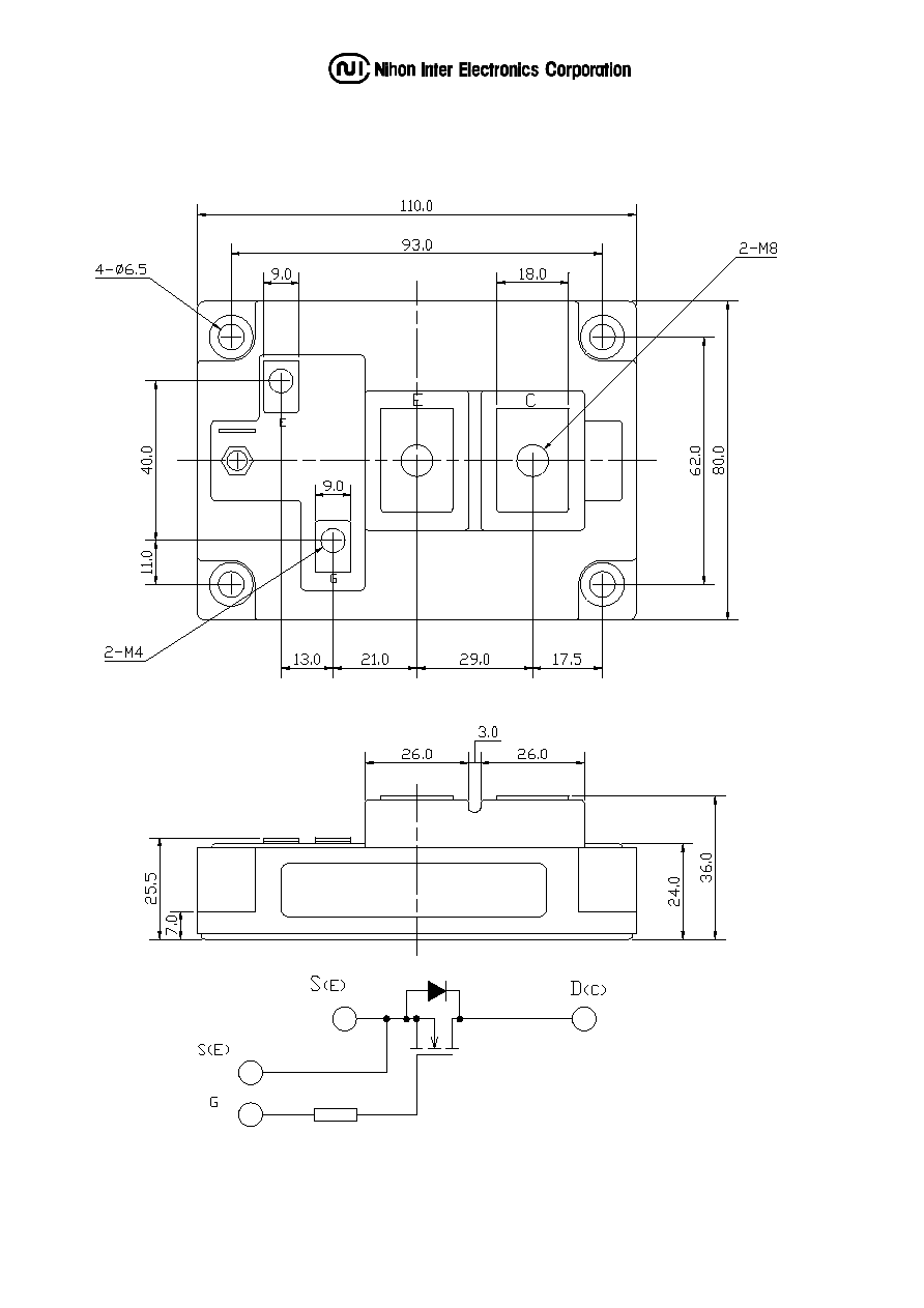
Approximate Weight : 650g
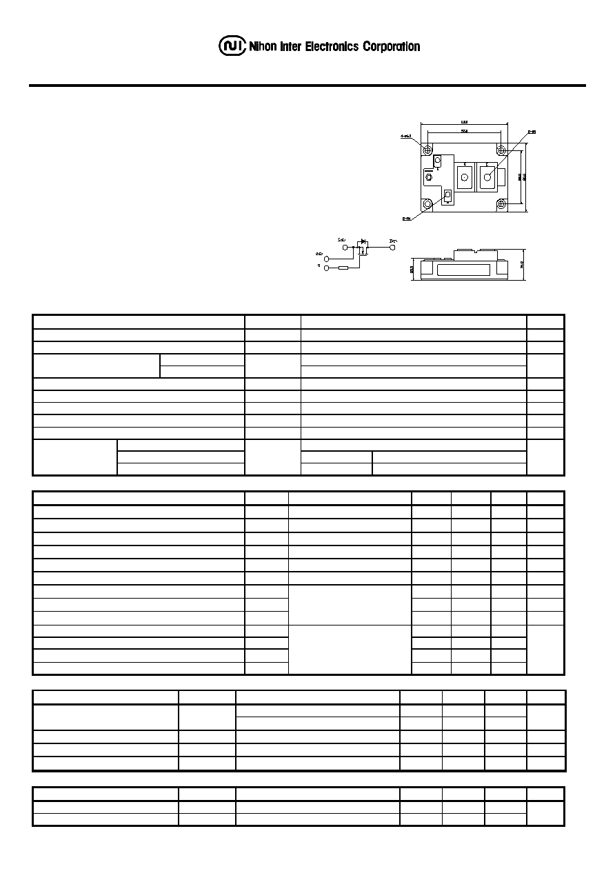
OUTLINE DRAWING
Circuit
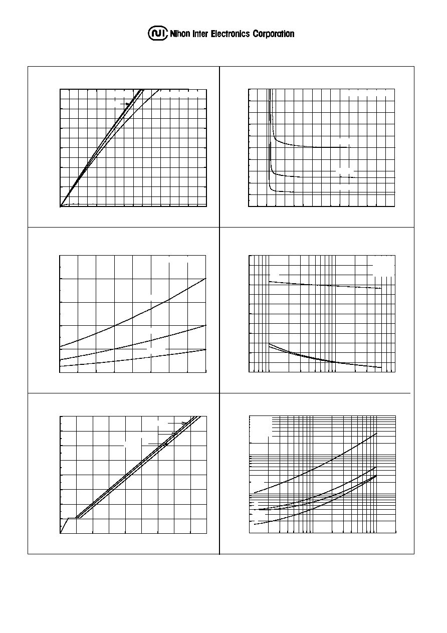
0
0.5
1
1.5
2
2.5
3
3.5
4
0
200
400
600
800
1000
1200
Drain to Source Voltage V
DS
(V)
D
r
a
i
nCu
r
r
ent
I
D
(A
)
Fig.1- Output Characteristics
(Typical)
T
C
=25
4V
V
GE
=10V
3V
2V
8V
250s PULSE TEST
0
2
4
6
8
10
12
14
16
0
0.2
0.4
0.6
0.8
1
1.2
1.4
1.6
1.8
2
Gate to Source Voltage V
GS
(V)
D
r
a
i
n
t
o
S
o
ur
ce V
o
l
t
a
g
e
V
DS
(V
)
Fig.2- Drain to Source On Voltage
vs. Gate to Source Voltage
(Typical)
T
C
=25
I
D
=140A
I
D
=280A
I
D
=560A
250s PULSE TEST
-50
0
50
100
150
0
0.5
1
1.5
2
2.5
Junction Temperature Tj
()
D
r
a
i
n
t
o
S
o
ur
ce V
o
l
t
a
g
e
V
DS
(V
)
Fig.3- Drain to Source On Voltage
vs. Junction Temperature
(Typical)
V
GS
=10V
I
D
=140A
I
D
=280A
I
D
=560A
250s PULSE TEST
0
500
1000
1500
2000
2500
3000
3500
4000
4500
0
2
4
6
8
10
12
14
16
Total Gate Charge Qg
(nC)
G
a
t
e
t
o
S
o
ur
ce V
o
l
t
a
g
e
V
GS
(V
)
Fig.5- Gate Charge vs. Gate to Source Voltage
(Typical)
V
DD
=80V
I
D
=560A
V
DD
=40V
V
DD
=20V
1
2
5
10
20
50
100
200
0.1
0.2
0.5
1
2
5
10
20
50
100
Series Gate Impedance R
G
()
Sw
i
t
chi
ng
T
i
m
e
t
(
s)
Fig.6- Series Gate Impedance vs. Switching Time
(Typical)
V
DD
=80V
I
D
=280A
T
C
=25
tf
tr
td(on)
td(off)
0.5
1
2
5
10
20
50
80
0
25000
50000
75000
100000
125000
150000
Drain to Source Voltage V
DS
(V)
C
a
pa
ci
t
a
nce C
(n
F
)
Fig.4- Capacitance vs. Drain to Source Voltage
(Typical)
Ciss
Coss
Crss
V
GS
=0V
f=1MH
Z
T
C
=25
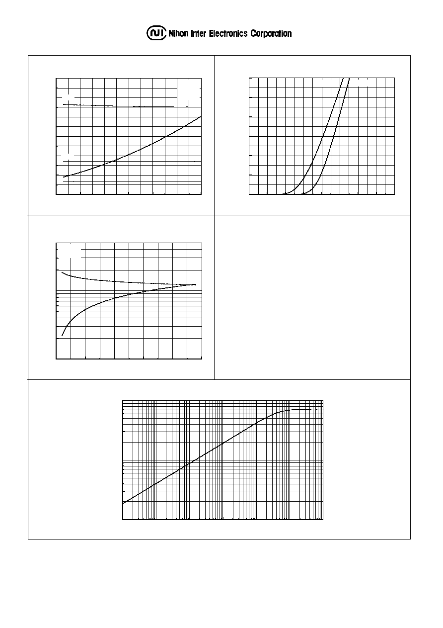
0
100
200
300
400
500
600
0
0.2
0.4
0.6
0.8
1
1.2
Drain Current I
D
(A)
S
w
i
t
chi
n
g
T
i
m
e
t
(
s)
Fig.7- Drain Current vs. Switching Time
(Typical)
td(off)
tf
t
r
td(on)
V
DD
=80V
R
G
=1.2
T
C
=25
0
0.2
0.4
0.6
0.8
1
1.2
1.4
1.6
0
200
400
600
800
1000
1200
Source to Drain Voltage V
SD
(V)
S
o
ur
ce Cur
r
ent
I
S
(A
)
Fig.8- Source to Drain Diode
Forward
Characteristics
(Typical)
T
J
=125
T
J
=25
0
500
1000
1500
2000
2500
10
20
50
100
200
500
-di/dt
(A/s)
P
e
a
k
R
e
v
e
r
s
e
R
eco
v
e
r
y
Cur
r
ent
I
Rr
M
(A
)
R
e
v
e
r
s
e
R
eco
v
e
r
y
T
i
m
e
t
r
r
(n
s
)
Fig.9- Reverse Recovery Characteristics
(Typical)
I
RrM
trr
-I
S
=800A
T
J
=125
10
-5
10
-4
10
-3
10
-2
10
-1
1
10
1
1x10
-3
3x10
-3
1x10
-2
3x10
-2
1x10
-1
SQUARE WAVE PULSE DURATION t
(s)
T
r
a
n
s
i
e
n
t
T
h
er
m
a
l
I
m
peda
nc
e
R
t
h
(J-
C
)
(
/W
)
Fig.10- Maximun Transient Thermal Impedance