NJG1110PB1
- 1 -
PDC Dual Band LNA GaAs MMIC
n
GENERAL DESCRIPTION
n
PACKAGE OUTLINE
The NJG1110PB1 is a dual band low noise amplifier (2 input
2 output) GaAs MMIC for 800MHz and 1500MHz band. The
band switching between 800MHz and 1500MHz is established
by one bit control signal by using built-in inverter circuit.
An ultra small & thin FFP12 (
Flip-Chip Fine package
) package
is adopted.
n
FEATURES
l
Low voltage operation
+2.8V typ.
l
Low current consumption
2.7mA typ.
l
Low control current
20uA typ.
l
High gain
18dB typ. @f=820MHz
16dB typ. @f=1490MHz
l
Low noise figure
1.2dB typ. @f=820MHz
1.1dB typ. @f=1490MHz
l
High output IP3
+10dBm typ. @f=820MHz
+13dBm typ. @f=1490MHz
l
Ultra small & ultra thin package
FFP12-B1 (Package size: 2.0x2.0x0.85mm)
n
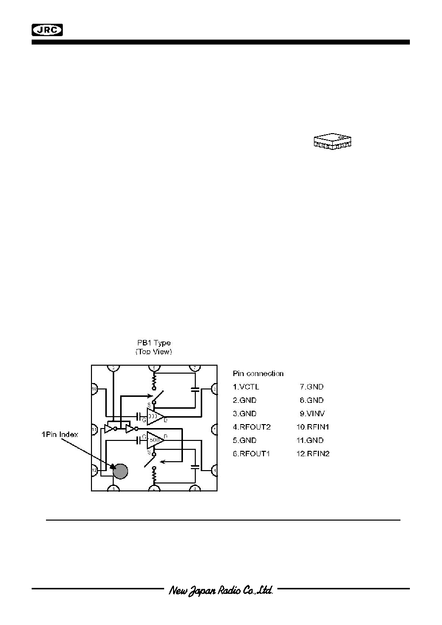
PIN CONFIGURATION
Note: The specifications and description listed in this catalog are subject to change without prior notice.
NJG1110PB1
NJG1110PB1
- 2 -
n
ABSOLUTE MAXIMUM RAT INGS
(T
a
=25∞C, Z
s
=Z
l
=50
)
PARAMETERS
SYMBOL
CONDITIONS
RATINGS
UNITS
Operating voltage
V
DD
5.0
V
Control voltage
V
CTL
5.0
V
Inverter supply voltage
V
INV
5.0
V
Input power
Pin
V
DD
=2.8V
+15
dBm
Power dissipation
P
D
300
mW
Operating temperature
T
opr
-40~+85
∞C
Storage temperature
T
stg
-55~+125
∞C
n
ELECTRICAL CHARACTERISTICS 1 (DC)
(T
a
=+25∞C, Z
s
=Z
l
=50
, V
DD
=V
INV
=2.8V)
PARAMETERS
SYMBOL
CONDITIONS
MIN
TYP
MAX UNITS
Operating voltage
V
DD
2.5
2.8
4.5
V
Inverter supply voltage
V
INV
2.5
2.8
4.5
V
Control voltage (High)
V
CTL(H)
2.0
2.8
V
INV
V
Control voltage (Low)
V
CTL(L)
0.0
0.0
0.8
V
No RF signal, V
CTL
=V
CTL(L)
-
2.7
3.25
mA
Operating current
I
DD
No RF signal, V
CTL
=V
CTL(H)
-
2.7
3.25
mA
Control current
I
CTL
No RF signal
-
20
60
uA
Inverter current
I
INV
No RF signal
-
100
200
uA
NJG1110PB1
- 3 -
n
ELECTRICAL CHARACTERISTICS 2 (800MHz BAND RF)
(T
a
=+25∞C, Z
s
=Z
l
=50
, V
DD
=V
INV
=2.8V, V
CTL
=V
CTL(L)
, freq=810~885MHz, with application circuit)
PARAMETERS
SYMBOL
CONDITIONS
MIN
TYP
MAX UNITS
Small signal gain
Gain1
16.0
18.0
19.0
dB
G
flat1
freq=810~830MHz
-
-
0.5
dB
G
flat2
freq=838~843MHz
-
-
0.5
dB
Gain flatness
G
flat3
freq=870~885MHz
-
-
0.5
dB
Noise figure
NF1
-
1.2
1.4
dB
Pin at 1dB
compression point
P
-1dB(IN)1
-21
-18
-
dBm
Output 3rd order
intercept point
OIP3_1 f1=freq, f2=freq+100kHz
Pin=-35dBm
+6
+10
-
dBm
ISL1
freq=680~780MHz
25
30
-
dB
ISL2
freq=1360~1560MHz
35
45
-
dB
Isolation
ISL3
freq=2040~2340MHz
45
55
-
dB
Image suppression ratio
IMR1
freq=582.4~657.4MHz
4
6
-
dB
RF INPUT1 VSWR
VSWR
i
1
-
-
2.2
-
RF OUTPUT1 VSWR
VSWR
o
1
-
-
2.0
-
n
ELECTRICAL CHARACTERISTICS 3 (1.5GHz BAND RF)
(T
a
=+25∞C, Z
s
=Z
l
=50
, V
DD
=V
INV
=2.8V, V
CTL
=V
CTL(H)
, freq=1477~1501MHz, with application circuit)
PARAMETERS
SYMBOL
CONDITIONS
MIN
TYP
MAX UNITS
Small signal gain
Gain2
15.0
16.0
17.0
dB
Gain flatness
G
flat4
freq=1477~1501MHz
-
-
0.5
dB
Noise figure
NF2
-
1.1
1.25
dB
Pin at 1dB
compression point
P
-1dB(IN)2
-20
-17
-
dBm
Output 3rd order
intercept point
OIP3_2 f1=freq, f2=freq+100kHz
Pin=-35dBm
+6
+13
-
dBm
ISL4
freq=1580~1620MHz
25
30
-
dB
ISL5
freq=3160~3240MHz
40
50
-
dB
Isolation
ISL6
freq=4740~4860MHz
30
40
-
dB
Image suppression ratio
IMR2
freq=1700~1729MHz
3
5
-
dB
RF INPUT2 VSWR
VSWR
i
2
-
-
2.1
-
RF OUTPUT2 VSWR
VSWR
o
2
-
-
2.0
-

NJG1110PB1
- 4 -
n
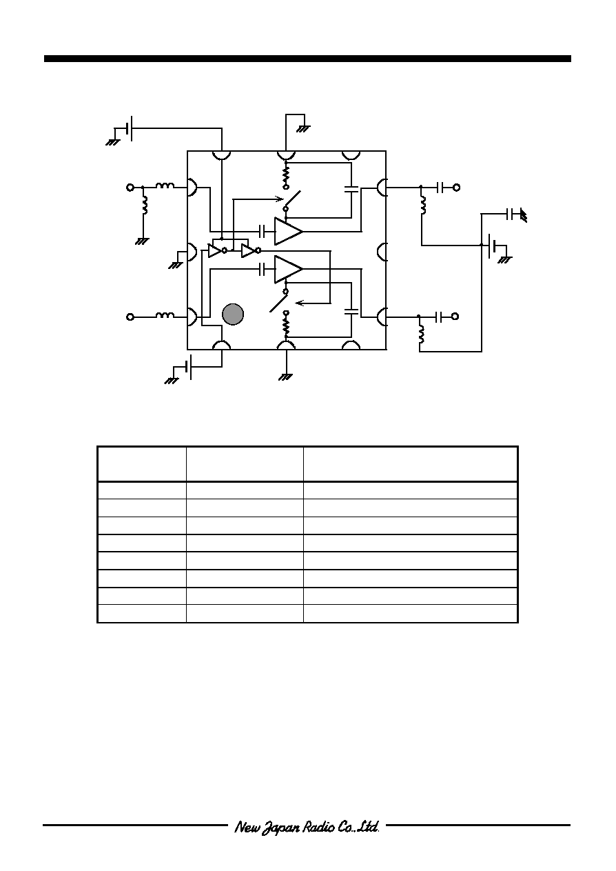
TERMINAL INFORMATION
Pin
Symbol
Description
1
VCTL
Control Voltage terminal to select 800MHz band or 1.5GHz band to
celect.
2
GND
Ground terminal (0V).
3
GND
Ground terminal (0V).
4
RFOUT2
Output terminal of 1.5GHz band. This terminal is also the power supply
terminal of the LNA, please use inductor (L5) to connect power supply.
(Please see application circuit.)
5
GND
Ground terminal (0V).
6
RFOUT1
Output terminal of 800MHz band. This terminal is also the power supply
terminal of the LNA, please use inductor (L3) to connect power supply.
(Please see application circuit.)
7
GND
Ground terminal (0V).
8
GND
Ground terminal (0V).
9
VINV
Power supply terminal of the inverter circuit.
10
RFIN1
Output terminal of 800MHz band. The DC blocking capacitor is not
required.
11
GND
Ground terminal (0V).
12
RFIN2
Output terminal of 1.5GHz band. The DC blocking capacitor is not
required.
NOTE:
1) Ground terminal (2, 3, 5, 8, 11pin) should be connected to ground plane by multiple via
holes for good grounding.
2)
Please connect bypass capacitors possible close to inductors (L3, L5)..
NJG1110PB1
- 5 -
n
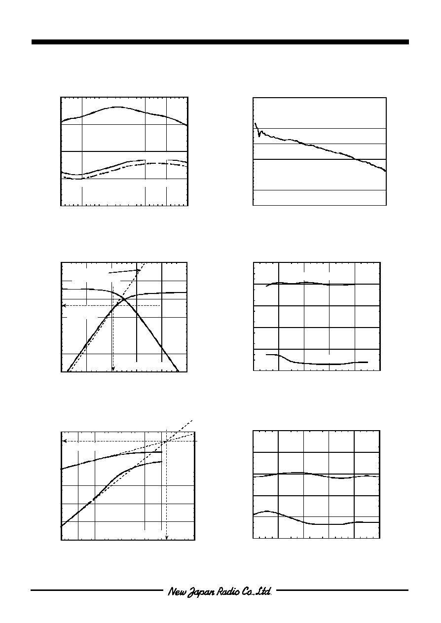
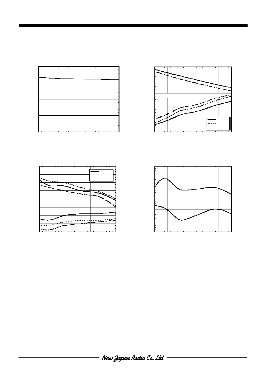
TYPICAL CHARACTERISTICS (800MHz Band)
-0.50
-0.40
-0.30
-0.20
-0.10
0.00
0.10
0.20
0
500
1000
1500
2000
2500
3000
Input Line Loss 800MHz Band
INPUT LINE LOSS ( dB )
freq ( MHz )
-100
-80
-60
-40
-20
0
20
-40
-35
-30
-25
-20
-15
-10
-5
0
Pout,IM3 vs. Pin
Pout,IM3 (dBm)
Pin (dBm)
( V
DD
=V
INV
=2.8V,V
CTL
=0V,I
DD
=2.6mA,f=820+820.1MHz,Ta=25
o
C )
IIP3=-7.8dBm
IM3
Pout
OIP3=+9.9dBm
-10
-8
-6
-4
-2
0
4
6
8
10
12
14
800
820
840
860
880
900
IIP3,OIP3 vs. freq
IIP3 (dBm)
OIP3 (dBm)
freq (MHz)
( V
DD
=V
INV
=2.8V,V
CTL
=0V,I
DD
=2.6mA,df=100kHz,P
RF
=-36dBm,Ta=25
o
C )
IIP3
OIP3
-20
-15
-10
-5
0
5
10
-5
0
5
10
15
20
25
-40
-30
-20
-10
0
10
Pout vs. Pin,Gain
Pout (dBm)
Gain (dB)
( V
DD
=2.8V,V
CTL
=0V,I
DD
=2.6mA,freq=820MHz,Ta=25
o
C )
P-1dB(OUT)
=-1.8dBm
Gain
Pout
P-1dB(IN)=-18.5dBm
1dB Gain
Compression Line
Pin (dBm)
-20
-18
-16
-14
-12
-10
-10
-8
-6
-4
-2
0
800
820
840
860
880
900
P-1dB(IN),P-1dB(OUT) vs. freq
P-1dB(IN) (dBm)
P-1dB(OUT) (dBm)
freq (MHz)
( V
DD
=V
INV
=2.8V,V
CTL
=0V,I
DD
=2.6mA,,Ta=25
o
C )
P-1dB(IN)
P-1dB(OUT)
0.5
1.0
1.5
2.0
2.5
0
5
10
15
20
700
750
800
850
900
950
1000
NF,Gain vs. freq
NF (dB)
Gain (dB)
freq (MHz)
( V
DD
=V
INV
=2.8V,V
CTL
=0V,I
DD
=2.6mA,Ta=25
o
C )
Gain
NF(Embedded PCB,Connector LOSS)
NF(De-embedded PCB,Connector LOSS)

NJG1110PB1
- 6 -
n
TYPICAL CHARACTERISTICS (800MHz Band)
14
15
16
17
18
19
1.1
1.2
1.3
1.4
1.5
1.6
2.0
2.5
3.0
3.5
4.0
4.5
5.0
Gain,NF vs. VDD
Gain ( dB )
NF ( dB )
VDD ( V )
Gain
NF(De-embedded PCB,Connector LOSS)
Max (810 to 885MHz)
Max (810 to 885MHz)
Min (810 to 885MHz)
Min (810 to 885MHz)
( V
INV
=2.8V,V
CTL
=0V,freq=810 to 885MHz )
4
5
6
7
8
9
10
11
12
-11
-10
-9
-8
-7
-6
-5
-4
-3
2.0
2.5
3.0
3.5
4.0
4.5
5.0
OIP3,IIP3 vs. VDD
OIP3 ( dBm )
IIP3 ( dBm )
VDD ( V )
OIP3
IIP3
Max (810 to 885MHz)
Max (810 to 885MHz)
Min (810 to 885MHz)
Min (810 to 885MHz)
( V
INV
=2.8V,V
CTL
=0V,freq=810 to 885MHz )
-7
-6
-5
-4
-3
-2
-1
0
1
-22
-21
-20
-19
-18
-17
-16
-15
-14
2.0
2.5
3.0
3.5
4.0
4.5
5.0
P-1dB(OUT),P-1dB(IN)
P-1dB(OUT) ( dBm )
P-1dB(IN) ( dBm )
VDD ( V )
P-1dB(OUT)
P-1dB(IN)
( V
INV
=2.8V,V
CTL
=0V,freq=820MHz )
1.0
1.5
2.0
2.5
3.0
2.0
2.5
3.0
3.5
4.0
4.5
5.0
IDD vs. VDD
IDD ( mA )
VDD ( V )
( V
INV
=2.8V,V
CTL
=0V,freq=820MHz )
NJG1110PB1
- 7 -
n
TYPICAL CHARACTERISTICS (800MHz Band)
10
12
14
16
18
20
0.4
0.8
1.2
1.6
2.0
2.4
-40
-20
0
20
40
60
80
Gain,NF vs. Ta
f=810MHz
f=840MHz
f=885MHz
Gain (dB)
NF (dB)
Ta (
o
C)
( V
DD
=V
INV
=2.8V,V
CTL
=0V,IDD=2.6mA )
Gain
NF(De-embedded PCB,Connector LOSS)
7.0
7.5
8.0
8.5
9.0
9.5
10.0
10.5
11.0
-9.0
-8.5
-8.0
-7.5
-7.0
-6.5
-6.0
-5.5
-5.0
-40
-20
0
20
40
60
80
OIP3,IIP3 vs. Ta
f=810MHz
f=840MHz
f=885MHz
OIP3 ( dBm )
IIP3 ( dBm )
Ta (
o
C)
( V
DD
=V
INV
=2.8V,V
CTL
=0V,IDD=2.6mA )
OIP3
IIP3
1.0
1.5
2.0
2.5
3.0
-40
-20
0
20
40
60
80
IDD vs. Ta
IDD (mA)
Ta (
o
C)
( V
DD
=V
INV
=2.8V,V
CTL
=0V,IDD=2.6mA,freq=820MHz )
-6
-5
-4
-3
-2
-1
0
-21
-20
-19
-18
-17
-16
-15
-40
-20
0
20
40
60
80
P-1dB(IN),P-1dB(OUT) vs. Ta
P-1dB(OUT) (dBm)
P-1dB(IN) (dBm)
Ta (
o
C)
( V
DD
=V
INV
=2.8V,V
CTL
=0V,IDD=2.6mA,freq=820MHz )
P-1dB(OUT)
P-1dB(IN)

NJG1110PB1
- 8 -
n
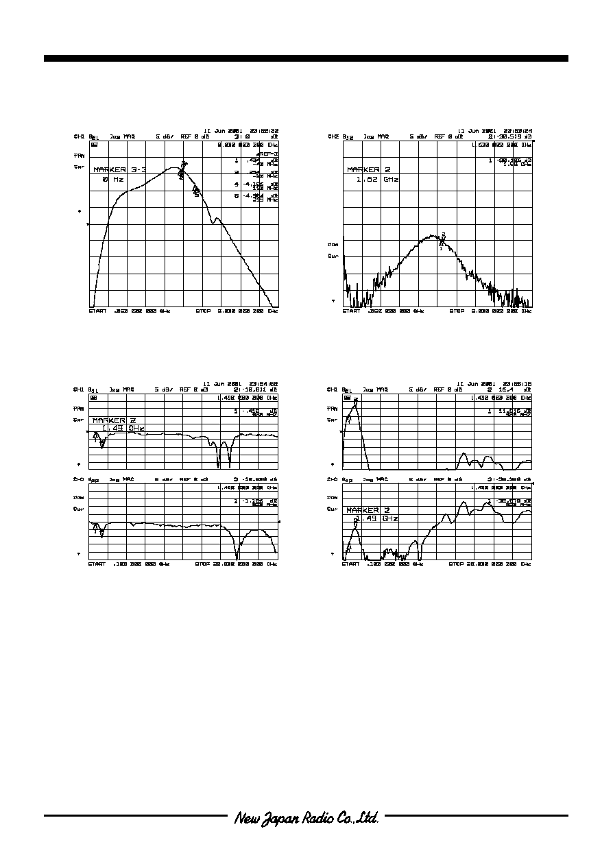
TYPICAL CHARACTERISTICS (800MHz Band)
S11, S22
Zin, Zout
VSWR
S21, 12

NJG1110PB1
- 9 -
n
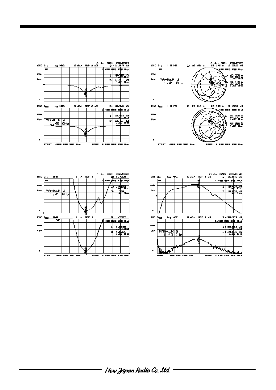
TYPICAL CHARACTERISTICS (800MHz Band)
S11, S22
S21, S12
S12
S21

NJG1110PB1
- 10 -
n
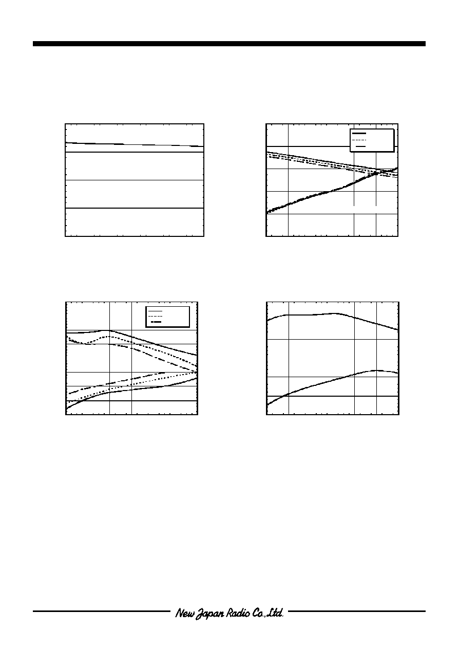
TYPICAL CHARACTERISTICS (1.5GHz Band)
-0.30
-0.25
-0.20
-0.15
-0.10
-0.05
0.00
0
500
1000
1500
2000
2500
3000
Input Line Loss 1500MHz Band
INPUT LINE LOSS ( dB )
freq ( MHz )
0.5
1.0
1.5
2.0
2.5
0
5
10
15
20
1400
1450
1500
1550
1600
NF,Gain vs. freq
NF (dB)
Gain (dB)
freq (MHz)
( V
DD
=V
INV
=V
CTL
=2.8V,I
DD
=2.6mA,Ta=25
o
C )
Gain
NF(Embedded LOSS)
NF(De-embedded LOSS)
-20
-18
-16
-14
-12
-10
-6
-4
-2
0
2
4
1470 1475 1480 1485 1490 1495 1500 1505 1510
P-1dB(IN),P-1dB(OUT) vs. freq
P-1dB(IN) (dBm)
P-1dB(OUT) (dBm)
freq (MHz)
( V
DD
=V
INV
=2.8V,V
CTL
=0V,I
DD
=2.6mA,,Ta=25
o
C )
P-1dB(IN)
P-1dB(OUT)
-100
-80
-60
-40
-20
0
20
-40
-35
-30
-25
-20
-15
-10
-5
0
Pout,IM3 vs. Pin
Pout,IM3 (dBm)
Pin (dBm)
( V
DD
=V
INV
=V
CTL
=2.8V,I
DD
=2.6mA,f=1490+1490.1MHz,Ta=25
o
C )
IIP3=-5.1dBm
IM3
Pout
OIP3=+11.8dBm
-8
-6
-4
-2
0
2
4
6
8
10
12
14
1460
1470
1480
1490
1500
1510
1520
IIP3,OIP3 vs. freq
IIP3 (dBm)
OIP3 (dBm)
freq (MHz)
( V
DD
=V
INV
=V
CTL
=2.8V,I
DD
=2.6mA,df=100kHz,P
RF
=-36dBm,Ta=25
o
C )
IIP3
OIP3
-20
-15
-10
-5
0
5
10
15
-10
-5
0
5
10
15
20
25
-40
-30
-20
-10
0
10
Pout vs. Pin,Gain
Pout (dBm)
Gain (dB)
( V
DD
=V
CTL
=2.8V,I
DD
=2.6mA,freq=1490MHz,Ta=25
o
C )
P-1dB(OUT)=+0.5dBm
Gain
Pout
P-1dB(IN)=-15.5dBm
1dB Gain
Compression Line
Pin (dBm)

NJG1110PB1
- 11 -
n
TYPICAL CHARACTERISTICS (1.5GHz Band)
1.0
1.5
2.0
2.5
3.0
2.0
2.5
3.0
3.5
4.0
4.5
5.0
IDD vs. VDD
IDD ( mA )
VDD ( V )
( V
INV
=2.8V,V
CTL
=0V,freq=1490MHz )
13
14
15
16
17
18
1.0
1.1
1.2
1.3
1.4
1.5
2.0
2.5
3.0
3.5
4.0
4.5
5.0
Gain,NF vs. VDD
Gain ( dB )
NF ( dB )
VDD ( V )
Gain
NF(De-embedded PCB,Connector LOSS)
Max (1477 to 1501MHz)
Max (1477 to 1501MHz)
Min (1477 to 1501MHz)
Min (1477 to 1501MHz)
( V
INV
=V
CTL
=2.8V,freq=1477 to 1501MHz )
6
7
8
9
10
11
12
13
14
-7
-6
-5
-4
-3
-2
-1
0
1
2.0
2.5
3.0
3.5
4.0
4.5
5.0
OIP3,IIP3 vs. VDD
OIP3 ( dBm )
IIP3 ( dBm )
VDD ( V )
OIP3
IIP3
Max (1477 to 1501MHz)
Max (1477 to 1501MHz)
Min (1477 to 1501MHz)
Min (1477 to 1501MHz)
( V
INV
=V
CTL
=2.8V,freq=1477 to 1501MHz )
-6
-5
-4
-3
-2
-1
0
1
2
-17
-16
-15
-14
-13
-12
-11
-10
-9
2.0
2.5
3.0
3.5
4.0
4.5
5.0
P-1dB(OUT),P-1dB(IN) vs. VDD
P-1dB(OUT) ( dBm )
P-1dB(IN) ( dBm )
VDD ( V )
P-1dB(OUT)
P-1dB(IN)
( V
INV
=V
CTL
=2.8V,freq=1490MHz )
NJG1110PB1
- 12 -
n
TYPICAL CHARACTERISTICS (1.5GHz Band)
9.0
9.5
10.0
10.5
11.0
11.5
12.0
12.5
13.0
-6.0
-5.5
-5.0
-4.5
-4.0
-3.5
-3.0
-2.5
-2.0
-40
-20
0
20
40
60
80
OIP3,IIP3 vs. Ta
f=1477MHz
f=1490MHz
f=1501MHz
OIP3 (dB)
IIP3 (dBm)
Ta (
o
C)
( V
DD
=V
INV
=V
CTL
2.8V,IDD=2.6mA )
OIP3
IIP3
10
12
14
16
18
20
0.4
0.8
1.2
1.6
2.0
2.4
-40
-20
0
20
40
60
80
Gain,NF vs. Ta
f=1477MHz
f=1490MHz
f=1501MHz
Gain (dB)
NF (dB)
Ta (
o
C)
( V
DD
=V
INV
=V
CTL
=2.8V,IDD=2.6mA )
Gain
NF(De-embedded PCB,Connector LOSS)
1.0
1.5
2.0
2.5
3.0
-40
-20
0
20
40
60
80
IDD vs. Ta
IDD (mA)
Ta (
o
C)
( V
DD
=V
INV
=V
CTL
=2.8V,IDD=2.6mA,freq=1490MHz )
-5
-4
-3
-2
-1
0
1
-17
-16
-15
-14
-13
-12
-11
-40
-20
0
20
40
60
80
P-1dB(IN),P-1dB(OUT) vs. Ta
P-1dB(OUT) (dBm)
P-1dB(IN) (dBm)
Ta (
o
C)
( V
DD
=V
INV
=V
CTL
=2.8V,IDD=2.6mA,freq=1490MHz )
P-1dB(OUT)
P-1dB(IN)
NJG1110PB1
- 13 -
n
TYPICAL CHARACTERISTICS (1.5GHz Band)
S11, S22
Zin, Zout
VSWR
S21, 12
NJG1110PB1
- 14 -
n
TYPICAL CHARACTERISTICS (1.5GHz Band)
S11, S22
S21, S12
S12
S21
NJG1110PB1
- 15 -
n
APPLICATION CIRCUIT
PARTS LIST
Parts ID
CONSTANT
COMMENT
L1
22nH
TAIYO-YUDEN (HK1005, 1005size)
L2
27nH
MEC (ELJNJ, 1608size)
L3
10nH
TAIYO-YUDEN (HK1005, 1005size)
L4
12nH
TAIYO-YUDEN (HK1005, 1005size)
L5
15nH
TAIYO-YUDEN (HK1005, 1005size)
C1
2pF
MURATA (GRM36, 1005size)
C2
6pF
MURATA (GRM36, 1005size)
C3
1000pF
MURATA (GRM36, 1005size)
*: Please use an appropriate inductor for L2 to improve Noise Figure.
1500
800
G
S
D
G
S
D
2
1
3
8
9
7
6
5
4
10
11
12
RF INPUT 1
L2
RF INPUT 2
L4
RF OUTPUT 1
VDD=2.8V
C1
L3
RF OUTPUT 2
C3
C2
L5
VCTL=2.8/0V
VINV=2.8V
L1
NJG1110PB1
- 16 -
n
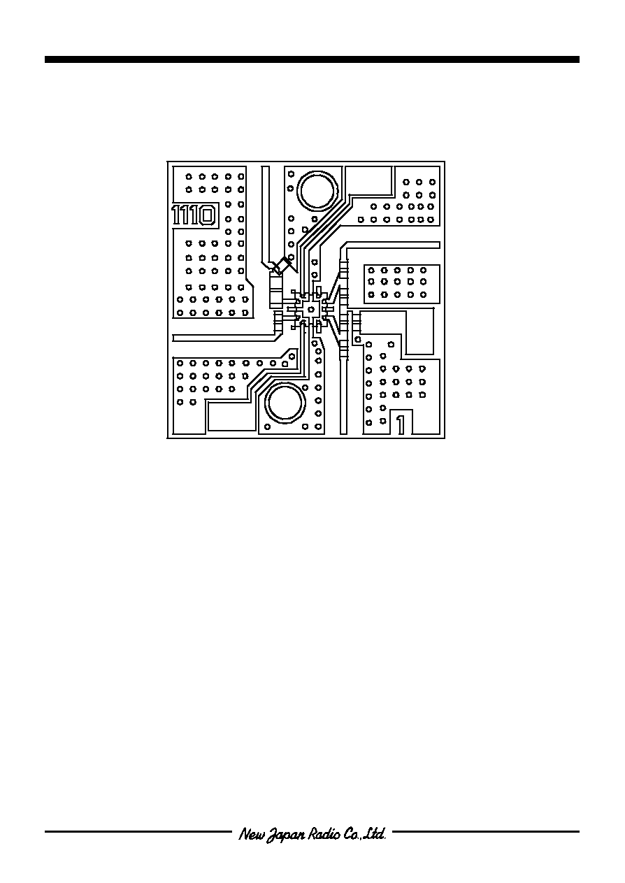
RECOMMENDED PCB DESIGN
PRECAUTIONS
[1] Please locate L2, L4, L3, and L5 close to IC.
[2] Please locate C3 close to L3, L5.
[3] Please layout each parts as close as possible.
PCB (FR-4): t=0.2mm
MICROSTRIP LINE WIDTH=0.4mm (Z
0
=50
)
PCB SIZE=17x17mm
1500MHz Band
RF OUTPUT 2
800MHz Band
RF INPUT 1
800MHz Band
RF OUTPUT 1
1500MHz Band
RF INPUT 2
VCTL
VINV
VDD
L1
L3
L4
C1
L5
C2
C3
L2
(Top View)
NJG1110PB1
- 17 -
n
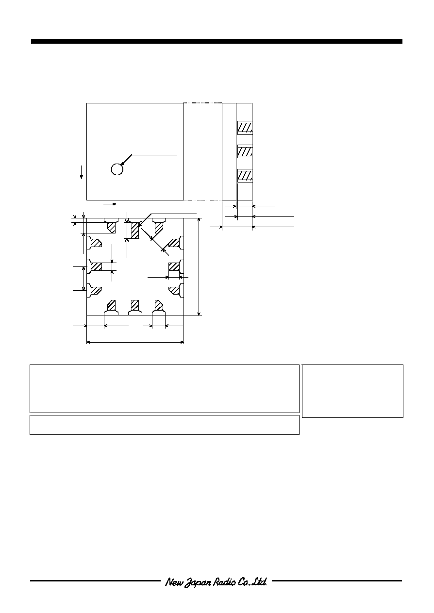
PACKAGE OUTLINE (FFP12-B1)
0.85±0.15
0
.
1
0
3
0
.
3
0
3
0
.
5
0
0.365
0.27
2
.
0
±
0
.
1
0
.
3
0
0.20
2pin INDEX
1pin INDEX
0
.
1
7
0.254±0.1
0.35
(TOP VIEW)
(BOTTOM VIEW)
(SIDE VIEW)
1
2
p
i
n
1pin
2.0±0.1
0.3
5
Cautions on using this product
This product contains Gallium-Arsenide (GaAs) which is a harmful material.
∑
Do NOT eat or put into mouth.
∑
Do NOT dispose in fire or break up this product.
∑
Do NOT chemically make gas or powder with this product.
∑
To waste this product, please obey the relating law of your country.
This product may be damaged with electric static discharge (ESD) or spike voltage. Please handle
with care to avoid these damages.
[CAUTION]
The specifications on this databook are only
given for information , without any guarantee
as regards either mistakes or omissions. The
application circuits in this databook are
described only to show representative usages
of the product and not intended for the
guarantee or permission of any right including
the industrial rights.
UNIT
: mm
PCB
: Ceramic
OVER COAT
: Epoxy resin
TERMINAL TREAT : Au
WEIGHT
: 10mg