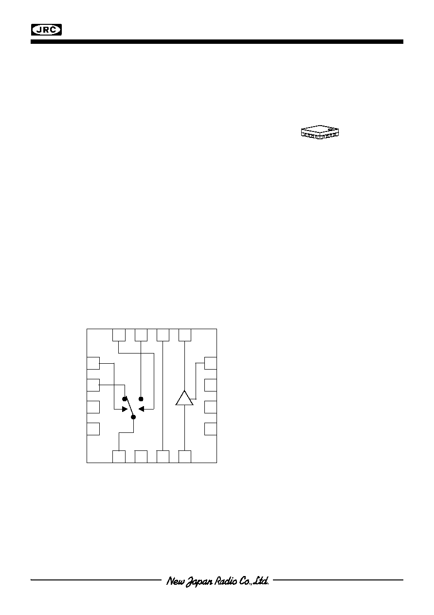
NJG1312PC1
- 1 -
SPDT SWITCH DRIVER AMPLIFIRE GaAs MMIC
n
GENERAL DESCRIPTION
n
PACKAGE OUTLINE
NJG1312PC1 is a GaAs MMIC mainly designed for CDMA
800MHz band cellular phone handsets.
This Ic features low current consumption and variable gain.
An ultra small & thin FFP package is adopted.
n
FEATURES
l
Low supply voltage operation
+2.9V typ.
l
Low current consumption
17mA typ. @ P
out
=+5.6dBm
l
High gain
19dB typ. @ 900MHz
l
Pout at 1dB Gain Compression point
+10dBm typ. @ 900MHz
l
Ultra small & thin package
FFP16-C1 (Mount Size: 2.5x2.5x0.85mm)
n
PIN CONFIGURATION
NJG1312PC1
Pin Connection
1.PC
9.RF
out
2.GND 10.GND
3.GND 11.P2
4.RF
in
12. V
CTR2
5.NC
13. V
CTR1
6.GND 14.P1
7.GND 15.GND
8.BPC 16.GND
FFP16 Type
(Top View)
1
2
16
14
15
13
3
4
5
6
7
8
9
10
11
12

NJG1312PC1
- 2 -
n
ABSOLUTE MAXIMUM RATINGS
(T
a
=+25�C, Z
s
=Z
l
=50
)
PARAMETER
SYMBOL
CONDITIONS
RATINGS
UNITS
Drain Voltage
V
DD
6
V
Control Voltage
V
CTL
6
V
Input Power
P
in
V
DD
=2.9V
15
dBm
Power Dissipation
P
D
400
mW
Operating Temperature
T
opr
-40~+85
�C
Storage Temperature
T
stg
-55~+125
�C
n
ELECTRICAL CHARACTERISTICS
(V
DD
=2.9V, V
CTR
=2.7V, f=900MHz, T
a
=-20~+80�C, Z
s
=Z
l
=50
, R
s
(External)=180
)
PARAMETER
SYMBOL
CONDITIONS
MIN
TYP
MAX
UNITS
Operating Frequency
Freq
887
900
925
MHz
Drain Voltage
V
DD
2.7
2.9
5.0
V
Operating Current
I
DD
RF SW ON
P
out
=+5.6dBm
-
17
22
mA
Control Current
I
CTL
-
1.0
2.0
uA
Control Voltage(LOW)
V
CTL
(L)
-0.2
0
0.2
V
Control Voltage(HIGH)
V
CTL
(H)
2.5
2.7
5.5
V
Small Signal Gain
Gain
RF SW ON
P
in
=-15dBm
17
19
22
dB
Gain Flatness
G
flat
RF SW ON
P
in
=-15dBm
f=887~925MHz
-
0.5
-
dB
Gain Control Range
G
cont
P
in
=-15dBm
-28.5
-27
-25.5
dB
Pout at 1dB Gain
Compression point
P
-1dB
RF SW ON
-
+10
-
dBm
IN-Band Spurious1
IBS1
RF SW ON,
P
out
=+5.6dBm
OFFSET 900kHz
-
-55
-51
dBc
IN-Band Spurious2
IBS2
RF SW ON,
P
out
=+5.6dBm
OFFSET 1.98MHz
-
-73
-68
dBc
Input VSWR
VSWR
i
RF SW ON
-
2.4
3.0
Output VSWR
VSWR
o
RF SW ON
-
1.4
2.0
Note)
RF SW ON/OFF in the table above: Control voltages (V
CTL1
, V
CTL2
) are as follows
RF SW ON
P1: V
CTL1
=0V,
V
CTL2
=2.7V
P2: V
CTL1
=2.7V, V
CTL2
=0V
RF SW OFF
P1: V
CTL1
=2.7V, V
CTL2
=0V
P2: V
CTL1
=0V,
V
CTL2
=2.7V
NJG1312PC1
- 3 -
n
TERMINAL INFORMATION
No.
SYMBOL
DESCRIPTIONS
1
PC
RF output terminal of SW.
2
GND
Ground terminal.
3
GND
Ground terminal.
4
RF
in
RF signal input terminal of driver amplifier.
5
NC
Neutral terminal. Should be connected to the ground.
6
GND
Ground terminal.
7
GND
Ground terminal.
8
BPC
Source electrode terminal of driver amplifier.
The operating current is chosen by a resistor connected
between this terminal and ground.
9
RF
out
RF signal output terminal of driver amplifier.
Please use choke coil for power supply of driver amplifier at
this terminal.
10
GND
Ground terminal.
11
P2
RF input terminal 2 of SW.
12
V
CTL2
Control terminal 2 of RF signal. Please see the truth table.
13
V
CTL1
Control terminal 1 of RF signal. Please see the truth table.
14
P1
RF input terminal 1 of SW.
15
GND
Ground terminal.
16
GND
Ground terminal.
Notice: PC terminal at pin 1 should be connected to the GND
through high resistance for pull-down (Max 560K
).
n
TRUTH TABLE
V
CTL1
V
CTL2
P1-PC
P2-PC
0V
2.7V
ON
OFF
2.7V
0V
OFF
ON
NJG1312PC1
- 4 -
n
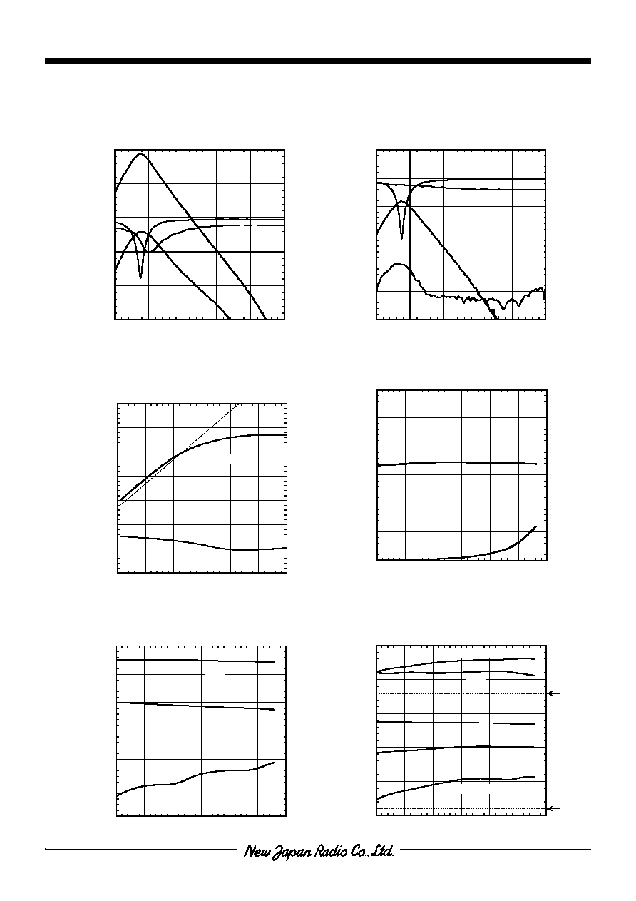
TYPICAL CHARACTERISTICS
-50
-40
-30
-20
-10
0
10
-70
-60
-50
-40
-30
-20
-10
0.5
1
1.5
2
2.5
3
S11,S21,S22 (dB)
S12 (dB)
Frequency (GHz)
S21
S22
S11
S12
(V
DD
=2.9V, V
CTR
=2.7V, RF SW OFF)
FREQUENCY CHARACTERISTIC
-30
-20
-10
0
10
20
-50
-40
-30
-20
-10
0
0.5
1
1.5
2
2.5
3
S11,S21,S22 (dB)
S12 (dB)
Frequency (GHz)
S21
S22
S11
S12
(V
DD
=2.9V, V
CTR
=2.7V, RF SW ON)
FREQUENCY CHARACTERISTIC
-15
-10
-5
0
5
10
15
20
10
15
20
25
30
35
40
45
-20
-15
-10
-5
0
5
10
Pout (dBm)
I
DD
(mA)
Pin (dBm)
Pout
I
DD
P-1dB 9.73dBm
Pin vs. Pout, I
DD
(V
DD
=2.9V, V
CTR
=2.7V, f=900MHz)
0
5
10
15
20
25
30
0
0.1
0.2
0.3
0.4
0.5
0.6
-50
-25
0
25
50
75
100
Gain, G
cont
(dB)
G
flat
(dB)
Ambient Temperature (
o
C)
Gain, G
cont
, G
flat
vs. TEMPERATURE
(V
DD
=2.9V, V
CTR
=2.7V, f=900MHz)
G
flat
Gain
G
cont
0
5
10
15
20
25
50
55
60
65
70
75
-50
-25
0
25
50
75
100
P-1dB, Psat, OIP3 (dBm)
In Band Spurios (dBc) Pout =5.6dBm
Ambient Temperature (
o
C)
Psat
P-1dB
1.98MHz offset
0.9MHz offset
P-1dB, Psat, IN BAND SPURIOUS
vs. TEMPERATURE
(V
DD
=2.9V, V
CTR
=2.7V, f=900MHz)
OIP3
0
5
10
15
20
25
30
0
1
2
3
4
5
6
-50
-25
0
25
50
75
100
I
CTR
(uA)
(V
DD
=2.9V, V
CTR
=2.7V, f=900MHz, P
out
=5.6dBm)
I
DD
, I
CTR
vs. TEMPERATURE
I
DD
(mA)
I
DD
I
CTR
FREQUENCY CHARACTERISTICS
FREQUENCY CHARACTERISTICS

NJG1312PC1
- 5 -
n
TYPICAL CHARACTERISTICS
Driver Amp. Scattering Parameters Table (V
DD
=2.9V, R
s
=180
, Z
o
=50
)
Freq.
S 11
S 21
S 12
S 22
mag
ang
mag
ang
mag
ang
mag
ang
(GHz)
(U)
(deg)
(U)
(deg)
(U)
(deg)
(U)
(deg)
0.50
0.902
-20.1
4.427
-177.6
0.036
53.9
0.763
-47.8
0.60
0.907
-25.8
4.762
172.6
0.040
49.6
0.757
-56.9
0.70
0.901
-31.2
4.897
164.1
0.044
45.4
0.699
-63.4
0.80
0.896
-36.8
5.018
155.4
0.048
41.9
0.701
-70.6
0.90
0.880
-41.9
4.992
147.8
0.051
37.6
0.667
-77.0
1.00
0.864
-46.9
5.006
140.2
0.053
35.0
0.660
-83.2
1.10
0.839
-52.0
4.891
133.3
0.055
32.6
0.651
-88.6
1.20
0.824
-56.6
4.837
126.4
0.058
28.1
0.636
-94.7
1.30
0.797
-61.1
4.675
120.3
0.061
27.1
0.642
-99.9
1.40
0.779
-65.6
4.580
113.7
0.061
22.8
0.636
-105.8
1.50
0.754
-69.6
4.428
108.0
0.063
21.4
0.640
-110.2
1.60
0.737
-73.8
4.301
102.0
0.064
19.0
0.640
-115.1
1.70
0.715
-77.4
4.122
96.9
0.064
15.3
0.640
-119.4
1.80
0.696
-81.3
3.973
91.6
0.067
13.3
0.643
-123.5
1.90
0.676
-84.5
3.800
86.3
0.066
10.4
0.644
-127.8
2.00
0.663
-88.0
3.653
81.2
0.067
7.8
0.648
-131.7
2.10
0.644
-90.8
3.478
76.5
0.068
6.2
0.651
-135.3
2.20
0.628
-93.9
3.334
71.9
0.068
3.9
0.659
-139.5
2.30
0.617
-96.3
3.163
67.3
0.069
1.7
0.662
-143.0
2.40
0.603
-98.9
3.016
62.7
0.069
-1.3
0.676
-147.1
2.50
0.594
-101.0
2.850
58.3
0.069
-3.5
0.683
-150.9
2.60
0.582
-102.9
2.702
54.1
0.070
-6.6
0.697
-154.6
2.70
0.577
-104.6
2.546
50.0
0.070
-10.5
0.706
-158.4
2.80
0.574
-106.1
2.389
46.3
0.069
-13.1
0.722
-161.9
2.90
0.577
-107.3
2.234
42.6
0.069
-17.0
0.733
-165.5
3.00
0.580
-108.4
2.069
39.6
0.066
-21.0
0.747
-168.9
NJG1312PC1
( TOP VIEW )
8
6
9
7
10
5
11
12
13
14
15
16
1
2
3
4
Rs
180
S22
S11
Ref.
Ref.
Driver Amp. Scattering Parameters