NJG1528HD3
- 1 -
DPDT SWITCH GaAs MMIC
n
GENERAL DESCRIPTION
n
PACKAGE OUTLINE
NJG1528HD3 is a GaAs high power DPDT switch
MMIC for antenna switch of tri- and dual-mode cellular
phone application such as CDMA, AMPS and PCS.
This switch features low loss, high isolation at high
power.
The ultra small & ultra thin USB6-D3 package is
applied.
n
FEATURES
l
Low voltage operation
2.5V min.
l
Pin at 0.2dB compression point
36dBm typ. @f=1.9GHz, V
CTL
=2.8V
l
Low insertion loss
0.60dB typ. @f=0.9GHz, P
IN
=31dBm, V
CTL
=2.8V
0.70dB typ. @f=1.9GHz, P
IN
=25dBm, V
CTL
=2.8V
l
High isolation
23dB typ. @f=0.9GHz, P
IN
=31dBm, V
CTL
=2.8V
17dB typ. @f=1.9GHz, P
IN
=25dBm,V
CTL
=2.8V
l
Low control current
10uA typ. @f=0.9GHz, P
IN
=31dBm, V
CTL
=2.8V
l
Ultra small & ultra thin package
USB6-D3 (Package size: 2.0x1.8x0.8mm)
n
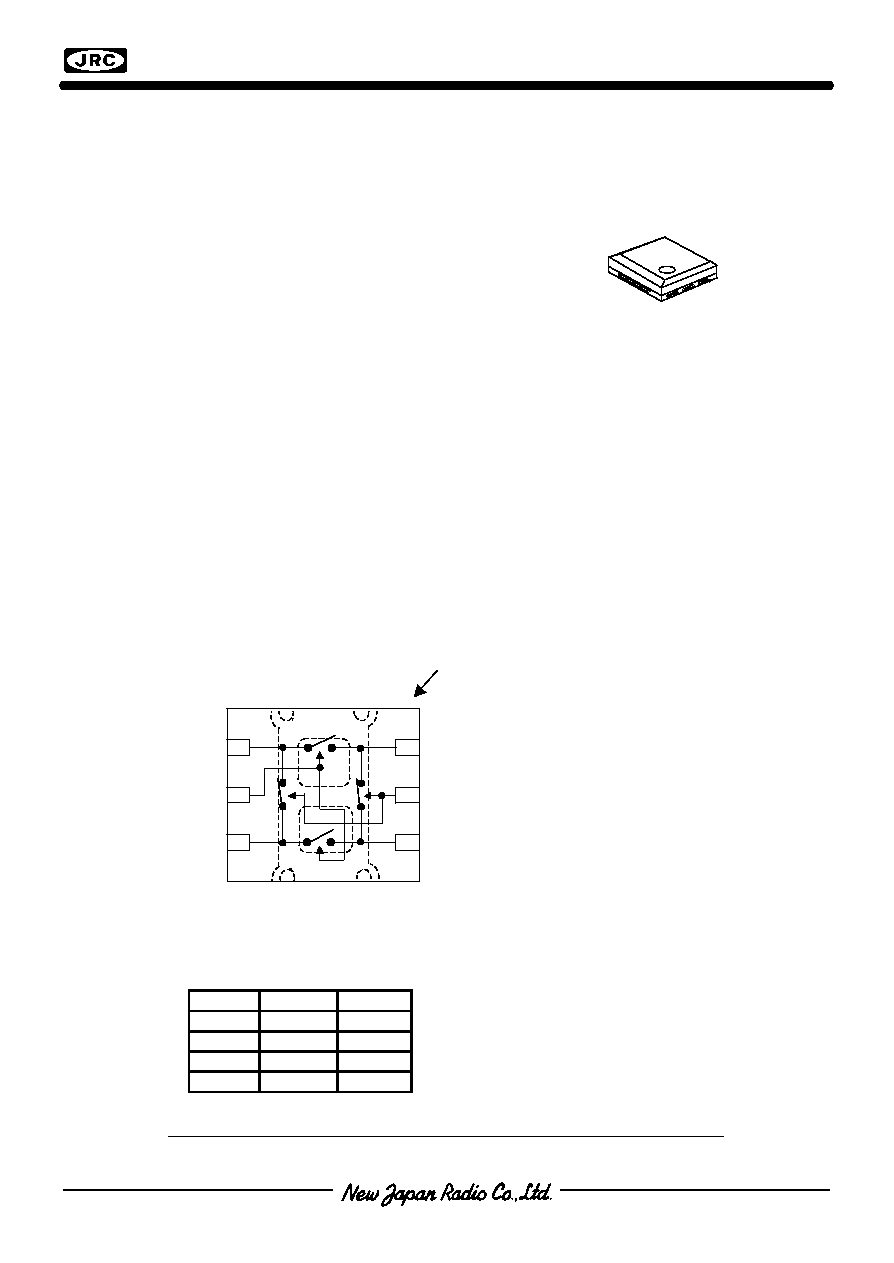
PIN CONFIGURATION
n
TRUTH TABLE
NOTE: Please note that any information on this catalog is subject to change.
NJG1528HD3
Pin connection
1. P1
2. VCTL1
3. P2
4. P3
5. VTL2
6. P4
Orientation Mark
ON Pass VCTL1
VCTL2
P1-P2
L
H
P3-P4
L
H
P1-P4
H
L
P2-P3
H
L
1
2
3
6
5
4
USB6-D3 Type
(TOP VIEW)

NJG1528HD3
- 2 -
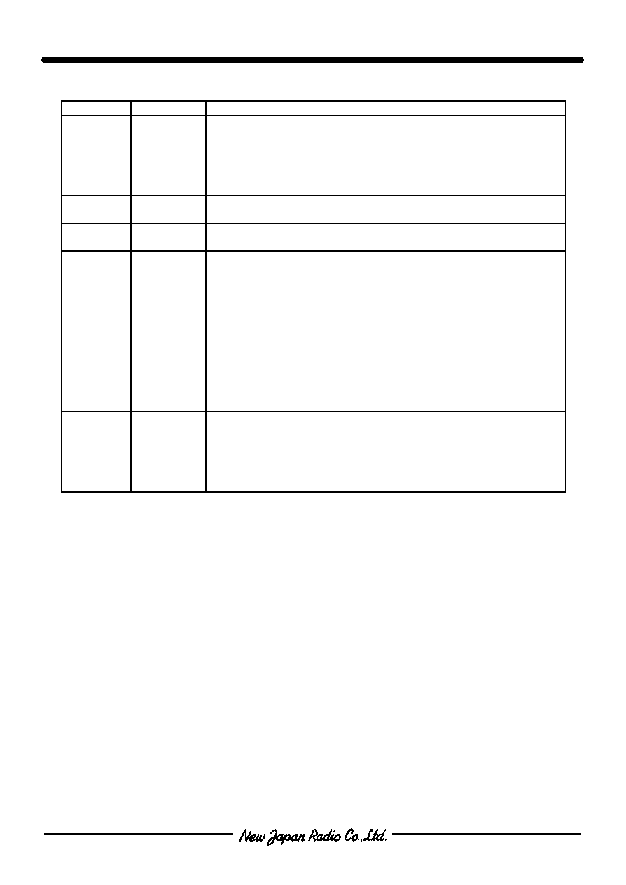
n
ABSOLUTE MAXIMUM RATINGS
(T
a
=+25�C, Z
s
=Z
l
=50
)
PARAMETER
SYMBOL
CONDITIONS
RATINGS
UNITS
RF Input Power
P
IN
V
CTL(L)
=0V, V
CTL(H)
=3V
37.5
dBm
Operating Voltage
V
CTL
V
CTL(H)
-V
CTL(L)
12
V
Power Dissipation
P
D
200
mW
Operating Temp.
T
opr
-40~+85
�C
Storage Tempe.
T
stg
-55~+150
�C
n
ELECTRICAL CHARACTERISTICS
(General conditions: T
a
=+25�C, Z
s
=Z
l
=50
, V
CTL (L)
=0V, V
CTL (H)
=2.8V)
PARAMETER
SYMBOL
CONDITIONS
MIN
TYP
MAX
UNITS
Control Voltage (Low)
V
CTL (L)
f=0.01~2.5GHz
-0.2
0
0.2
V
Control Voltage (High)
V
CTL (H)
f=0.01~2.5GHz
2.5
2.8
6.5
V
Control Current
I
CTL
f=0.9GHz, P
IN
=31dBm
-
10
20
uA
Insertion loss 1
LOSS1 f=0.9GHz, P
IN
=31dBm
-
0.60
0.75
dB
Insertion loss 2
LOSS2 f=1.9GHz, P
IN
=25dBm
-
0.75
0.90
dB
Isolation 1
(P1-P2, P3-P4, P1-P4
P2-P3, P1-P3, P2-P4)
ISL1
f=0.9GHz, P
IN
=31dBm
21
23
-
dB
Isolation 2
(P1-P2, P3-P4, P1-P4
P2-P3, P1-P3, P2-P4)
ISL2
f=0.9GHz, P
IN
=31dBm
16
17
-
dB
Pin at 0.2dB
Compression point
P
-0.2dB
f=1.9GHz
33.5
36
-
dBm
2nd Harmonics 1
2fo(1)
f=0.9GHz, P
IN
=25dBm
-
-
-70
dBc
2nd Harmonics 2
2fo(2)
f=1.9GHz, P
IN
=25dBm
-
-
-65
dBc
3rd Harmonics 1
3fo(1)
f=0.9GHz, P
IN
=25dBm
-
-
-65
dBc
3rd Harmonics 2
3fo(2)
f=1.9GHz, P
IN
=25dBm
-
-
-65
dBc
Input 3
rd order
intercept Point 1
IIP3(1)
f=900+901MHz,
Pin=25dBm *1
-
60
-
dBm
Input 3
rd order
intercept Point 2
IIP3(2)
f=1900+1901MHz,
Pin=25dBm *1
-
60
-
dBm
VSWR
VSWR
i
on-state ports, f=1.9GHz
-
1.2
1.4
Switching time
T
SW
f=0.1~2.5GHz
-
100
-
ns
*1: The input IP3 is defined as following equation.
IIP3=(3 x Pout - IM3) / 2 + LOSS
NJG1528HD3
- 3 -
n
TERMINAL INFORMATION
No.
SYMBOL
EXPLANATION
1
P1
RF port. This port is connected with P2 port by controlling
2pin-V
CTL(H)
(+2.5~+6.5V) and 5pin-V
CTL(L)
(-0.2~+0.2V).
This port is connected with P4 port by controlling 2pin-V
CTL(L)
(-0.2~+0.2V) and 5pin-V
CTL(H)
(+2.5~+6.5V).
A DC cut capacitor 56pF is reguired at this terminal to block DC
voltage of inner circuit.
2
VCTL1
Control port1. Please connect bypass capacitor (10pF) between this
terminal and GND close to this IC.
3
VCTL2
Control port2. Please connect bypass capacitor (10pF) between this
terminal and GND close to this IC.
4
P2
RF port. This port is connected with P1 port by controlling
2pin-V
CTL(L)
(-0.2~+0.2V) and 5pin-V
CTL(H)
(+2.5~+6.5V).
This port is connected with P3 port by controlling 2pin-V
CTL(H)
(+2.5~+6.5V) and 5pin-V
CTL(L)
(-0.2~+0.2V).
A DC cut capacitor 56pF is reguired at this terminal to block DC
voltage of inner circuit.
5
P3
RF port. This port is connected with P2 port by controlling
2pin-V
CTL(H)
(+2.5~+6.5V) and 5pin-V
CTL(L)
(-0.2~+0.2V).
This port is connected with P4 port by controlling 2pin-V
CTL(L)
(-0.2~+0.2V) and 5pin-V
CTL(H)
(+2.5~+6.5V).
A DC cut capacitor 56pF is reguired at this terminal to block DC
voltage of inner circuit.
6
P4
RF port. This port is connected with P1 port by controlling
2pin-V
CTL(H)
(+2.5~+6.5V) and 5pin-V
CTL(L)
(-0.2~+0.2V).
This port is connected with P3 port by controlling 2pin-V
CTL(L)
(-0.2~+0.2V) and 5pin-V
CTL(H)
(+2.5~+6.5V).
A DC cut capacitor 56pF is reguired at this terminal to block DC
voltage of inner circuit.
NJG1528HD3
- 4 -
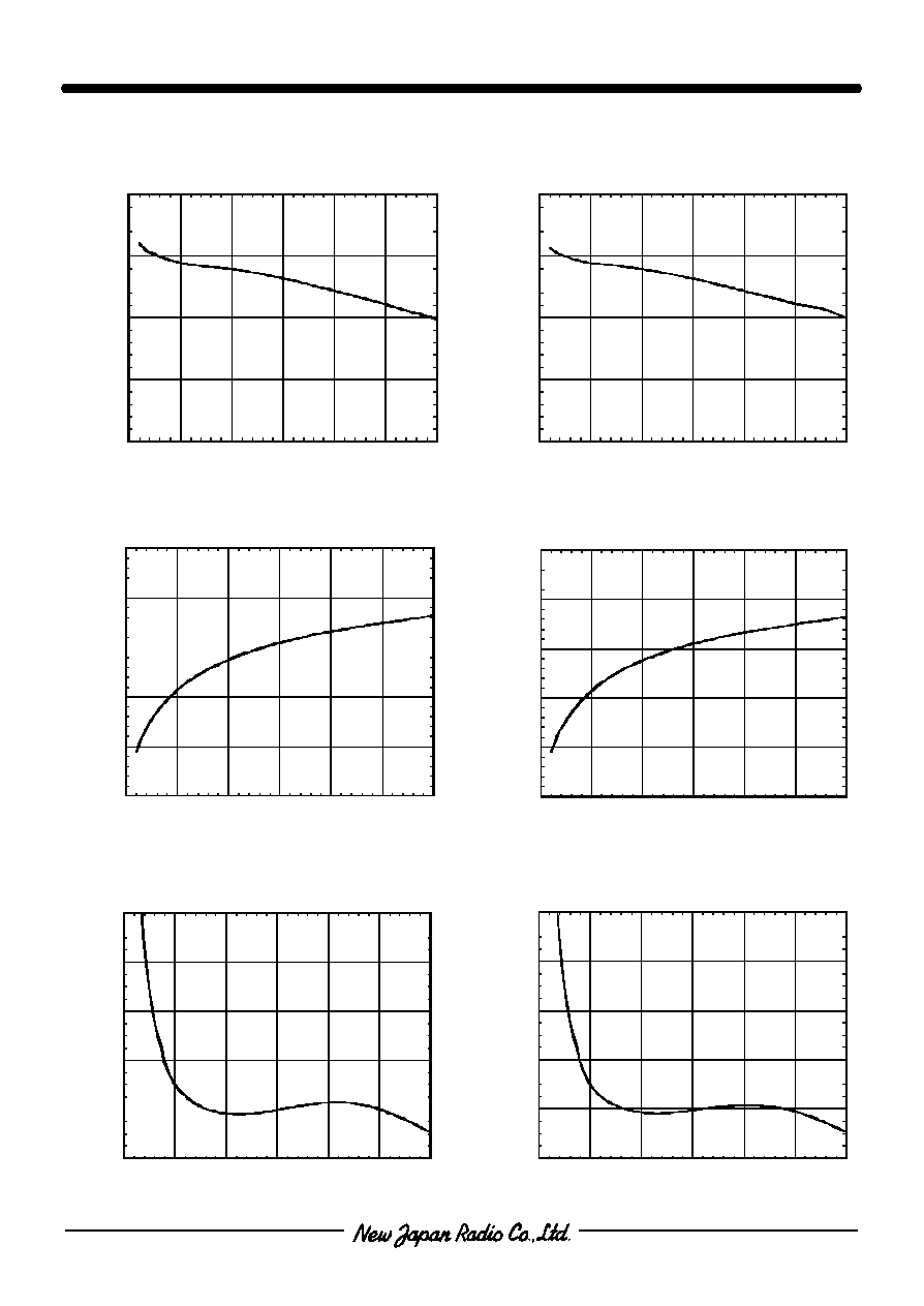
n
ELECTRICAL CHARACTERISTICS
(with application circuit, losses of PCB, connector and DC blocking capacitor are excluded)
-2.0
-1.5
-1.0
-0.5
0.0
0.0
0.5
1.0
1.5
2.0
2.5
3.0
(P1-P2/P3-P4 ON, VCTL=0V/2.8V, Pin=-10dBm)
Insertion Loss (dB)
Frequency (GHz)
P1-P2 Insertion Loss vs. Frequency
-50
-40
-30
-20
-10
0
0.0
0.5
1.0
1.5
2.0
2.5
3.0
(P1-P4/P3-P2 ON, VCTL=0V/2.8V, Pin=-10dBm)
Isolation (dB)
Frequency (GHz)
P1-P2 Isolation vs. Frequency
1.0
1.2
1.4
1.6
1.8
2.0
0.0
0.5
1.0
1.5
2.0
2.5
3.0
(P1-P2/P3-P4 ON, VCTL=0V/2.8V, Pin=-10dBm)
VSWR
Frequency (GHz)
P1-P2 VSWR vs. Frequency
-2.0
-1.5
-1.0
-0.5
0.0
0.0
0.5
1.0
1.5
2.0
2.5
3.0
(P1-P2/P3-P4 ON, VCTL=0V/2.8V, Pin=-10dBm)
Insertion Loss (dB)
Frequency (GHz)
P3-P4 Insertion Loss vs. Frequency
-50
-40
-30
-20
-10
0
0.0
0.5
1.0
1.5
2.0
2.5
3.0
(P1-P4/P3-P2 ON, VCTL=0V/2.8V, Pin=-10dBm)
Isolation (dB)
Frequency (GHz)
P3-P4 Isolation vs. Frequency
1.0
1.2
1.4
1.6
1.8
2.0
0.0
0.5
1.0
1.5
2.0
2.5
3.0
(P1-P2/P3-P4 ON, VCTL=0V/2.8V, Pin=-10dBm)
VSWR
Frequency (GHz)
P3-P4 VSWR vs. Frequency
NJG1528HD3
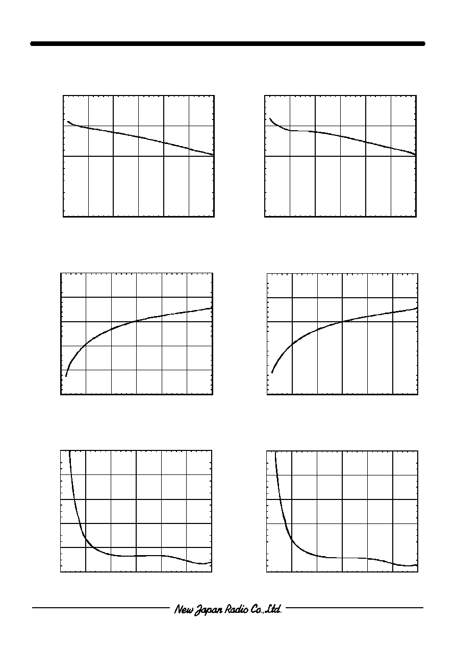
- 5 -
n
ELECTRICAL CHARACTERISTICS
(with application circuit, losses of PCB, connector and DC blocking capacitor are excluded)
-2.0
-1.5
-1.0
-0.5
0.0
0.0
0.5
1.0
1.5
2.0
2.5
3.0
(P1-P4/P3-P2 ON, VCTL=0V/2.8V, Pin=-10dBm)
Insertion Loss (dB)
Frequency (GHz)
P1-P4 Insertion Loss vs. Frequency
-50
-40
-30
-20
-10
0
0.0
0.5
1.0
1.5
2.0
2.5
3.0
(P1-P2/P3-P4 ON, VCTL=0V/2.8V, Pin=-10dBm)
Isolation (dB)
Frequency (GHz)
P1-P4 Isolation vs. Frequency
1.0
1.2
1.4
1.6
1.8
2.0
0.0
0.5
1.0
1.5
2.0
2.5
3.0
(P1-P4/P3-P2 ON, VCTL=0V/2.8V, Pin=-10dBm)
VSWR
Frequency (GHz)
P1-P4 VSWR vs. Frequency
-2.0
-1.5
-1.0
-0.5
0.0
0.0
0.5
1.0
1.5
2.0
2.5
3.0
(P1-P4/P3-P2 ON, VCTL=0V/2.8V, Pin=-10dBm)
Insertion Loss (dB)
Frequency (GHz)
P3-P2 Insertion Loss vs. Frequency
-50
-40
-30
-20
-10
0
0.0
0.5
1.0
1.5
2.0
2.5
3.0
(P1-P2/P3-P4 ON, VCTL=0V/2.8V, Pin=-10dBm)
Isolation (dB)
Frequency (GHz)
P3-P2 Isolation vs. Frequency
1.0
1.2
1.4
1.6
1.8
2.0
0.0
0.5
1.0
1.5
2.0
2.5
3.0
(P1-P4/P3-P2 ON, VCTL=0V/2.8V, Pin=-10dBm)
VSWR
Frequency (GHz)
P3-P2 VSWR vs. Frequency