 | –≠–ª–µ–∫—Ç—Ä–æ–Ω–Ω—ã–π –∫–æ–º–ø–æ–Ω–µ–Ω—Ç: NJL6165R | –°–∫–∞—á–∞—Ç—å:  PDF PDF  ZIP ZIP |
NJL6165R/6165R-1
- 1 -
NJL6165R
1.
3
5
1.
3
5
1.0
(2x)R0.3
2.5
1.16
0.5
1.0
0.3
0.
7
0.
3
4.
9
2.
5
NJL6165R-1
0.5
1.16
1.
8
3.
6
1.8
1.0
0.3
0.
3
0.
3
0.
9
5
0.
9
5
1.0
(2x)R0.3
HIGH SPEED PIN PHOTO DIODE
s
GENERAL DESCRIPTION
s
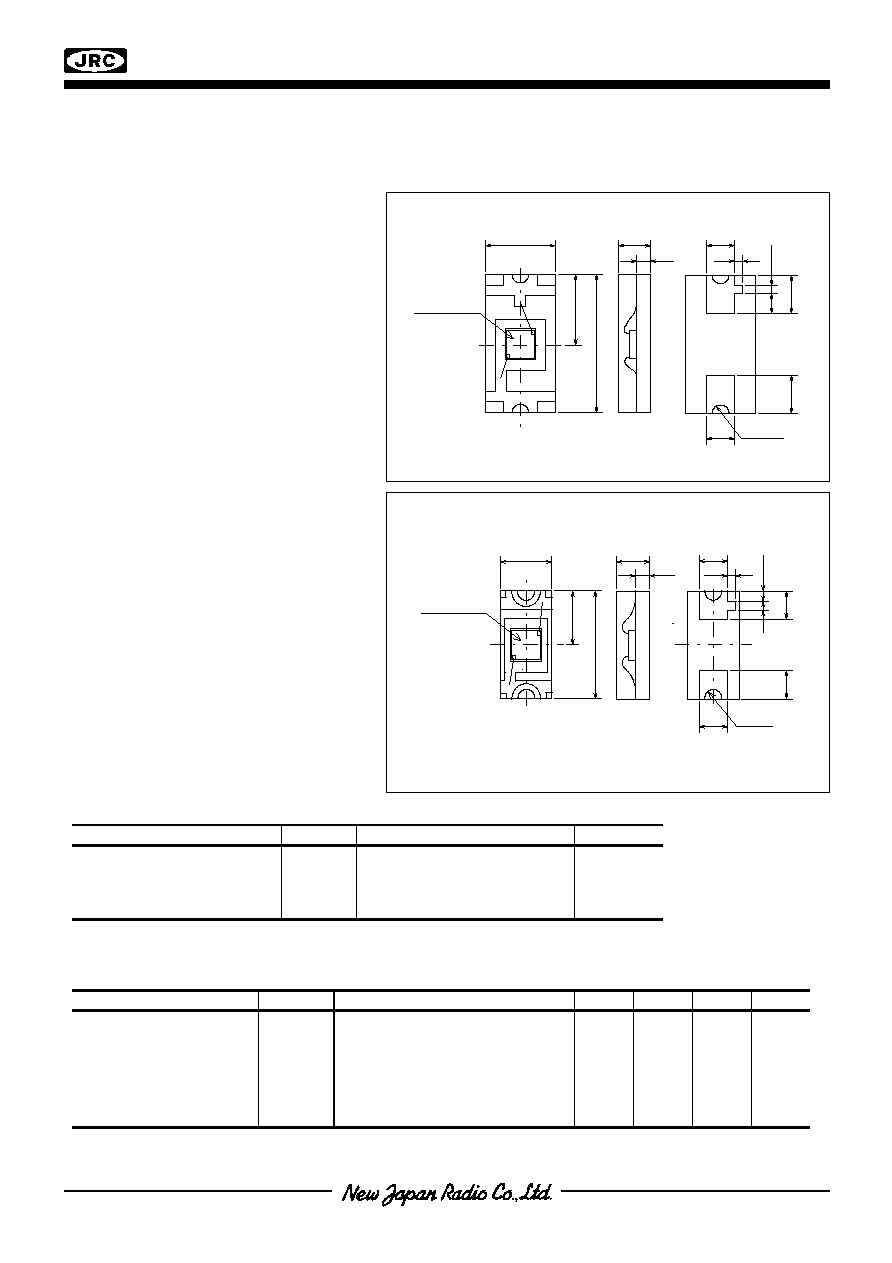
OUTLINE (typ.)
Unit : mm
The NJL6165R/6165R-1 are the PIN photo
diode, which attain high speed (fc : 300MHz)
and high sensitivity (S : 0.65A/W).
It shrinks the outline by COBP(Chip on Board
Package), and attain under half package
volume compared with lead frame type.
s
FEATURES
∑ High speed, high sensitivity
∑ Super miniature, super thin type
NJL6165R (2.5mmX4.9mmX1.16mm)
NJL6165R-1 (1.8mmX3.6mmX1.16mm)
s
APPLICATIONS
∑ Laser monitor for CD-R/RW etc.
∑ Reading the signal for optical communication
etc.
s
ABSOLUTE MAXIMUM RATINGS
(Ta=25
∞
C)
PARAMETER SYMBOL
RATINGS
UNIT
Reverse Voltage
Operating Temperature
Storage Temperature
Reflow Soldering Temperature
V
R
T
opr
T
stg
T
sol
35
-30 to +85
-40 to +100
260 (10sec.)
V
∞
C
∞
C
∞
C
s
ELECTRO-OPTICAL CHARACTERISTICS
(Ta=25
∞
C)
PARAMETER SYMBOL
TEST
CONDITION
MIN
TYP
MAX
UNIT
Dark Current
Forward Voltage
Capacitance
Peak Wavelength
Sensitivity
Cut off Frequency
I
D
V
F
C
t
P
S
fc
V
R
=10V
I
F
=1mA
V
R
=2.0V, f=1MHz
--
V
R
=2.0V,
=780nm (note)
V
R
=2.0V,
=780nm, RL=50
,
-3dB
--
--
--
--
0.50
--
0.1
--
4
800
0.65
300
2.0
1.0
--
--
--
--
nA
V
pF
nm
A/W
MHz
(note) in the case of illuminating all over the package
anode
cathode
anode
cathode
Active area: 0.7mm square
Active area
Active area: 0.7mm square
Active area
NJL6165R/6165R-1
- 2 -
0
1
2
3
4
5
0
1
2
3
4
5
Reverse Voltage
VR(V)
Ri
s
e
T
i
m
e
tr
(
n
s
)
=780nm, RL=50
0
1
2
3
4
5
0
1
2
3
4
5
Reverse Voltage
VR(V)
Fa
l
l
T
i
m
e
tr
(
n
s
)
=780nm, RL=50
1.00E-13
1.00E-12
1.00E-11
1.00E-10
1.00E-09
1.00E-08
-40
-20
0
20
40
60
80
100
Ambient Temperature Ta(
)
Da
r
k
Cu
r
r
e
n
t
I
D
(
A
)
VR=2.0V,
=780nm
s
TYPICAL CHARACTERISTICS
Relative Sensitivity vs. Illuminance (Ta=25
∞
C) Spectral Response (Ta=25
∞
C)
Dark Current vs. Temperature Relative Sensitivity vs. Temperature
Rise Time vs. Reverse Voltage (Ta=25
∞
C) Fall Time vs. Reverse Voltage (Ta=25
∞
C)
1.00E-08
1.00E-07
1.00E-06
1.00E-05
1.00E-04
1.00E-03
0.01
0.1
1
10
100
Illuminance
(mW/cm
2
)
Li
ght
C
u
r
r
e
n
t
(
)
VR=2.0V,
=780nm
0
10
20
30
40
50
60
70
80
90
100
500
600
700
800
900
1000
1100
Wavelength
(nm)
R
e
la
t
i
v
e
S
e
n
s
it
iv
it
y
(
%
)
70%
75%
80%
85%
90%
95%
100%
105%
110%
115%
120%
125%
130%
-40
-20
0
20
40
60
80
100
Ambient Temperature Ta(
)
R
e
la
t
i
v
e
S
e
n
s
it
iv
it
y
(%
)
VR=2.0V,
=780nm
NJL6165R/6165R-1
- 3 -
3.0
3.5
4.0
4.5
5.0
5.5
6.0
6.5
7.0
0
1
2
3
4
5
Reverse Voltage VR(V)
C
a
pa
s
i
t
a
n
c
e C
j
(
p
F
)
Relative Sensitivity vs. Frequency ( Ta=25
∞
C) Capacitance vs. Reverse Voltage ( Ta=25
∞
C)
s
MEASURING CIRCUIT FOR RESPONSE TIME
Input
Output
90%
10%
50
OSCILLOSCOPE
Laser
NJL6165R/
NJL6165R-1
Pulse
Generator
-6
-5
-4
-3
-2
-1
0
1
10
100
1000
Frequency f(MHz)
R
e
la
t
i
v
e
Se
n
s
it
iv
it
y
(
d
B)
VR=2.0V,
=780nm,
RL=50
NJL6165R/6165R-1
- 4 -
250
200
150
100
50
0
PRECAUTION FOR HANDLING
1. Soldering to actual circuit board
Soldering condition
- Heated condition of plastic package.
Lower than 240
∞
C of maximum surface temperature, less than 30 seconds of time kept higher than 200
∞
C.
Soldering Method
1) Reflow Method
Recommended temperature profile of its method.
Preparatory heating condition
: 120 to 150
∞
C about 60 sec.
Recommended soldering temperature : 230 to 240
∞
C about 3 to 5 sec.
Slowly cool down right after soldering.
Soldering to be done within twice under this condition.
(
∞
C) 3 to 5 sec.
240
∞
C max.
Preparatory heating Less than
60 to 120 sec. 30 sec.
Time
2) Reflow Method
(
In case of infrared heating
)
- Temperature profile : Same to the above
- Avoid direct irradiation to the plastic package because it is mold resin, absorbs the Infrared Radiation and its surface
temperature will be higher than lead itself.
3) The other method
Avoid rapid heating up like dipping the devices directly into the melting solder or vapor phase method
(
VPS
).
If the device is heated to high temperature and kept in its condition for longer time, it would affect to its reliability.
It is necessary to solder in short time as soon as possible.
2. Cleaning
Avoid washing of the device after soldering by reflow method.
3. Attention in handling
1) Treat not to touch the lens surface.
2) Avoid dust and any other foreign materials (paint, bonding material, etc.) on the lens surface.
3) When mounting, special care has to be taken on the mounting position and tilting of the device because it is very
important to place the device to the optimum position to the object.
4. Storage
In order to prevent from degradation of this device in moisturing at reflow method, so that this device is contained in
dampproof packaging. So that mount the device as short as possible after opening the envelope.
NJL6165R/6165R-1
- 5 -
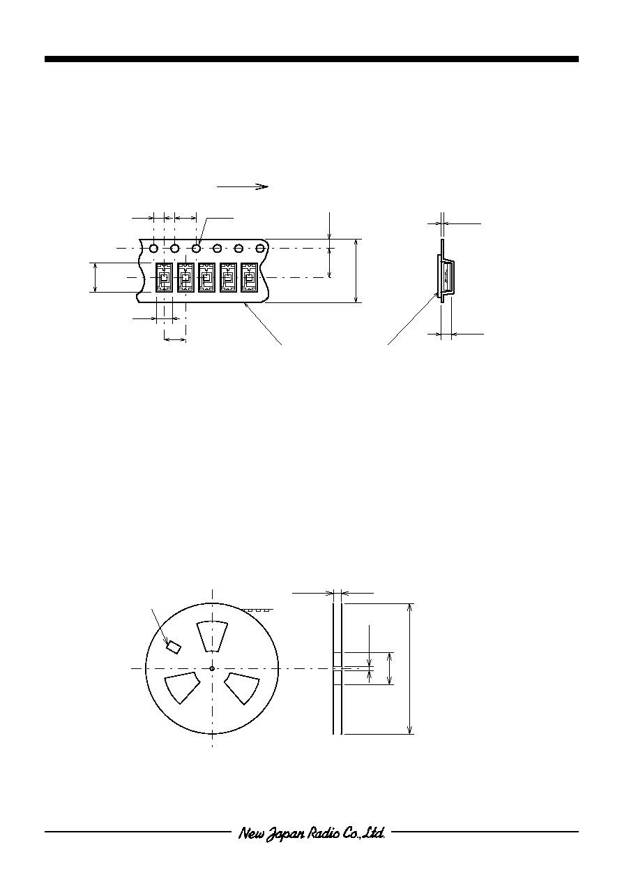
(TE1)
NJL6165R Taping Specification
1. Taping Size
1) Carrier tape is used with Styrene type Carbonated Plastic.
2) Cover tape is used with electro statistically prevention treated Polyester type tape.
3) Product taping direction is to place the index mark against the pull out direction of the tape as in the drawing.
Pull out direction of tape
2. Taping Strength
Pull up the cover tape from the carrier tape, and when the opening angle comes around 10 to 15
∞
, and the peeling-off
strength is to be within the power of 20 to 70g.
3. Packaging
1) The taped products are to be rolled up on the taping reel as on the drawing.
2) Rolling up specification
2-1) Start Rolling : Carrier tape open space more than 20 Pieces.
2-2) End of Rolling : Carrier tape open space more than 20 Pieces, and 2 round of reel space at the cover tape only.
3) Taping quantity : 2,000 Pieces
4) Seal off after putting each reels in a dampproof bag with silica gel (3 bags).
13
60
18
0
13
Label
2.0
4.0
2.9
4.0
5.
5
12
.
0
1.
75
5.
4
0.3
1.5
Carrier tape
Cover tape
1.5