NJM1431A
- 1 -
Ver.2004-01-13
ADJUSTABLE HIGH PRECISION SHUNT REGULATOR
GENERAL DESCRIPTION
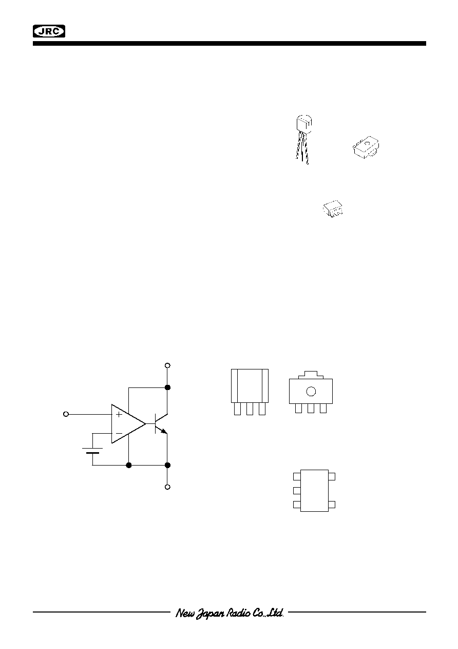
PACKAGE OUTLINE
FEATURES
Operating Voltage
V
REF
to 36V
Precision Voltage Reference
2.465V±1%
2.9mm ◊ 1.5mm to MTP (SOT23) package
Adjustable Output Voltage For
External Resistance two Parts.
Bipolar Technology
Package Outline
TO-92, SOT-89 (3pin), MTP5
BLOCK DIAGRAM
PIN CONFIGURATION
The
NJM1431A
is a precision shunt regulator.
Compared to the conventional 431, The
NJM1431A
offers
higher voltage accuracy and small package availability to
support a wide range of applications.
NJM1431AF
NJM1431AL1 NJM1431AU
ANODE
REFERENCE
V
REF
CATHODE
1. REFERENCE
2. ANODE
3. CATHODE
1
2
3
NJM1431AL1
1
2
3
NJM1431AU
CATHODE
ANODE
REFERENCE
NC
1
2
3
5
4
NC
NJM1431AF
NJM1431A
- 2 -
Ver.2004-01-13
ABSOLUTE MAXIMUM RATINGS (Ta=25∞C)
PARAMETER SYMBOL
MAXIMUM
RATINGS
UNIT
Cathode Voltage
V
KA
+37 V
Continuous Cathode Current
I
K
-100
~
150
mA
Reference Input Current
I
REF
-0.05 ~ 10
mA
Power Dissipation
P
D
(TO-92) 500
(SOT-89) 350
(MTP5) 200
mW
Operating Temperature Range
T
OPR
-40 ~ +85
∞
C
Storage Temperature Range
T
STG
-40 ~ +150
∞
C
RECOMMENDED OPERATING CONDITIONS (Ta=25∞C)
PARAMETER SYMBOL
MIN. TYP. MAX. UNIT
Cathode Voltage
V
KA
V
REF
≠ 36 V
Cathode Current
I
K
1 ≠ 100
mA
ELECTRICAL CHARACTERISTICS (I
K
=10mA, Ta=25
∞
C)
PARAMETER SYMBOL TEST
CONDITION
MIN.
TYP.
MAX.
UNIT
Reference Voltage
V
REF
V
KA
=V
REF
(*1)
2.440
2.465
2.490
V
V
REF
V
KA
10V
(*2) ≠
±
1.4
±
2.7
mV/V
Reference Voltage
Change vs. Cathode
Voltage Change
V
REF
/
V
KA
10V V
KA
36V
(*2)
≠
±
1.0
±
2.0
mV/V
Reference Input Current
I
REF
R1=10k, R2= (*2)
≠
2
4
uA
Minimum Input Current
I
MIN
V
KA
=V
REF
, V
REF
=1% (*1) ≠ 0.4 1.0
mA
Cathode Current
(Off Cond.)
I
OFF
V
KA
=36V, V
REF
=0V (*3)
≠
0.1
1.0
uA
Dynamic Impedance
Z
KA
V
KA
= V
REF
, f1kHz
1mA I
K
100mA
(*1) ≠ 0.2
0.5
TEMPERATURE CHARACTERISTICS (I
K
=10mA, Ta= -40
∞
C ~ 85
∞
C)
PARAMETER SYMBOL TEST
CONDITION
MIN.
TYP.
MAX.
UNIT
Reference Voltage
Change
V
REF
V
KA
=V
REF
(*1)
≠
8
17
mV
Reference Input Current
Change
I
REF
R1=10k, R2= (*2)
≠
0.4
1.2
uA
The maximum value of "Dynamic Impedance", "Reference Voltage Change" and "Reference Input Current Change"
are determined based on sampling evaluation from the 5 initial production lots, and thus not tested in the production test.
Therefore, these values are for the reference design purpose only.
V
REF
∑∑∑Reference voltage includes error.
(*1): Test Circuit (Fig.1)
(*2): Test Circuit (Fig.2)
(*3): Test Circuit (Fig.3)

NJM1431A
- 3 -
Ver.2004-01-13
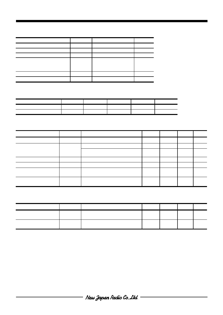
TEST CIRCUIT
Fig.1
V
KA
=V
REF
to test circuit
Fig.2 V
KA
>V
REF
to test circuit
Fig.3 I
OFF
to test circuit
V
O
=V
KA
=V
REF
1
R
I
2
R
1
R
1
V
V
V
REF
REF
KA
O
◊
+
+
=
=
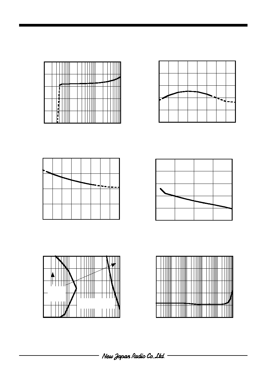
POWER DISSIPATION VS. AMBIENT TEMPERATURE
0
100
200
300
400
500
600
0
25
50
75
100
Ambient Temperature Ta (∞C)
Power Dissipat
ion
P
D
(mW)
TO-92
SOT-89
MTP5
INPUT
V
KA
I
K
V
REF
INPUT
V
KA
I
K
V
REF
I
REF
R1
R2
INPUT
V
KA
I
OFF
NJM1431A
- 4 -
Ver.2004-01-13
TYPICAL CHARACTERISTICS
2.4
2.42
2.44
2.46
2.48
2.5
0.1
1
10
100
Reference Voltage vs. Cathode Current
(V
KA
=V
REF
, Ta=25
o
C)
Cathode Current I
K
(mA)
Re
f
e
r
e
nc
e
Vo
l
t
ag
e
V
RE
F
(V
)
2.44
2.45
2.46
2.47
2.48
2.49
-50 -25
0
25
50 75 100 125 150
Ambient Temperature
Ta (
o
C)
Ref
e
r
e
nc
e
Vol
t
ag
e V
RE
F
(V
)
Reference Voltage vs. Temperature
(V
KA
=V
REF
, I
K
=10mA)
0
0.5
1
1.5
2
-50 -25
0
25
50 75 100 125 150
Ambient Temperature
Ta (
o
C)
Re
f
e
r
e
nc
e
I
n
pu
t
Cu
r
r
en
t
I
REF
(uA
)
Reference Input Current vs. Temperature
(I
K
=10mA, R1=10k
, R2= )
8
2.44
2.45
2.46
2.47
2.48
2.49
0
10
20
30
40
Reference Voltage vs. Cathode Voltage
(I
K
=10mA, R1=Variable, R2=10k
, Ta=25
o
C)
Cathode Voltage V
KA
(V)
Re
f
e
r
e
nc
e
Vo
l
t
ag
e
V
RE
F
(V
)
0
20
40
60
80
100
0.01
0.1
1
10
Aunstable Operaion
Region
Safety Operating Boundary Condition
(V
KA
=V
REF
, C
OUT
=Ceramic Capacitor, Ta=25
o
C)
Output Capacitor C
OUT
(uF)
Ca
t
hod
e
Cur
r
e
n
t
I
K
(m
A
)
Stable
Operaion
Region
0
0.1
0.2
0.3
0.4
0.5
0.001
0.01
0.1
1
10
100
Dynamic Impedance
(I
K
=1 to 100mA, V
KA
=V
REF
, Ta=25
o
C)
Cathode Current Frequency
f (kHz)
D
y
na
m
i
c
I
m
pe
da
n
c
e
|
Z
KA
| (
)
Note) Oscillation might occur while operating within the range
of safety curve.
So that, it is necessary to make ample margins by
taking considerations of fluctuation of the device.

NJM1431A
- 5 -
Ver.2004-01-13
MEMO
[CAUTION]
The specifications on this databook are only
given for information , without any guarantee
as regards either mistakes or omissions. The
application circuits in this databook are
described only to show representative usages
of the product and not intended for the
guarantee or permission of any right including
the industrial rights.