NJM2800
Low Dropout Voltage Regulator with Reset
s
GENERAL DISCRIPTION
s
PACKAGE OUTLINE
The NJM2800 is a low dropout voltage regulator with
reset function.
It provides up to 150mA of logic supply, and the reset
function monitors either input or output voltage of the
regulator with 1% accuracy.
It is suitable for local power supply and reset for small
micro controller and other logic chips.
s
FEATURES
q
Output Voltage Accuracy
Vo
=
±
1.0
%
q
Reset Voltage Accuracy
Vreset
=
±
1.0
%
q
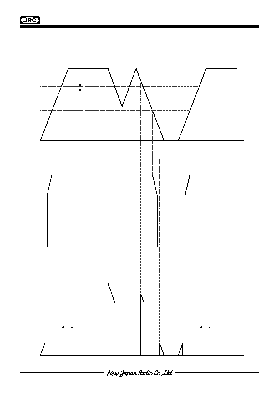
Reset Hold Time
td
=
10mS
±
1.0mS
q
Ripple Rejection
60dB typ. (f=1kHz)
q
Quiescent Current
I
Q
=
250
µ
A (typ.)
q
Input Voltage Monitor type
q
Open Collector Output
q
Internal Short Circuit Current Limit
q
Internal Thermal Overload Protection
q
Bipolar Technology
q
Package Outline
SOT89 (5pin) / MTP5
s
OUTPUT VOLTAGE/ DETECTION VOLTAGE
Device Name
Output Voltage
Detection Voltage
NJM2800F/U1803 1.8V
3.0V
NJM2800U3342 3.3V
4.2V
s
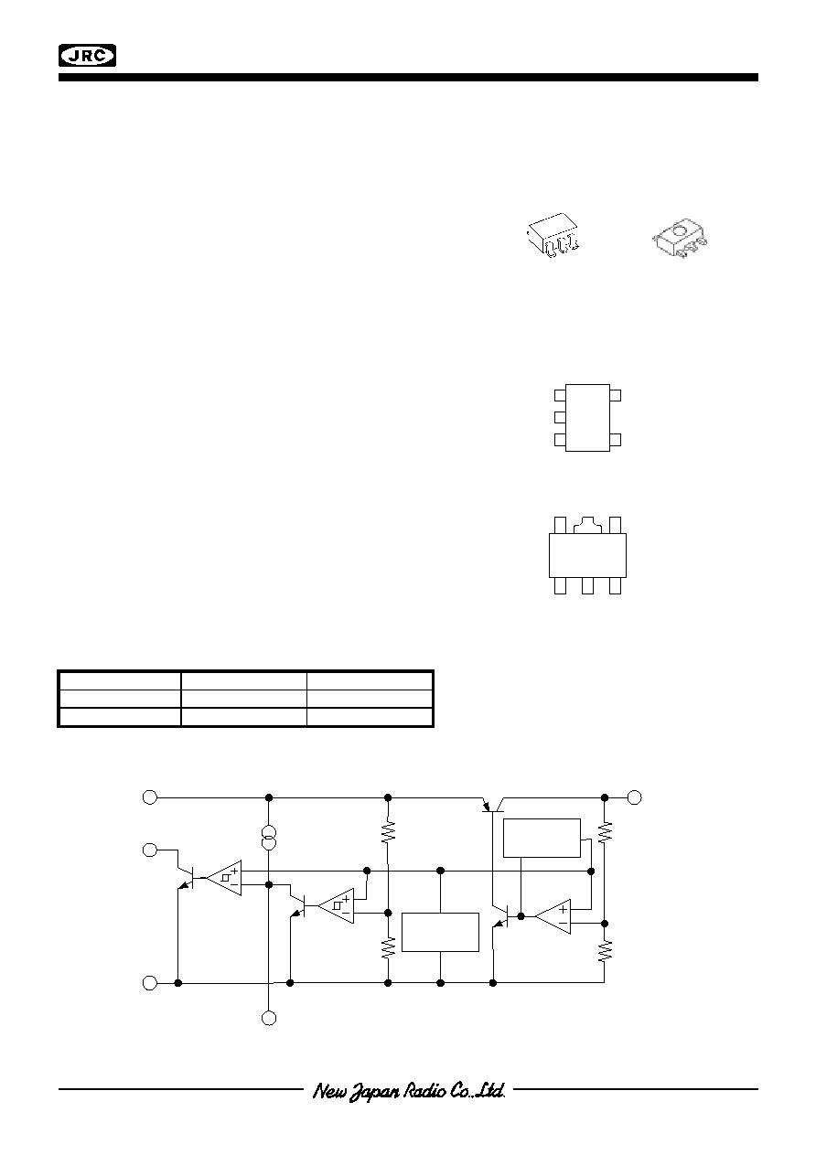
EQUIVALENT CIRCUIT
NJM2800F NJM2800U
s
PIN CONFIGURATION
1.V
OUT
2.GND
3.Cd
4.V
OR
5.V
IN
1 5
2
3 4
1.V
IN
2.GND
3.V
OR
4.C
d
5.V
OUT
5 4
1 2 3
MTP5
SOT-89(5pin)
V
O
GND
V
IN
Thermal
Protection
Bandgap
Reference
Cd
V
OR
NJM2800
s
ABSOLUTE MAXIMUM RATINGS
(Ta=25
°
C)
PARAMETER SYMBOL
RATINGS
UNIT
Input Voltage
V
IN
+14 V
200 (MTP5)
Power Dissipation
P
D
350 (SOT-89)
mW
Operating Temperature
Topr
-
40
+85
°
C
Storage Temperature
Tstg
-
40
+125
°
C
s
ELECTRICAL CHARACTERISTICS
(V
IN
=Vo+1V, C
IN
=0.1
µ
F, Co=1
µ
F
(
Vo2.6V: Co=2.2
µ
F
)
Ta=25
°
C)
PARAMETER SYMBOL
TEST
CONDITION
MIN.
TYP.
MAX.
UNIT
Quiescent Current
I
Q
V
IN
=Vo+2V, Io=0mA
-
250 350
µ
A
Regulator Block
Output Voltage
Vo
Io=30mA
-
1.0%
-
+1.0% V
Output Current
Io
Vo-0.3V
150
200
-
mA
Line Regulation
Vo/V
IN
V
IN
=Vo+1V
Vo+6V, Io=30mA
-
-
0.10 %/V
Load Regulation
Vo/Io
Io=0
100mA
-
-
0.03 %/mA
Dropout Voltage
V
I_O
Io=60mA
-
0.10 0.18 V
Ripple Rejection
RR
ein=200mVrms, f=1kHz, Io=10mA,Vo=3V
-
60
-
dB
Output Voltage Temperature
Coefficient
Vo/T
Ta=0
85
°
C, Io=10mA
-
±
50
-
ppm/
°
C
Output Noise Voltage
V
NO
f=10Hz
100kHz, Io=10mA, Vo=3V
-
45
-
µ
Vrms
Reset Block
Voltage Detection
V
RT
V
IN
=H
L
-
1.0%
-
+1.0% V
Hysteresis Voltage
V
RTH
V
IN
=H
L
H VRT
×
3% VRT
×
5% VRT
×
8%
mV
Low Level Output Voltage
R
ORL
V
IN
=V
RT
-0.5V, R
L
=100k
-
100 300 mV
Output Leak Current
I
ORH
V
IN
= V
RT
+0.5V
-
-
0.1
µ
A
On time Output Current
I
ORL
V
IN
=V
RT
-0.5V, R
L
=0
5
-
-
mA
Reset Output Delay Time
t
d
V
IN
=(V
RT
-0.5V)
(V
RT
+0.5V), C
d
=0.1
µ
F
9 10 11 mS
Operation Voltage Limit
V
OPL
V
ORL
=0.4V
-
0.9
-
V
(note 1) The above specification is a common specification for all output voltages.
Therefore, it may be different from the individual specification for a specific output voltage.
NJM2800
[CAUTION]
The specifications on this databook are only
given for information , without any guarantee
as regards either mistakes or omissions. The
application circuits in this databook are
described only to show representative usages
of the product and not intended for the
guarantee or permission of any right including
the industrial rights.