
NJM2880
LOW DROPOUT VOLTAGE REGULATOR
I GENERAL DESCRIPTION
I PACKAGE OUTLINE
The NJM2880 is a low dropout voltage regulator.
Advanced Bipolar technology achieves low noise, high ripple
rejection and low quiescent current.
I FEATURES
GHigh Ripple Rejection
70dB typ. (f=1kHz)
GOutput Noise Voltage
Vno=30uVrms (Cp=0.01uF)
GOutput capacitor with 1.0uF ceramic capacitor
GOutput Current
Io(max.)=300mA
GHigh Precision Output
Vo
±1.0%
GLow Dropout Voltage
0.10V typ. (Io=100mA)
GON/OFF Control
(Active High)
GInternal Short Circuit Current Limit
GInternal Thermal Overload Protection
GBipolar Technology
GPackage Outline
SOT-89(5pin)
I PIN CONFIGURATION
NJM2880U
I EQUIVALENT CIRCUIT
V
OUT
GND
V
IN
Thermal
Protection
Bandgap
Reference
Noise
Bypass
Cont
I OUTPUT VOLTAGE RANK LIST
Device Name
Vout
Device Name
Vout
NJM2880U21 2.1V NJM2880U33 3.3V
NJM2880U25 2.5V NJM2880U38 3.8V
NJM2880U26 2.6V NJM2880U05 5.0V
NJM2880U27 2.7V
NJM2880U28 2.8V
NJM2880U285 2.85V
NJM2880U03 3.0V
NJM2880U
PIN FUNCTION
1.CONTROL (Active High)
2.GND
3.NOISE BYPASS
4.V
OUT
5.V
IN

NJM2880
I ABSOLUTE MAXIMUM RATINGS (Ta=25∞C)
PARAMETER SYMBOL
RATINGS
UNIT
Input Voltage
V
IN
+14 V
Control Voltage
V
CONT
+14(note
1) V
Power Dissipation
P
D
350
mW
Operating Temperature
Topr
-40
+85
∞C
Storage Temperature
Tstg
-40
+125
∞C
(note 1) When input voltage is less than +14V, the absolute maximum
control voltage is equal to the input voltage.
I ELECTRICAL CHARACTERISTICS
(V
IN
=Vo+1V, Co=1.0uF: Vo
2.7V (Co=2.2uF: Vo2.6V), Cp=0.01uF, Ta=25∞C)
PARAMETER SYMBOL
TEST
CONDITION
MIN.
TYP.
MAX.
UNIT
Output Voltage
Vo
Io=30mA
-1.0%
-
+1.0%
V
Quiescent Current
I
Q
Io=0mA, expect Icont
- 120
180 uA
Quiescent Current
at Control OFF
I
Q(OFF)
V
CONT
=0V -
-
100
nA
Output Current
Io
Vo-0.3V
300 400 - mA
Line Regulation
Vo/V
IN
V
IN
=Vo+1V
Vo+6V, Io=30mA
- -
0.10
%/V
Load Regulation
Vo/Io Io=0
300mA
- -
0.03
%/mA
Dropout Voltage
V
I
-
O
Io=100mA
- 0.10
0.18
V
Ripple Rejection
RR
ein=200mVrms,f=1kHz, Io=10mA
Vo=3V Version
- 70 - dB
Average Temperature
Coefficient of Output
Voltage
Vo/Ta Ta=085∞C, Io=10mA
-
±50
-
ppm/
∞C
Output Noise Voltage
V
NO
f=10Hz
80kHz, Io=10mA,
Vo=3V Version
- 30 -
uVrms
Control Voltage for
ON-state
V
CONT(ON)
1.6 - - V
Control Voltage for
OFF-state
V
CONT(OFF)
- - 0.6
V
(note 2) The above specification is a common specification for all output voltages.
Therefore, it may be different from the individual specification for a specific output voltage.
I TEST CIRCUIT
A
A
V
V
V
IN
V
OUT
CONTROL
NOISE
BYPASS
GND
I
IN
V
IN
0.1uF
I
OUT
V
OUT
I
CONT
V
CONT
Cp=0.01uF
1.0uF
OR
2.2uF(Vo<2.6V)
(Ceramic
Capacitor)
A
A
V
V
V
IN
V
OUT
CONTROL
NOISE
BYPASS
GND
I
IN
V
IN
0.1uF
I
OUT
V
OUT
I
CONT
V
CONT
Cp=0.01uF
1.0uF
OR
2.2uF(Vo<2.6V)
(Ceramic
Capacitor)
NJM2880
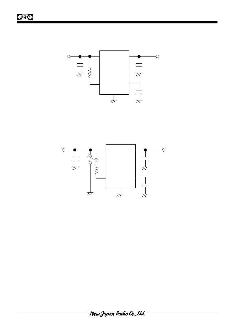
I TYPICAL APPLICATION
x
In the case where ON/OFF Control is not required:
Connect control terminal to V
IN
terminal
The quiescent current can be reduced by using a resistance "R". Instead, it increases the minimum
operating voltage. For further information, please refer to Figure "Output Voltage vs. Control Voltage".
y
In use of ON/OFF CONTROL:
State of control terminal:
∑"H" output is enabled.
∑ "L" or "open" output is disabled.
Noise bypass Capacitance Cp
Noise bypass capacitance Cp reduces noise generated by band-gap reference circuit.
Noise level and ripple rejection will be improved when larger Cp is used.
Use of smaller Cp value may cause oscillation.
Use the Cp value of 0.01uF greater to avoid the problem.
V
IN
V
OUT
CONTROL
NOISE
BYPASS
GND
Cp=0.01uF
1.0uF
OR
2.2uF(Vo<2.6V)
(Ceramic
Capacitor)
V
OUT
0.1uF
V
IN
R
(0~300k
)
V
IN
V
OUT
CONTROL
NOISE
BYPASS
GND
Cp=0.01uF
1.0uF
OR
2.2uF(Vo<2.6V)
(Ceramic
Capacitor)
V
OUT
0.1uF
V
IN
R
(0~300k
)
V
IN
V
OUT
CONTROL
NOISE
BYPASS
GND
Cp=0.01uF
1.0uF
OR
2.2uF(Vo<2.6V)
(Ceramic
Capacitor)
V
OUT
0.1uF
V
IN
R
V
IN
V
OUT
CONTROL
NOISE
BYPASS
GND
Cp=0.01uF
1.0uF
OR
2.2uF(Vo<2.6V)
(Ceramic
Capacitor)
V
OUT
0.1uF
V
IN
R


NJM2880
[CAUTION]
The specifications on this databook are only
given for information , without any guarantee
as regards either mistakes or omissions. The
application circuits in this databook are
described only to show representative usages
of the product and not intended for the
guarantee or permission of any right including
the industrial rights.