 | –≠–ª–µ–∫—Ç—Ä–æ–Ω–Ω—ã–π –∫–æ–º–ø–æ–Ω–µ–Ω—Ç: NJM3517 | –°–∫–∞—á–∞—Ç—å:  PDF PDF  ZIP ZIP |
NJM3517
STEPPER MOTOR CONTROLLER / DRIVER
s
GENERAL DESCRIPTION
s
PACKAGE OUTLINE
NJM3517 is a stepper motor controller/driver, which requires
minimum of external components and drive currents up to 500mA.
The NJM3517 is suited for applications requiring least-possible RFI.
Operating in a bi-level drive mode can increase motor performance;
high voltage pulse is applied to the motor winding at the beginning
of a step, in order to give a rapid rise of current.
s
FEATURES
∑ Internal complete driver and phase logic
∑ Continuous-output current 2 x 350mA
∑ Half- and full-step mode generation
∑ LS-TTL-compatible inputs
∑ Bi-level drive mode for high step rates
∑ Voltage-doubling drive possibilities
∑ Half-step position-indication output
∑ Minimal RFI
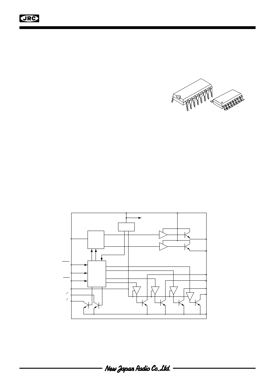
∑ Packages DIP16 / EMP16
s
BLOCK DIAGRAM
Figure 1. Block diagram
RC
STEP
DIR
HSM
INH
O
A
O
B
L
A
L
B
P
B2
P
B1
P
A2
P
A1
GND
V
CC
V
SS
NJM3517
POR
Mono
F - F
Phase
Logic
P
A
P
B
NJM3517E2
NJM3517D2
NJM3517
B2
B1
GND
A1
A2
DIR
STEP
B
V
V
L
L
R
INH
HSM
ÿ
1
2
3
4
5
6
7
8
16
15
14
13
12
11
10
9
P
P
P
P
A
C
A
B
SS
CC
ÿ
B2
B1
GND
A1
A2
DIR
STEP
B
V
V
L
L
R
INH
HSM
ÿ
1
2
3
4
5
6
7
8
16
15
14
13
12
11
10
9
P
P
P
P
A
C
A
B
SS
CC
ÿ
NJM
3517D2
NJM
3517E2
s
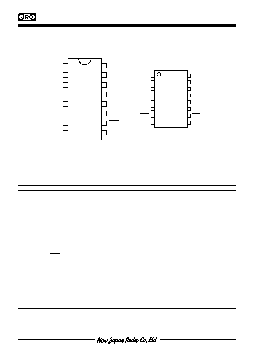
PIN CONFIGURATIONS
s
PIN DESCRIPTION
DIP
EMP-pack.
Symbol
Description
1
1
P
B2
Phase output 2, phase B. Open collector output capable of sinking max 500 mA.
2
2
P
B1
Phase output 1, phase B. Open collector output capable of sinking max 500 mA.
3
3
GND
Ground and negative supply for both V
CC
and V
SS
.
4
4
P
A1
Phase output 1, phase A.
5
5
P
A2
Phase output 2, phase A.
6
6
DIR
Direction input. Determines in which rotational direction steps will be taken.
7
7
STEP
Stepping pulse. One step is generated for each negative edge of the step signal.
8
8
ÿB
Zero current half step position indication output for phase B.
9
9
ÿA
Zero current half step position indication output for phase A.
10
10
HSM
Half-step mode. Determines whether the motor will be operated in half or full-step
mot. When pulled low, one step pulse will correspond to a half step of the motor.
11
11
INH
A high level on the inhibit input turns all phase output off.
12
12
RC
Bi-level pulse timing pin. Pulse time is approximately t
on
= 0.55 ∑ R
T
∑ C
T
13
13
LA
Second level (bi-level) output, phase A.
14
14
LB
Second level (bi-level) output, Phase B.
15
15
V
SS
Second level supply voltage, +10 to +40 V.
16
16
V
CC
Logic supply voltage, nominally +5 V.
Fugure 2.Pin configurations
NJM3517
s
FUNCTIONAL DESCRIPTION
The circuit, NJM3517, is a high performance motor driver, intended to drive a stepper motor in a unipolar, bi-level
way. Bi-level means that during the first time after a phase shift, the voltage across the motor is increased to a
second voltage supply, V
SS
, in order to obtain a more-rapid rise of current, see figure 25.
The current starts to rise toward a value which is many times greater than the rated winding current. This com-
pensates for the loss in drive current and loss of torque due to the back emf of the motor.
After a short time, t
On
, set by the monostable, the bi-level output is switched off and the winding current flows from
the V
MM
supply, which is chosen for rated winding current. How long this time must be to give any increase in
performance is determined by V
SS
voltage and motor data, the L/R time-constant.
In a low-voltage system, where high motor performance is needed, it is also possible to double the motor voltage
by adding a few external components, see figure 4.
The time the circuit applies the higher voltage to the motor is controlled by a monostable flip-flop and determined
by the timing components R
T
and C
T
.
The circuit can also drive a motor in traditional unipolar way.
An inhibit input (INH) is used to switch off the current completely.
s
LOGIC INPUTS
All inputs are LS-TTL compatible. If any of the logic inputs are left open, the circuit will accept it as a HIGH level.
NJM3517 contains all phase logic necessary to control the motor in a proper way.
STEP -- Stepping pulse
One step is generated for each negative edge of the STEP signal. In half-step mode, two pulses will be required to
move one full step. Notice the set up time, t
s
, of DIR and HSM signals. These signals must be latched during the
negative edge of STEP, see timing diagram, figure 6.
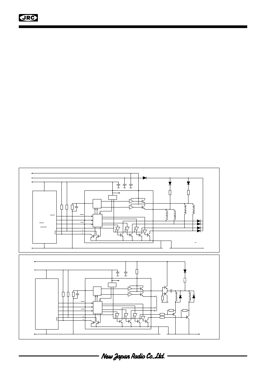
Figure 4.
Voltage
doubling with
external
transistors
Figure 3.
Typical
application
RC 12
STEP 7
DIR 6
HSM 10
INH 11
O
A
9
O
B
8
13 L
A
14 L
B
1 P
B2
2 P
B1
5 P
A2
4 P
A1
3 GND
V
CC
16
V
SS
15
NJM3517
PQR
Mono
F - F
Phase
Logic
P
A
P
B
STEP
CW / CCW
HALF / FULL STEP
NORMAL /INHIBIT
(Optional Sensor)
GND
V
CC
CMOS, TTL-LS
Input / Output-Device
V
SS
+ 5V
GND (V
CC
)
V
MM
R9
R8
R
T
C
T
C
3
C
4
C
5
+
+
+
R11
R10
D2
D1
MOTOR
D3-D6
D3-D6 are
UF 4001 or
BYV 27
trr < 100 ns
GND (V
MM
,V
SS
)
D3
+
RC 12
STEP 7
DIR 6
HSM 10
INH 11
O
A
9
O
B
8
13 L
A
14 L
B
1 P
B2
2 P
B1
5 P
A2
4 P
A1
3 GND
V
CC
16
V
SS
15
NJM3517
PQR
Mono
F - F
Phase
Logic
P
A
P
B
STEP
CW / CCW
HALF / FULL STEP
NORMAL /INHIBIT
(Optional Sensor)
GND
V
CC
CMOS, TTL-LS
Input / Output-Device
V
MM
+ 5V
GND (V
CC
)
R9
R8
R
T
C
T
C
3
C
4
+
+
R10
D1
1/2 MOTOR
GND (V
MM
,V
SS
)
R1
R2
Q1
Q3
C1
R12
R13
R4
R5
Q5
Q6
Equal to
Phase A
NJM3517
DIR -- Direction
DIR determines in which direction steps will be taken. Actual direction depends on motor and motor connections.
DIR can be changed at any time, but not simultaneously with STEP, see timing diagram, figure 6.
HSM determines whether the motor will be controlled in full-step or half-step mode. When pulled low, a step-
pulse will correspond to a half step of the motor. HSM can be changed at any time, but not simultaneously with
STEP, see timing diagram, figure 6.
INH -- Inhibit
A HIGH level on the INH input,turns off all phase outputs to reduce current consumption.
s
RESET
An internal Power-On Reset circuit connected to V
cc
resets the phase logic and inhibits the outputs during power
up, to prevent false stepping.
s
OUTPUT STAGES
The output stage consists of four open-collector transistors. The second high-voltage supply contains Darlington
transistors.
s
PHASE OUTPUT
The phase outputs are connected directly to the motor as shown in figure 3.
s
BI-LEVEL TECHNIQUE
The bi-level pulse generator consists of two monostables with a common RC network.
The internal phase logic generates a trigger pulse every time the phase changes state. The pulse triggers its own
monostable which turns on the output transistors for a precise period of time:
t
On
= 0.55 ∑ C
T
∑ R
T
.
See pulse diagrams, figures 7 through 11.
s
BIPOLAR PHASE LOGIC OUTPUT
The ÿ
A
and ÿ
B
outputs are generated from the phase logic and inform an external device if the A phase or the B
phase current is internally inhibited. These outputs are intended to support if it is legal to correctly go from a half-
step mode to a full-step mode without loosing positional information.
The NJM3517 can act as a controller IC for 2 driver ICs, the NJM3770A. Use P
A1
and P
B1
for phase control, and
ÿ
A
and ÿ
B
for I
0
and I
1
control of current turnoff.
NJM3517
s
ABSOLUTE MAXIMUM RATINGS
Parameter
Pin No.
Symbol
Min
Max
Unit
Voltage
Logic supply
16
V
CC
0
7
V
Second suppl
15
V
SS
0
45
V
Logic input
6, 7, 10, 11
V
I
-0.3
6
V
Current
Phase output
1, 2, 4, 5
I
P
0
500
mA
Second-level output
13, 14
I
L
-500
0
mA
Logic input
6, 7, 10, 11
I
I
-10
mA
The zero output
8, 9
I
-
6
mA
Temperature
Operating junction temperature
T
j
-40
+150
∞
C
Storage temperature
T
Stg
-55
+150
∞
C
Power Dissipation (Package Data)
Power dissipation at T
a
= 25
∞
C, DIP package. Note 2.
P
D
-
1.6
W
Power dissipation, EMP package. Note 3.
P
D
-
1.3
W
s
RECOMMENDED OPERATING CONDITIONS
Parameter
Symbol
Min
Typ
Max
Unit
Logic supply voltage
V
CC
4.75
5
5.25
V
Second-level supply voltage
V
SS
10
-
40
V
Phase output current
I
P
0
-
350
mA
Second-level output current
I
L
-350
-
0
mA
Operating junction temperature
T
J
-20
-
+125
∞
C
Set up time
t
s
400
-
-
ns
Step pulse duration
t
p
800
-
-
ns
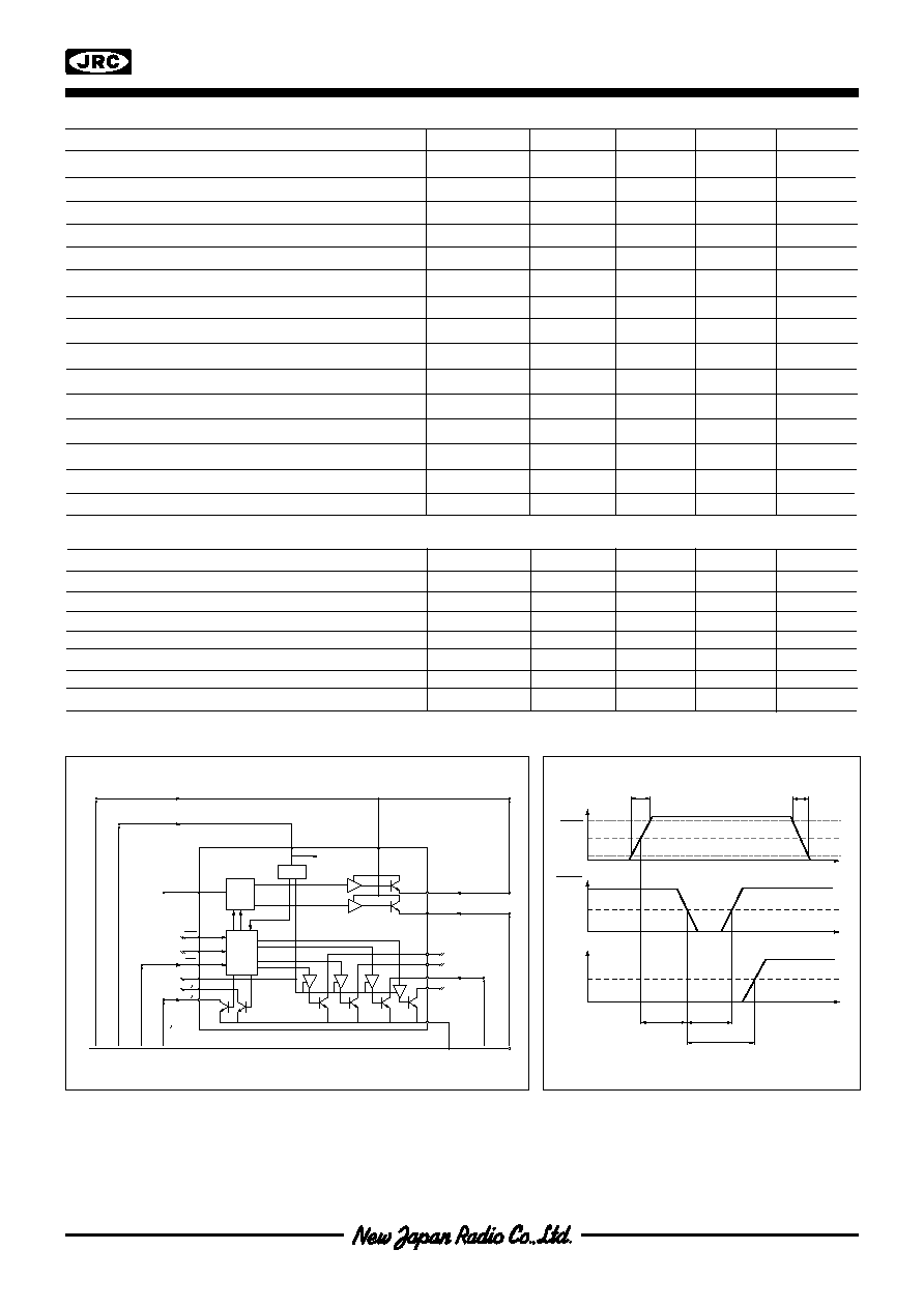
Figure 5. Definition of symbols
HSM
or
DIR
V
I
STEP
I
P
t
t
t
t
r
t
f
t
s
t
p
t
d
Figure 6. Timing diagram
RC 12
STEP 7
DIR 6
HSM 10
INH 11
O
A
9
O
B
8
13 L
A
14 L
B
1 P
B2
2 P
B1
5 P
A2
4 P
A1
3 GND
V
CC
16
V
SS
15
NJM3517
POR
Mono
F - F
Phase
Logic
P
A
P
B
V
CC
V
SS
V
I
V
IH
V
IL
V
OCE Sat
V
LCE Sat
V
L
V
PCE Sat
V
P
I
P
I
PL
I
LL
I
L
I
I
I
IL
I
IH
I
SS
I
CC