 | –≠–ª–µ–∫—Ç—Ä–æ–Ω–Ω—ã–π –∫–æ–º–ø–æ–Ω–µ–Ω—Ç: NJU26188 | –°–∫–∞—á–∞—Ç—å:  PDF PDF  ZIP ZIP |

NJU26100 Series
- 1 -
Ver.2005-02-24
NJU26100 Series Hardware Specification
General Description
This document describes the NJU26100 Series common hardware specifications.
This document is applied to the NJU26101 up to the NJU26199.
The individual function is described in the each data sheet. Please refer to the
each data sheet to find the detail functions. The firmware commands are
described in the each firmware document.
Hardware Specification
∑ 24bit Fixed-point Digital Signal Processing
∑ Maximum System Clock Frequency
: 38MHz
∑ Digital Audio Interface
: 3 Input ports / 3 Output ports
∑ Master / Slave Mode
∑ Master Mode MCK
:1/2 fclk, 1/3 fclk
ex. MCK = 384Fs(1/2) or MCK = 256Fs(1/3) at fclk=768Fs
∑ Two kinds of micro computer interface
I
2
C bus (standard-mode/100kbps)
Serial interface (4 lines: clock, enable, input data, output data)
∑ Power Supply
: 2.5V ( 3.3V Input tolerant )
∑
Package
:
QFP32-R1
Package
NJU26100 Series
TIMING
GENERATOR
PROGRAM
CONTROL
ALU
24-BIT x 24-BIT
MULTIPLIER
ADDRESS GENERATION UNIT
FIRMWARE
ROM
DELAY
RAM
DATA
RAM
SERIAL
HOST
INTERFACE
GPIO AND
CONFIGURATION
INTERFACE
SDO0
SDI0
SDI2
GPIO0
SCL/SCK
SDA/SDOUT
AD1/SDIN
AD2/SSb
XI
XO
RESETb
DSP ARITHMETIC UNIT
SDO1
BCKI
SDI1
MCK
BCKO
LRO
SERIAL AUDIO
INTERFACE
NJU26100 Series
SDO2
LRI
GPIO1
SERIAL OUT
SERIAL OUT
SERIAL OUT
SERIAL IN
SERIAL IN
SERIAL IN
NJU26100 Series
- 2 -
Ver.2005-02-24
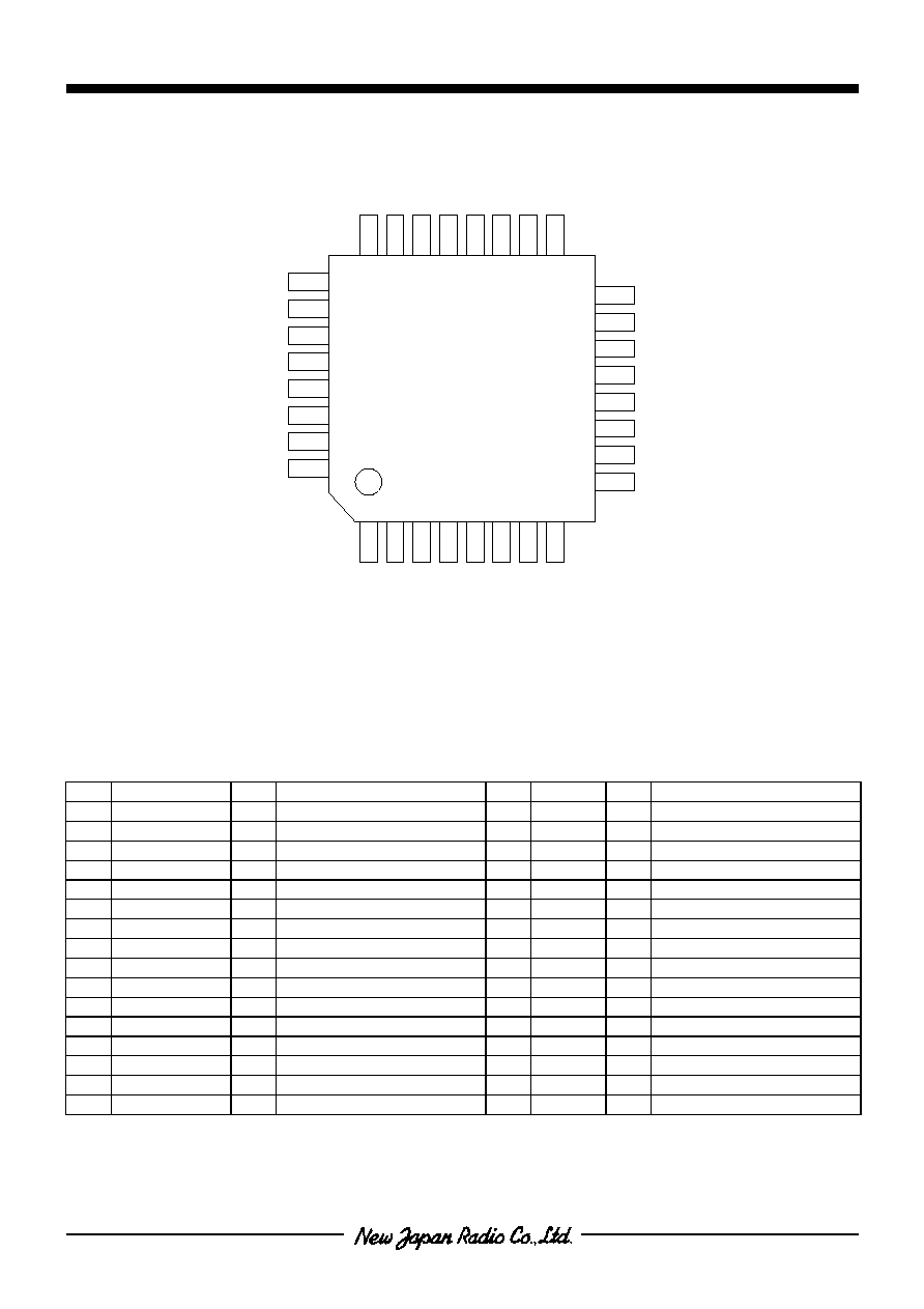
Pin Configuration
Pin Description
Pin Description
No. Symbol
I/O Description
No. Symbol I/O Description
1
SDO2
O
Audio Data Output CH2
17
VDDC
--
Core Power Supply +2.5V
2
SDO1
O
Audio Data Output CH1
18
VDDC
--
Core Power Supply +2.5V
3
SDO0
O
Audio Data Output CH0
19
VSSC
--
Core GND
4
GPIO0
I/O
General Purpose IO
20
VSSC
--
Core GND
5 SCL/SCK I I
2
C Clock / Serial Clock
21
VDDR
--
I/O Power Supply +2.5V
6 SDA/SDOUT I/O
I
2
C I/O / Serial Output
22
VDDR
--
I/O Power Supply +2.5V
7 AD1/SDIN I I
2
C Address / Serial Input
23
VSSR
--
I/O GND
8 AD2/SSb
I I
2
C Address / Serial Enable
24
VSSR
--
I/O GND
9
VDDO
--
OSC Power Supply +2.5V
25
SDI0
I
Audio Data Input CH0
10
XI
I
X'tal Clock Input
26
SDI1
I
Audio Data Input CH1
11
XO
O
OSC Output
27
SDI2
I
Audio Data Input CH2
12 VSSO
-- OSC
GND
28 LRI
I LR
Clock
Input
13
RESETb
I
RESET (active Low)
29
BCKI
I
Bit Clock Input
14
VDDC
--
Core Power Supply +2.5V
30
MCK
O
Master Clock Output
15
VSSC
--
Core GND
31
BCKO
O
Bit Clock Output
16
GPIO1
I/O
General Purpose IO
32
LRO
O
LR Clock Output
*1 I : Input, O : Output, I/O : Bi-directional
*2 SDI0, SDI1, SDI2, SDO0, SDO1, SDO2, GPIO0, GPIO1 are different by any function. Refer to each datasheet.
SD
O
2
SD
O
1
SD
O
0
GPIO0
SC
L
/
SC
K
S
DA/S
D
O
U
T
AD
1
/
S
D
I
N
AD
2
/
S
S
b
1
2
3
4
5
6
7
8
2
4
2
3
2
2
2
1
2
0
1
9
1
8
1
7
9
10
11
12
13
14
15
16
32
31
30
29
28
27
26
25
NJU26100
Series
V
DDC
V
DDC
VS
S
C
V
DDR
V
DDR
VS
S
R
VS
S
R
VDDO
XI
XO
VSSO
RESETb
VDDC
VSSC
GPIO1
SDI0
VS
S
C
SDI1
SDI2
LRI
BCKI
MCK
BCKO
LRO
NJU26100 Series
- 3 -
Ver.2005-02-24
1. Electric Characteristics
1.1 Absolute Maximum Ratings
Table1-1 Absolute Maximum Ratings
(V
SSO
=V
SSC
=V
SSR
=0V, Ta=25
∞C)
Parameter Symbol
Rating
Units
Supply Voltage
V
DD
0 to 3.05
V
XI Input Voltage
V
x(OSC)
-0.3 to V
DD
V
Input Pin Voltage
V
x(IN)
-0.3 to 3.6
V
Power Dissipation
P
D
0.3 W
Storage Temperature
T
stg
-40
to
+125
∞C
*
1
They apply SCL/SCK, AD1/SDIN, AD2/SSb, RESETb, SDI0, SDI1, SDI2, LRI, and BCKI pin. It applies to GPIO0
(SEL1) pin of NJU26100 series except NJU26150. However, it applies to SDA/SDOUT pin at the time of I
2
C
mode operation.
NJU26100 Series
- 4 -
Ver.2005-02-24
1.2 Electric Characteristics
Table1-2 Electric Characteristics
(V
DDO
=V
DDC
=V
DDR
=2.5V, V
SSO
=V
SSC
=V
SSR
=0V, Ta=25
∞C)
Parameter Symbol
Test
Condition
Min.
Typ.
Max.
Units
Operating V
DD
Voltage
V
DD
V
DDO
, V
DDC
, V
DDR
pin
2.25
2.5
2.75
V
Operating Current
I
DD
f
OSC
=36.864MHz -
40
-
mA
Operating Temperature
T
OPR
-40
25 85
∞C
Recommended Operating
Temperature
T
OPRR
V
DDO
=V
DDC
=V
DDR
=2.5V
-10
25
70
∞C
High Level Input
Voltage (XI)
V
IH(OSC)
XI
pin
2.0
-
V
DD
V
High Level Input Voltage
V
IH
2.0
-
3.3
V
Low Level Input Voltage
V
IL
V
SS
=V
SSO
=V
SSC
=V
SSR
V
SS
- 0.5
V
High Level Input Current
I
IH
V
IN
=3.3V
expect for GPIO pin
-10 -
+10
µA
High Level Input Current
I
IH(pd)
V
IN
=3.3V
GPIO pin Only
100 - 300
µA
Low Level Input Current
I
IL
V
IN
=V
SSO
=V
SSC
=V
SSR
-10 -
+10
µA
High Level Output Voltage
V
OH
I
OH
=-2mA
I
OH
=-100
µA
V
DD
-0.4
V
DD
-0.1
- - V
Low Level Output Voltage
V
OL
I
OL
=2mA -
-
0.4
V
Input Capacitance
C
IN
-
5
- pF
Input Rise/Fall transition Time
t
r
/ t
f
except for SCL/SCK,
SDA/SDOUT,
AD1/SDIN, AD2/SS
pin*
1
- -
100
ns
Clock Frequency
f
OSC
XI
pin
-
- 38.0 MHz
Ext.System Clock Duty Cycle
r
EC
XI
pin
47.5 50 52.5 %
*
1
The tr / tf of these pins are specified separately.
*
2
All input / input-and-output pins serve as the Schmidt trigger input except for XI pin.
Input
pin
Output
pin
XI
/
XO
pin
(GPIO0, SCL/SCK, SDA/SDOUT,
(SDO0, SDO1, SDO2, GPIO0,
(XI, XO)
AD1/SDIN, AD2/SSb, RESETb, GPIO1,
*
3
SDA/SDOUT, GPIO1, MCK,
SDI0, SDI1, SDI2, LRI, BCKI pin)
BCKO, LRO pin)
Fig.1- 1 I/O Equivalent Circuits
*
3
SDA becomes Open-Drain at the time of the output of I
2
C.
Input
pin
V
DDR
VDDC
V
SSC
V
DDR
V
SSR
Output
pin
V
DDC
V
DDO
XO
pin
V
SSO
V
SSC
XI
pin
NJU26100 Series
- 5 -
Ver.2005-02-24
2. Clock and Reset
The NJU26100 Series XI pin requires the system clock that should be related to the sample frequency Fs. The
XI/XO pins can generate the system clock by connecting the crystal oscillator or the ceramic resonator.
When the external oscillator is connected to XI/XO pins, check the voltage level of the pins. Because the
maximum input voltage level of XI pin is deferent from the other input or bi-directional pins. The maximum
voltage-level of XI pin equals to V
DD
.
To initialize the NJU26100 Series, RESETb pin should be set Low level during some period. After some period of
Low level, RESETb pin should be High level. This procedure starts the initialization of the NJU26100 Series.
To select I
2
C bus or 4-Wire serial bus, some level should be supplied to GPIO0 pin (SEL1 pin). When GPIO0 pin
(SEL1 pin)="Low", I
2
C bus is selected. When GPIO0 pin (SEL1 pin)="High", 4-Wire serial bus is selected. The level
of GPIO0 pin (SEL1 pin) is checked by the NJU26100 Series in 1 m sec after RESETb pin level goes to "High".
After the power supply and the oscillation of the NJU26100 Series becomes stable, RESETb pin should be kept
Low-level more than t
RESETb
period.
Fig. 2- 1 Reset Timing
Table 2- 1 Reset Time
Notice :
Please consult with manufacture of crystal oscillator / ceramic resonator enough in use of these parts.
NJRC would not take the responsibility on the external parts of clock generating.
Symbol Time
t
RESETb
1µs
OSC unstable
OSC stable
XI
V
DD
RESETb
t
RESETb