 | ÐлекÑÑоннÑй компоненÑ: NJU26901 | СкаÑаÑÑ:  PDF PDF  ZIP ZIP |
Äîêóìåíòàöèÿ è îïèñàíèÿ www.docs.chipfind.ru
NJU26901
- 1 -
Ver.2004-06-24
Digital Audio Delay
!
General Description
The NJU26901 is a digital audio delay. The NJU26901 provides delay-time
adjustment function and digital audio interface.
!
FEATURES
·
2-Channel Audio Delay (24 bits data width).
Delay Time 85msec at fs = 48kHz ( 128msec at fs = 32kHz , 43msec at fs = 96kHz)
·
4 delay time modes( ¼, ½, ¾, 1 max. delay ) are selectable without a micro-computer.
·
To make long delay time, the NJU26901 can be connected serially.
·
Non-audio-signal data can be delayed by the NJU26901.
!
Hardware Specification
·
Digital Audio Interface
:
1 Input port / 1 Output port
·
Digital Audio Format
:
I
2
S 24bit BCK : 64fs, Slave Mode
·
Audio Bit Clock (BCK) Frequency :
13MHz Max ( approximate fs=200KHz)
·
Package
:
EMP8 Pb-Free
·
Power Supply
:
2.5V ( +3.3V input tolerant )
!
Package
NJU26901E2
NJU26901
- 2 -
Ver.2004-06-24
!
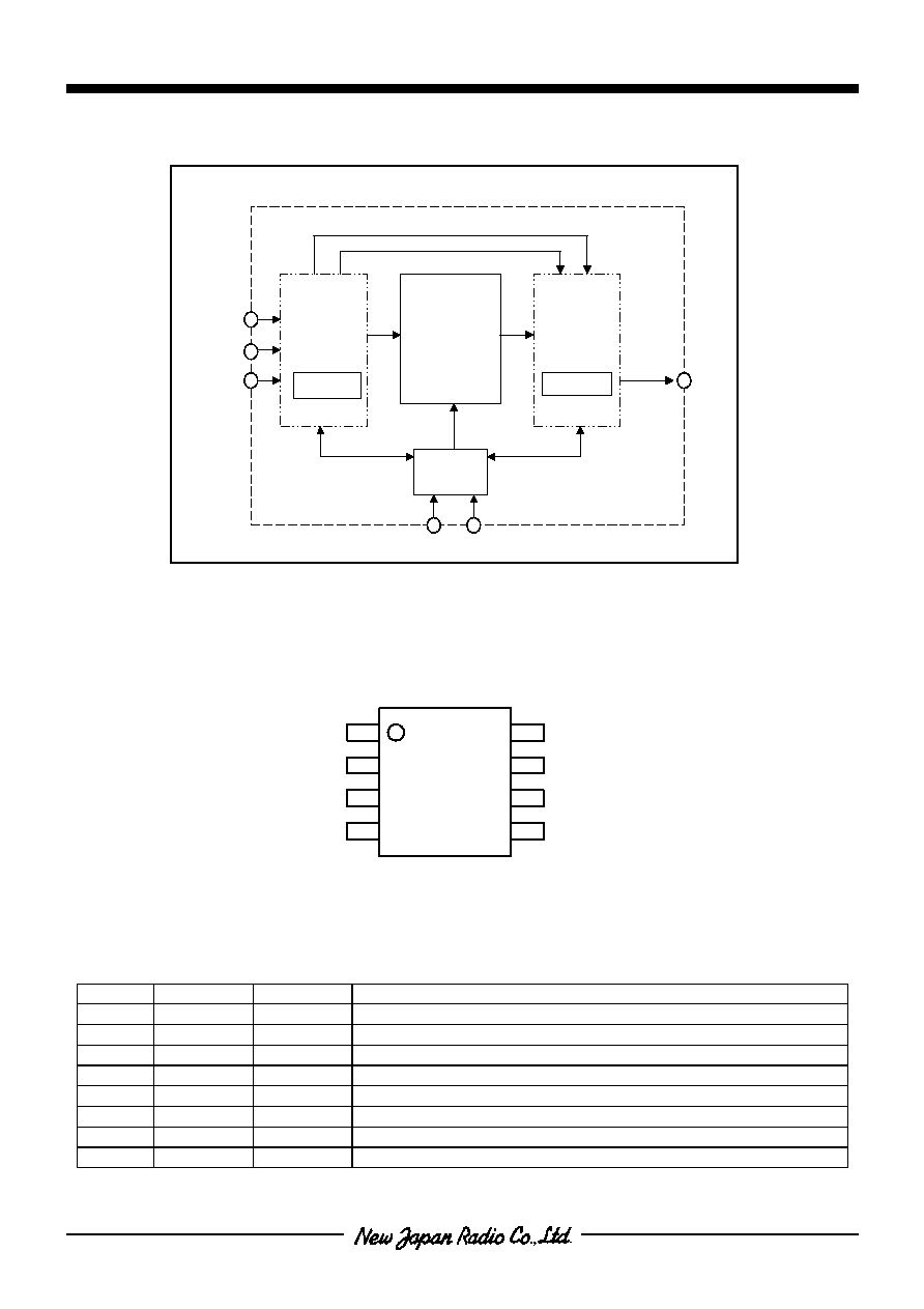
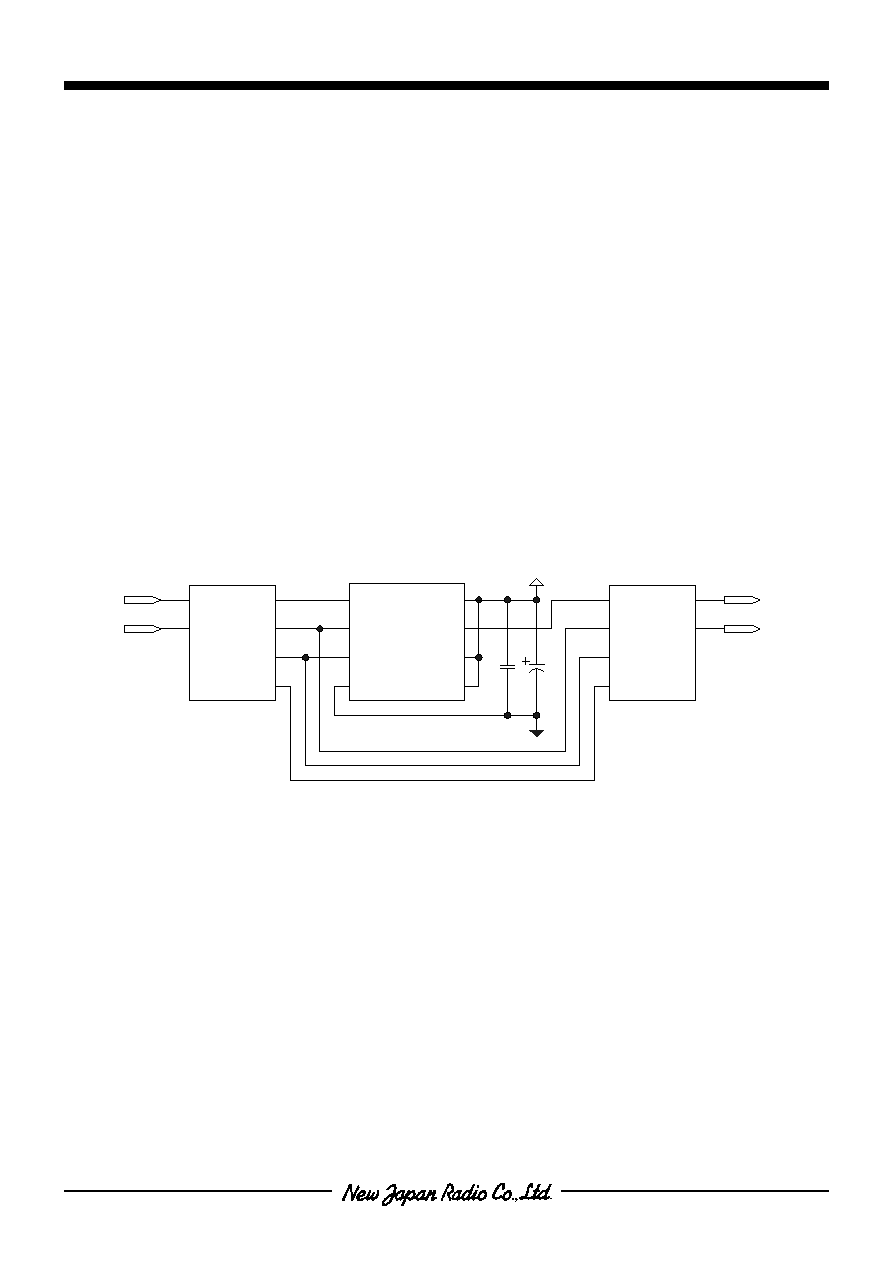
Function Block Diagram
Fig. 1 Function Block Diagram
!
Pin Assignment
NJU26901
1
5
6
7
8
4
3
2
SDI
VDD
SDO
COUNT[1]
COUNT[0]
VSS
BCKI
LRI
Fig. 2 Pin Assignment
!
Pin Description
Table 1 Pin Description
No. Symbol I/O
Description
1
SDI
I
Audio Data Input
2
LRI
I
LR Clock Input
3
BCKI
I
Bit Clock Input
4 VSS G
GND
5
COUNT[0]
I*
Delay Time Control 0
6
COUNT[1]
I*
Delay Time Control 1
7
SDO
O
Audio Data Output
8
VDD
P
Power Supply +2.5V
I : Input, I* : Input(internal pull-up), O : Output, P: +Power, G : GND
SDO
SDI
Control
Logic
Delay RAM
BCKI
SERIAL AUDIO
INTERFACE
LRI
BCKI
LRI
COUNT[1:0]
L/R
L/R in
NJU26901
SERIAL AUDIO
INTERFACE
NJU26901
- 3 -
Ver.2004-06-24
!
Absolute Maximum Ratings
Table 2 Absolute Maximum Ratings
Parameter Symbol
Rating
Units
Power Supply Voltage
V
DD
-0.3 to +3.0
V
Input Pin Voltage
V
TM
-0.3 to +3.6
V
Power Dissipation
P
D
100
mW
Storage Temperature
T
STR
-40
to
+125
°
C
!
Electric Characteristics
Table 3 Electric Characteristics (V
DD
=2.5V,Ta=25
)
Parameter Symbol
Test
Condition
Min.
Typ.
Max.
Units
Operating V
DD
Voltage
V
DD
2.25 2.5 2.75 V
Operating Current
I
DD
BCKI:13MHz
SDO:C
L
=25pF
- 1.0 - mA
Operating Temperature
T
OPR
-40 25 85
High Level Input Voltage
V
IH
2.0 - 3.3 V
Low Level Input Voltage
V
IL
-
- 0.5 V
High Level Output Voltage
V
OH
I
OH
= -2mA
I
OH
= -100uA
V
DD
-0.4
V
DD
-0.1
-
-
-
-
V
Low Level Output Voltage
V
OL
I
OL
= 2mA
I
OL
= 100uA
-
-
-
-
0.4
0.1
V
Input Current
I
IN
V
IN
= V
SS
3.6V
-15 - +15
uA
Input Current
I
IN(PU)
V
IN
= V
SS
3.6V
-100 - +15 uA
Input Capacitance
C
IN
- 10 - pF
Input Rise/Fall transition Time
t
r
/ t
f
-
- 100 ns
!
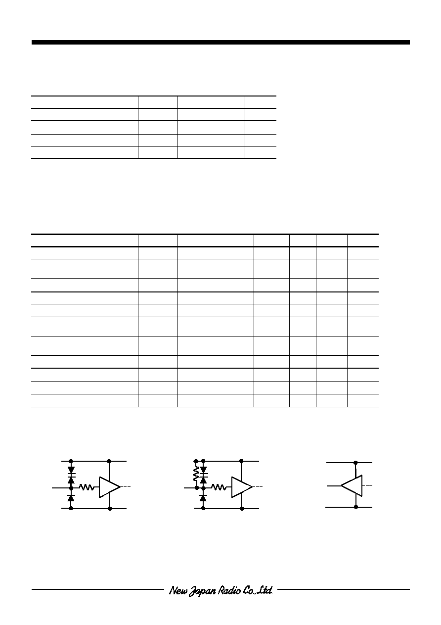
Equivalent Circuit
Input Pin #1,2,3
Input Pin #5,6
Output Pin #7
Fig. 3 Input Terminal Equivalent Circuit
Output
terminal
VDD
VSS
Input
terminal
VDD
VSS
Input
terminal
VDD
VSS
NJU26901
- 4 -
Ver.2004-06-24
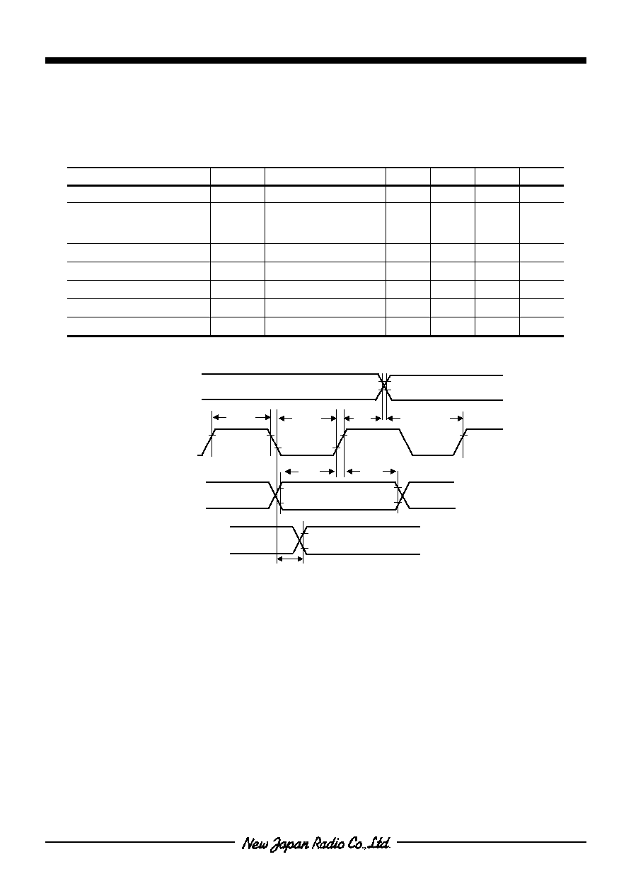
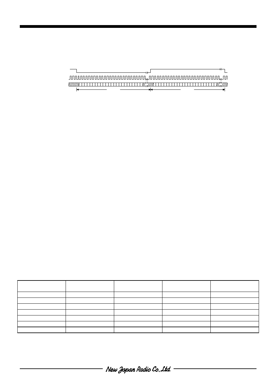
LRI
BCKI
t
DS
t
DH
t
SIH
t
LSI
t
SIL
t
SLI
SDI
SDO
t
DOD
!
Serial Audio Timing
Table 4 Serial Audio Input Timing Parameters
Parameter Symbol
Test
Condition
Min
Typ.
Max
Units
BCKI Frequency
f
BCK
-
-
13
MHz
BCKI Period
L Pulse Width
H Pulse Width
t
SIL
t
SIH
35
35
- - ns
BCKI to LRI Time
T
SLI
15
-
-
ns
LRI to BCKI Time
t
LSI
15
-
-
ns
Data Setup Time
t
DS
15
-
-
ns
Data Hold Time
t
DH
15
-
-
ns
Data Output Delay
t
DOD
SDO:C
L
=25pF -
15
ns
Fig. 4 Serial Audio Input / Output Timing
NJU26901
- 5 -
Ver.2004-06-24
!
Serial Audio Interface
Digital Audio format is I
2
S 24bit 64fs in fig. 5. The input and output format are the same I
2
S 24bit 64fs.
Fig 5 Digital Audio Format (I
2
S 24bits 64fs)
!
Function Description
·
SDI(#1) is serial audio input pin. The input audio data should be connected to this pin. The NJU26901 fetches
in the input audio data every LRI edge.
·
LRI(#2) is LR clock input pin. This LR clock frequency is the same frequency of the input audio signal.
LRI="Low" shows SDI and SDO data are left channel data. LRI="High" shows SDI and SDO data are right
channel data.
·
BCKI(#3) is bit clock input pin. This BCKI clock frequency is 64 times as large as the input audio signal.
·
SDO(#7) is serial audio output pin. The delayed audio data come out through this pin.
·
VDD(#8) is 2.5V power supply pin. VSS(#4) is GND pin. The decoupling capacitor is necessary between VDD
and VSS.
·
The input pins can interface to 3.3V ICs. The output pins can interface to 2.5V ICs. Refer to table3 "Electric
Characteristics".
·
After Power-on RESET, there is possibility the NJU26901 generates random data for the delay time period set
by COUNT[0],[1] pins. If necessary, the mute circuit should be added.
!
Delay Time
·
The NJU26901 provides maximum 4097 samples delay and slave-mode audio interface. The delay time
depends on sampling frequency.
·
Delay time is controlled by COUNT[0], COUNT[1]. Table 5 shows Delay Time vs Sampling Frequency.
·
Detail delay time is evaluated by the following formula.
Delay time = {1/(fs)}
×
(sampling number + 1) [sec]
·
The sampling number is incremented every LRI clock.
Table 5 Delay Time vs Sampling Frequency
Sampling Frequency
(fs)
4/4
(COUNT[1:0]=11)
3/4
(COUNT[1:0]=01)
1/2
(COUNT[1:0]= 10)
1/4
(COUNT[1:0]= 00)
192KHz 21ms 16ms 11ms 5ms
96KHz 43ms 32ms 21ms 11ms
88.
2
KHz
47ms 35ms 23ms 12ms
48KHz 85ms 64ms 43ms 21ms
44.1KHz
93ms 69ms 46ms 23ms
32KHz 128ms 96ms 64ms 32ms
Sampling
number
(4097) (3073) (2049) (1025)
23
22
21
20
19
18
17
16
15
14
13
12
11
10
9
8
7
6
5
4
3
2
1
0
23
22
21
20
19
18
17
16
15
14
13
12
11
10
9
8
7
6
5
4
3
2
1
0
Left Channel
Right Channel
MSB
MSB
LSB
LSB
32 Clocks
32 Clocks
LRI
BCKI
SDI, SDO
NJU26901
- 6 -
Ver.2004-06-24
!
Change Delay Time Setting
The delay-time is set by COUNT[0],[1]. The delay-time can be changed during the NJU26901 operation.
In case the delay-time setting is changed, the NJU26901 sets up the new delay-time and initializes itself again
within 2 BCKI rising edge.
After setting the new delay-time, the NJU26901 holds SDO low-level, mute, during the new delay-time period.
After mute, the audio data come out through SDO.
The NJU26901 discards the input data which come during new delay-time setting period.
!
Application block diagram
NJU26901
1
SDI
LRI
BCKI
COUNT[0]
COUNT[1]
Delay Time = 85msec @ fs=48KHz
(COUNT[0:1]=11)
VSS
3
2
4
SDO
VDD
ADC
DATA OUT
BIT CLK OUT
LR CLK OUT
MASTER CLK OUT
ANALOG LIN
ANALOG RIN
MASTER CLK IN
LR CLK IN
BIT CLK IN
DATA IN
DAC
5
6
7
8
ANALOG ROUT
ANALOG LOUT
2.5V
10uF
0.1uF
Fig. 6 Application Block Diagram
NJU26901
- 7 -
Ver.2004-06-24
!
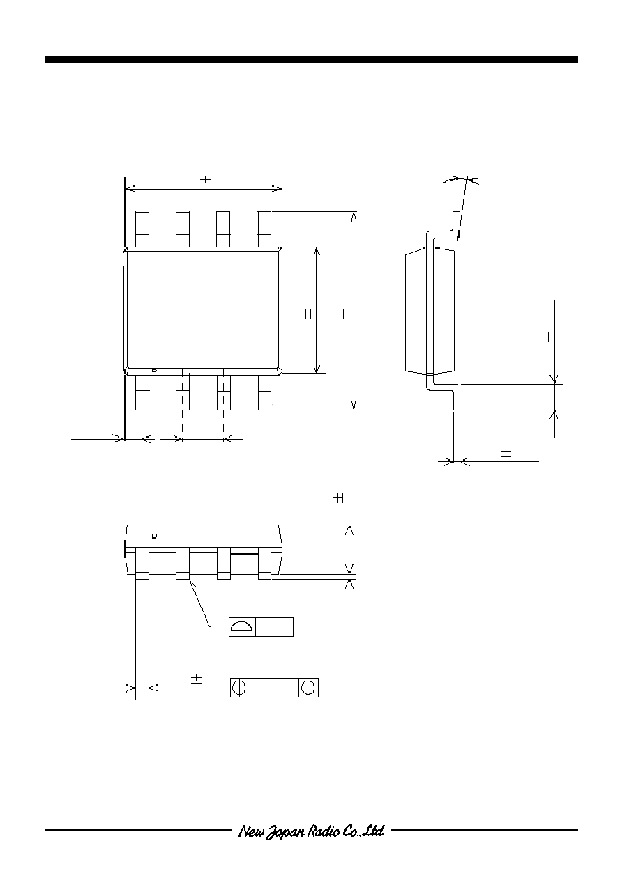
Package Dimensions
EMP8
3.9
0.1
6.0
0.2
0.65
0.
25
0.20 0.05
1.5
0.1
0.15
+0
.
1
-0.
0
5
0.10
4.9
0.1
0.15
M
0.40
0.1
0 - 10
o
1.27
0.6MAX
1
4
5
8
Unit
Fig. 7 Package Dimensions
NJU26901
- 8 -
Ver.2004-06-24
Version V1.11
[CAUTION]
The specifications on this databook are only
given for information , without any guarantee
as regards either mistakes or omissions. The
application circuits in this databook are
described only to show representative usages
of the product and not intended for the
guarantee or permission of any right including
the industrial rights.