- 1 -
NJU6052
Ver.2004-02-26
White LED Driver with Automatic Dimming Control
!
GENERAL DESCRIPTION
The NJU6052 is a white LED driver with an automatic
dimming control. It contains an output driver, a PWM
controller, a luminance sensor control (power supply for
sensor & A/D converter), a step-up DC/DC converter, a serial
interface, etc.
The output driver ensures a 60mA maximum capability
which allows the connection of 12 white LEDs (4 series x 3
parallels). Depending on the ambient light sensed with an
external luminance sensor, the PWM controller controls
PWM duty in 8 steps preselected out of 64 steps. In addition,
the frequency of the DC/DC converter is high so that it
permits the use of small, low-profile inductors and capacitors
to minimize the footprint in space-conscious applications.
All of these benefits make the NJU6052 suitable for the
battery-powered portable applications such as a cellular
phone, a camcorder, PDA, etc.
!
FEATURES
#
Drives up to 12 white LEDs (4 series x 3 parallels)
V
SW
= 18.0V(Max.), I
OUT
= 60mA
#
Built-in PWM Dimming Control
(Selectable 8 out of 64 steps)
#
Built-in Luminance Sensor Control (Power Supply for Sensor & A/D converter)
(No MPU-access required after initial setting)
#
Built-in Temperature Compensation Circuit to Suppress the Characteristic Degradation of LEDs
#
Uses Small Inductor and Capacitors
#
1.8V to 3.6V Operating Voltage for Logic Circuits (V
DDL
)
#
3.0V to 5.5V Operating Voltage for Step-up Circuits (V
DD
)
#
CMOS Technology
#
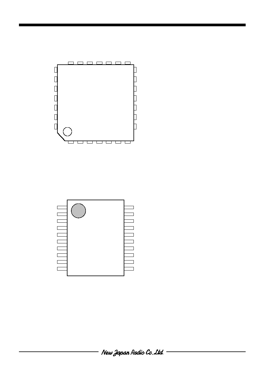
Package
: QFN28 / SSOP20
PRELIMINARY
!
PACKAGE OUTLINE
NJU6052KN1
NJU6052V
- 3 -
NJU6052
Ver.2004-02-26
!
PIN DESCRIPTION
No.
QFN
SSOP
SYMBOL
TYPE
DESCRIPTIONS
4 6
V
DD
Power
V
DD
Power Supply
- Power supply for step-up voltage
5 7
V
DDL
Power
V
DDL
Power Supply
- Power supply for logic voltage.
- Relation:1.8V
V
DDL
V
DD
should be maintained.
25
26
27
1
2
3
SW
Input
Switch
- All these terminals should be connected together.
10 10
SCK
Input
Shift Clock
- Serial data is latched on the rising edge of SCK.
9 9 DATA
Input / Output Serial Data
2 4 TEST
Output
Test
- This terminal must be open.
6 8
REQ
Input
Data Request
"L" : Writing command data
"H" : Reading sensor data
12 12
SENS
Input
Luminance Sensor Connection
11 11
RSTb
Input
Reset
- Active "L".
24 20
V
OUT
Input
Input
- This terminal is connected to LED anode.
23 19
FB
Input
Feedback
18
19
20
16
17
18
V
SS
Power
Ground
- All these terminals should be connected together.
16 14 CX/TCLK
Input
Oscillator Capacitor Connection / External Clock Input
13 13
V
SO
Output
V
SO
Power Supply
- Power supply for luminance sensor
- 2.4V typical
17 15
REF
Input
Reference Voltage
- This terminal must be open.
1
3
7
8
14
15
21
22
28
5
NC
-
Non Connection
- These terminals must be open.

- 5 -
NJU6052
Ver.2004-02-26
!
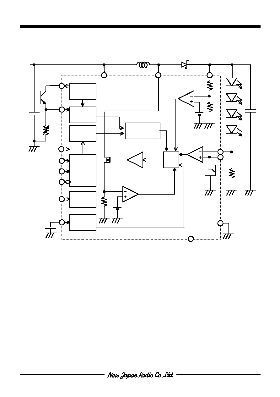
FUNCTIONAL DESCRIPTONS
(1) LED CURRENT CONTROL
The NJU6052 incorporates the LED current control circuit to regulate the LED current (I
LED
), which is
programmed by the feedback resistor (R
LED
) connected between the FB and V
SS
terminals. The reference voltage
V
REF
is internally regulated to 0.6V typical and connected to the positive input of the built-in comparator A1.
Formula (1) is used to choose the value of the R
LED
, as shown below.
V
REF
=0.6V (TYP.)
Referring to the block diagram is recommended for understanding the operation of the LED current control.
The I
LED
is the constant current programmed by the R
LED
. When the feedback voltage on the FB terminal reaches
above the reference voltage V
REF
on the REF terminal (i.e., I
LED
is above the level programmed by R
LED
), the
output capacitor C2 delivers the I
LED
. Once the feedback voltage drops below the reference voltage (i.e., I
LED
drops below the level programmed by R
LED
), the comparator A1 detects it and turns on the internal MOS switch,
then the current of the inductor L1 begins increasing. When this switch current reaches 720mA and the
comparator A2 detects it, or when the predetermined switch-on-period expires, the MOS switch is turned off.
The L1 then delivers current to the output through the diode D1 as the inductor current drops. After that, the MOS
switch is turned on again and the switch current increases up to 720mA. This switching cycle continues until the
I
LED
reaches the level programmed by the R
LED
, then the I
LED
is maintained constant.
When the feedback voltage is less than 1/2*V
REF
, the current limit of the MOS switch is reduced to 500mA
typical. This action reduces the average inductor-current, minimizes the power dissipation and protects the IC
against high current at start-up.
The total forward-voltage of the LEDs must be greater than the power supply voltage V
DD
, otherwise the
LEDs remain lighting up, being out of control.
(2) OSCILLATOR
The built-in oscillator incorporates a reference power supply, so its frequency is independent from the V
DD
.
The frequency is varied by the external capacitor CX, as shown in Figure 7.
(3) LUMINANCE SENSOR CONTROL
The luminance sensor control circuits consist of the power supply for sensor and the A/D converter. The A/D
converter senses the voltage on the SENS terminal and selects 1 out of 8 registers (PWM REGISTER 0≠7). And
the data in the selected register is reflected to the PWM duty (PWM dimming control). The contents of the
registers can be programmed through the serial interface, in other words, the dimming control is user-settable.
The voltage sense and the register selection are updated at regular intervals, and the interval period is set by
the "DIVIDE" bits. The selected register is held by setting "1" at the "HOLD" bit of the command data.
LED
REF
LED
I
V
R
=
--- Formula (1)