2002/03/11 ( 1 / 4 )
NJU6343
50MHz VCXO IC
s
GENERAL DESCRIPTION
The NJU6343 is a single chip C-MOS IC for VCXO that
consists of an oscillation amplifier and 3-state output buffer.
The NJU6343 integrates all components used in VCXO
module, and there is no need for completing VCXO module to
prepare any external components except a quartz crystal.
It can vary its output frequency by controlling voltage at V
C
terminal.
The oscillation amplifier is realized very low stand-by current
using NAND circuit.
The 3-state output buffer is C-MOS compatible.
s
FEATURES
q
Operating Voltage
2.7 to 3.6V
q
Maximum Oscillation Frequency
50MHz(T.B.D.)
q
Frequency Pulling Range
�
100ppm
q
Low Operating Current
q
High Fan-out
I
OH
/I
OL
= T.B.D @3.0V
q
Oscillation Stop and Output Stand-by Function
q
3-State Output Buffer
q
A Variable Capacitor on-chip
q
Package Outline
Chip
q
C-MOS Technology
s
COORDINATES
Starting Point:Chip Center Unit[um]
Chip Size:1.6x1.6mm
Thin-Chip Thickness:260
�
20um
Pad Size:90x90um
s
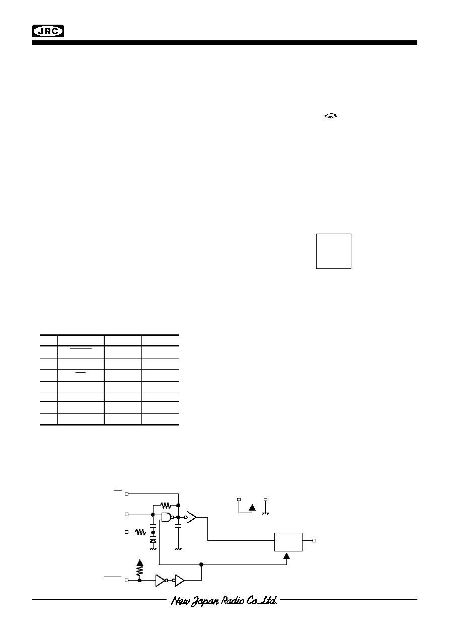
BLOCK DIAGRAM
No Pad
Name
X
Y
1
CONT
2 XT
3
XT
4 V
SS
F
OUT
V
C
V
DD
Product Specification
NJU6343C
s
PACKAGE OUTLINE
s
PAD LOCATION
CONT
XT
XT
Cg
Cd
Rf
BUFFER
STATE
3
-
OUT
F
DD
V
SS
V
VC
2002/03/11 ( 2 / 4 )
NJU6343
s
TREMINAL DESCRIPTION
SYMBOL
FUNCTION
CONT
Oscillation and 3-state Output Buffer Control
CONT
F
OUT
H or OPEN
Frequency Output corresponding to Control
Voltage.
L
Oscillation Stop and High impedance Output
XT
XT
Quartz Crystal Connecting Terminals
V
SS
V
SS
=0V
F
OUT
Frequency
Output
V
C
Frequency
Control
V
DD
V
DD
=3.0V
s
ABSOLUTE MAXIMUM RATINGS (Ta=25�C)
PARAMETER SYMBOL
RATING UNIT
Supply Voltage
V
DD
-0.5
to
+7.0 V
Control Voltage
V
C
V
SS
-0.5 to V
DD
+0.5 V
Input Voltage
V
IN
V
SS
-0.5 to V
DD
+0.5 V
Output Voltage
V
O
-0.5
to
V
DD
+0.5 V
Input Current
I
IN
�
10
mA
Output Current
I
O
�
25
mA
Operating Temperature Range
Topr
-40 to +85
�C
Storage Temperature Range
Tstg
-55 to +125
�C
Note1) If the supply voltage(V
DD
) is less than 7.0V, the input voltage must not over the V
DD
level though 7.0V is
limit specified.
Note2) Decupling capacitor should be connected between V
DD
and V
SS
due to the stabilized operation for the
circuit.
2002/03/11 ( 3 / 4 )
NJU6343
s
ELECTRICAL CHARACTERISTICS
(Ta=25�C)
PARAMETER SYMBOL
CONDITIONS
MIN TYP MAX
UNIT
Operating Voltage
V
DD
2.7
3.6 V
s
ELECTRICAL
CHARACTERISTICS
(V
DD
=3.0, V
C
=V
DD
/2, Ta=25�C)
PARAMETER SYMBOL
CONDITIONS
MIN TYP MAX
UNIT
Operating Current
I
DD
fosc=16MHz,
V
C
=V
DD
/2, C
L
=15pF T.B.D mA
Oscillation Stopping
Current
I
STB
CONT =V
SS
, V
C
=V
DD
/2, No load
2 5
uA
Stand-by Current
Ist
CONT XT=V
SS
, V
C
=V
DD
/2,
No load Note3)
1
uA
V
IH
2.4
3.0 V
Input Voltage
V
IL
0
0.6 V
I
OH
V
OH
=2.7V T.B.D
mA
Output Current
I
OL
V
OL
=0.3V T.B.D
mA
CONT =0.8V
DD
10 15
uA
Input Current
I
IN
CONT =0.2V
DD
1.8
3.0
uA
3-state Off Leakage
Current
I
OZ
CONT =V
SS
, V
C
=V
DD
/2,
F
OUT
= V
DD
or V
SS
�
0.1
uA
Feedback Resistance
Rf
Preliminary
T.B.D k
Internal Capacitor
Cg/Cd
fosc=16MHz
T.B.D
pF
Control Voltage
V
C
0
V
DD
V
Frequency Pulling
Range
f
C
V
C
=0 to V
DD
-100
+100
ppm
Maximum Oscillation
Frequency
F
MAX
50
MHz
C
L
=15pF, V
C
=V
DD
/2, @V
DD
/2
45 50 55
Output Signal
Symmetry
SYM
C
L
=30pF, V
C
=V
DD
/2, @V
DD
/2
45 50 55
%
C
L
=15pF, V
C
=V
DD
/2, 10% to 90%
3
6
Output Signal Rise
Time
tr
C
L
=30pF, V
C
=V
DD
/2, 10% to 90%
3
6
ns
C
L
=15pF, V
C
=V
DD
/2, 90% to 10%
3
6
Output Signal Fall
Time
tf
C
L
=30pF, V
C
=V
DD
/2, 90% to 10%
3
6
ns
Output Disable time
T
PLZ
C
L
=15pF, V
C
=V
DD
/2, R
UP
=10k
200
ns
Output Enable Time
T
PZL
C
L
=15pF, V
C
=V
DD
/2, R
UP
=10k
200
ns
Note3) Excluding input current on CONT Terminal.
2002/03/11 ( 4 / 4 )
NJU6343
s
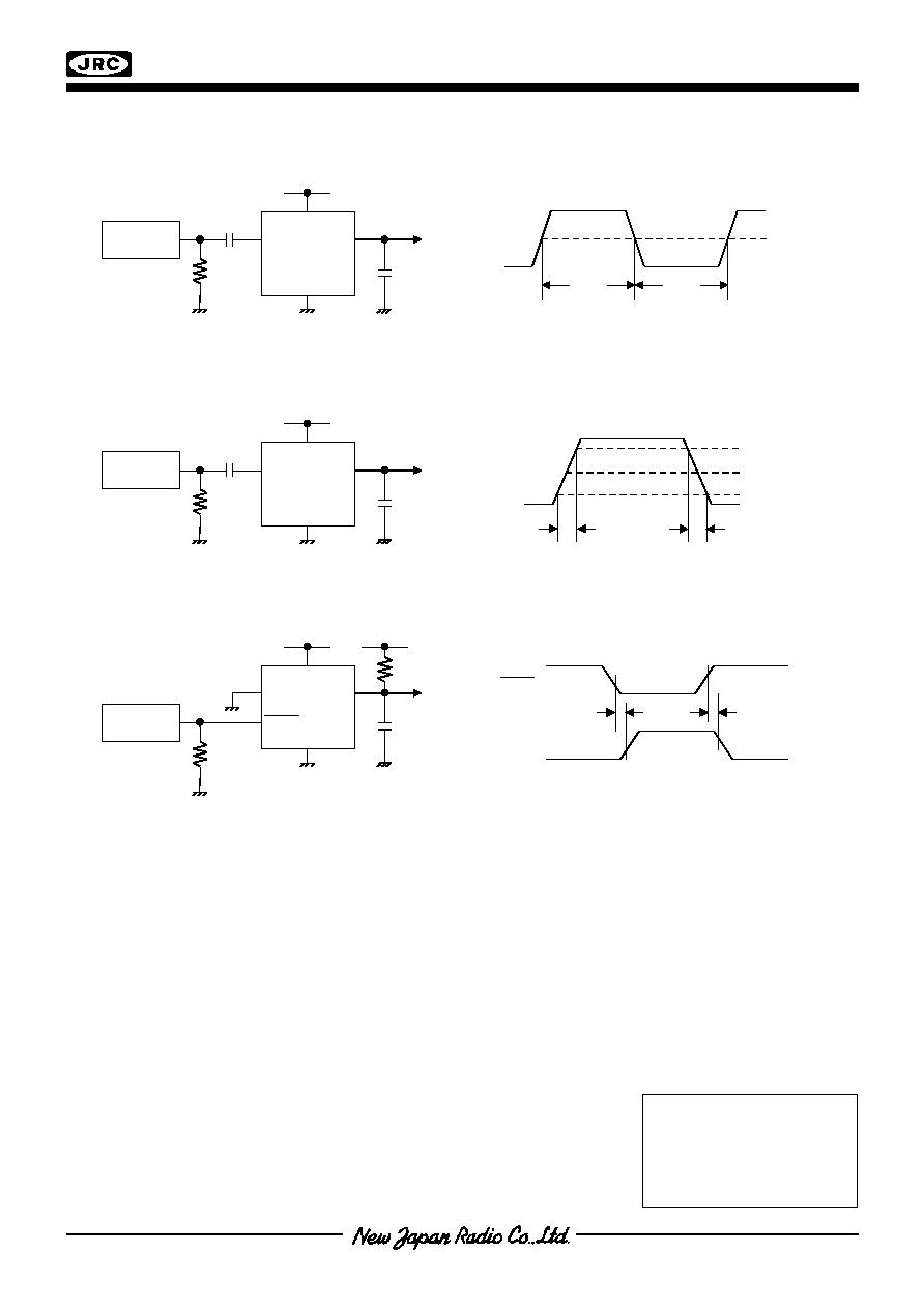
MEASURMENT CIRCUITS
(1)Output Signal Symmetry(C
L
=15pF, V
C
=1/2V
DD
)
(2)Output Signal Rise/Fall Time(C
L
=15pF, V
C
=1/2V
DD
)
(3)Output Disable/Enable Time(C
L
=15pF, R
UP
=10k
, V
C
=1/2V
DD
)
[CAUTION]
The specifications on this data book are only
given for information , without any guarantee
as regards either mistakes or omissions.
The application circuits in this data book are
described only to show representative usages
of the product and not intended for the
guarantee or permission of any right including
the industrial rights.
C
L
=15pF
Pulse
Generator
1000pF
50
V
DD
V
SS
XT
F
OUT
L
1/2V
DD
H
C
L
=15pF
Pulse
Generator
1000pF
50
V
DD
V
SS
XT
F
OUT
tr
tf
90%
10%
50%
R
UP
=10k
C
L
=15pF
Pulse
Generator
50
V
DD
V
SS
XT
F
OUT
CONT
T
PLZ
T
PZL
0.2V
DD
V
OL
0.8V
DD
V
OH
F
OUT
CONT