 | –≠–ª–µ–∫—Ç—Ä–æ–Ω–Ω—ã–π –∫–æ–º–ø–æ–Ω–µ–Ω—Ç: NJU6350 | –°–∫–∞—á–∞—Ç—å:  PDF PDF  ZIP ZIP |
NJU6350
SERIAL I/O REAL TIME CLOCK
s
GENERAL DESCRIPTION
The NJU6350 is a serial I/O Real Time Clock suitable for
4 bits micro-processor.
It contains quartz crystal oscillator, counter, shift register,
voltage regulator, voltage detector, and interface controller.
The NJU6350 required only 3-port of microprocessor for
data transfer, and the microprocessor can receive the data
at any time when the microprocessor requires.
The operating voltage is as wide as 2.0V to 5.5V,
consequently, the NJU6350 can count accurate time data
even if the back up period.
Furthermore, the long time back up is available as the
current consumption during the back up period is less than
2
µ
A.
s
FEATURES
q
Operating Voltage : 3.0V
±
20%
2.0V to 5.5V ( The clock operation )
q
Low operating current : 0.8
µ
A ( Typ. ) at 2.0V
2.0
µ
A ( Max. ) at 2.0V
q
BCD Counts of Seconds, Minutes, Hours, Days of Week,
Date, Month and Year
q
Required only 3-port ( DATA, CLK and CE )
q
Low Battery Detector ( Low voltage alarm signal output )
q
Automatic Leap Year Compensation : Up to AD 2099
q
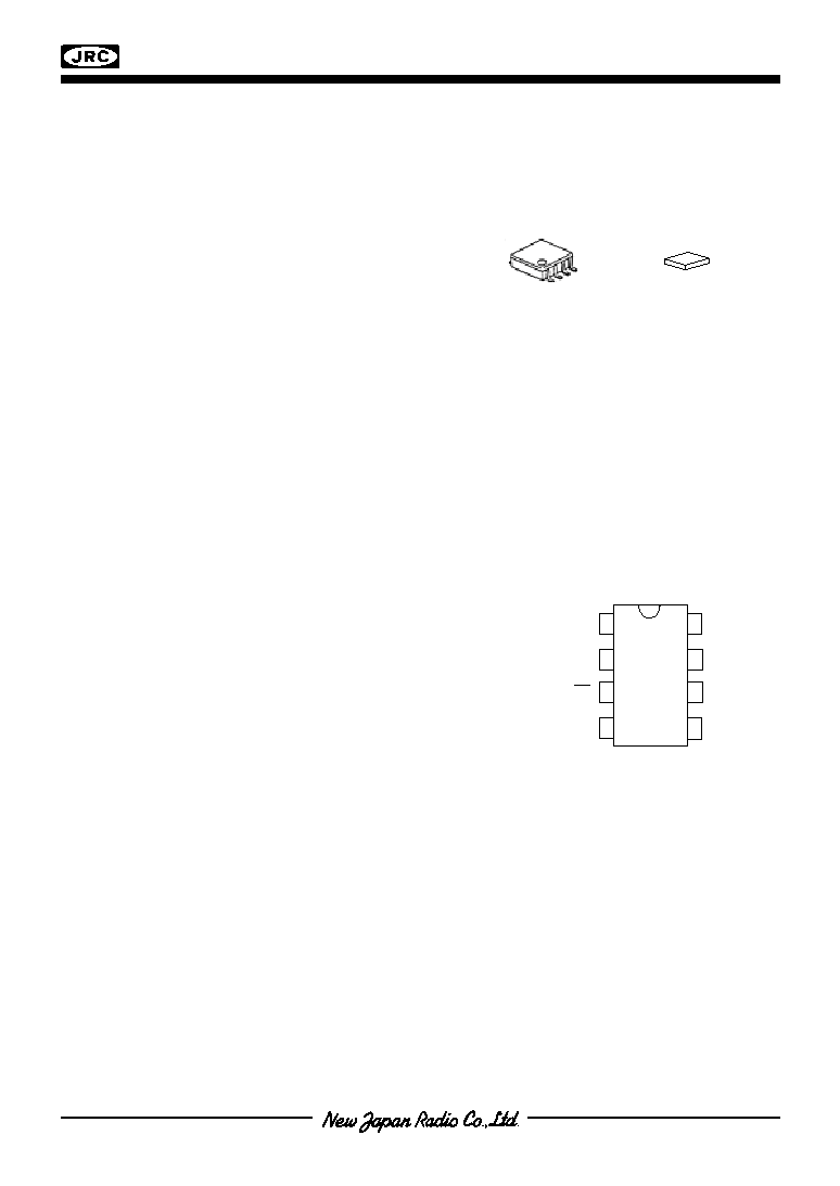
Package Outline : VSP 8 / Chip
q
C-MOS
Technology
s
PACKAGE OUTLINE
s
PIN CONFIGURATION
NJU6350R
NJU6350C
1
2
3
4
5
6
7
8
F
OUT
XT
XT
V
SS
X
DD
DATA
CLK
CE
NJU6350
s
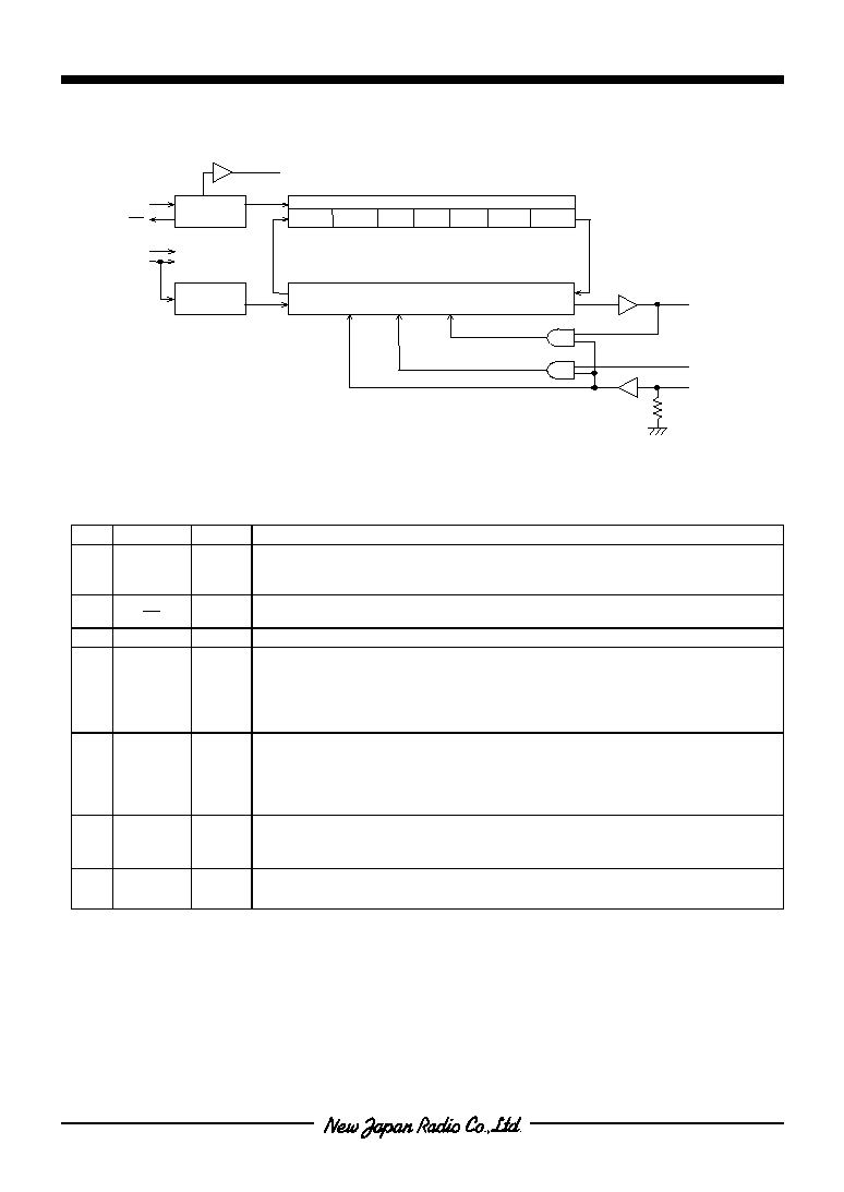
BLOCK DIAGRAM
s
TERMINAL DESCRIPTION
No.
SYMBOL
I/O
FUNCTION
1
Fout
O
Oscillator output terminal.
ON :It outputs oscillator signal , frequency 32.768kHz.
OFF :It is in high impedance status.
2
3
XT
XT
I
O
Quartz crystal connect terminal ( f = 32.768kHz ).
4
V
SS
Power
GND
5
CE
I
Chip enable terminal ( With pull-down resistor ).
" H " : Data input/output available
" L " : Data terminal is in high impedance status.
When the data input/output is executed consequently, the CE terminal should be
set to " L " level at the data transmission interval.
6
CLK
I
Clock terminal.
The Data Input/Output is synchronized by this clock. When the CE terminal is "L",
the data input is not available.
When the CE signal which is raising edge or falling edge, the CLK signal should
be fixed to " L ".
7
DATA
I/O
Serial timer data input/output terminal.
This terminal is switched to input or output by system control data. (Defult : input)
When the CE terminal is set to " L ", the data terminal is high impedance.
8
V
DD
Power
Power supply
The rising time of V
DD
should be less than 10mS.
Fout
XT
XT
V
SS
V
DD
Oscillator
Divider
Low Voltage
Detector
Timer Counter
sec.
min.
day
date
hour
month
year
Controller
DATA
CLK
CE
NJU6350
s
FUNCTIONAL DESCRIPTION
1. Timer and System control data format
The NJU6350 adopts BCD code consisting of 4 bits per digit.
The calendar function including the last date of each month and the leap year calculation is executed
automatically. The system control data operates Data I/O mode set, Oscillator output set and Test mode set.
The unused bit for the Timer and System control data is always set to " 0 ".
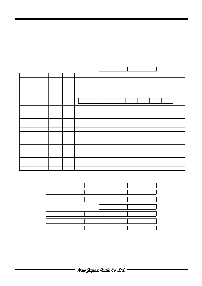
< System control data format >
MSB
LSB
System control data block
C2
C1
C0
RW
C2
C1
C0
RW
C o n t e n t s
Writing the data of oscillator output / test mode set
F = " 0 " : Oscilator output off (high impedance status)
F = " 1 " : Oscilator output on
T0 to 6:Test mode set ( Normaly all " 0 " )
MSB LSB
F
T6
T5
T4
T3
T2
T1
T0
0
0
0
1
0
0
1
1
Writing the data of " Year "
0
1
0
1
Writing the data of " Month "
0
1
1
1
Writing the data of " Date "
1
0
0
1
Writing the data of " Days of Week "
1
0
1
1
Writing the data of " Hour "
1
1
0
1
Writing the data of " Minute "
1
1
1
1
Writing the data of " Second "
0
0
1
0
Reading the data of " Year "
0
1
0
0
Reading the data of " Month "
0
1
1
0
Reading the data of " Date "
1
0
0
0
Reading the data of " Days of Week "
1
0
1
0
Reading the data of " our "
1
1
0
0
Reading the data of " Minute "
1
1
1
0
Reading the data of " Second "
0
0
0
0
nvalidity
< Timer data format >
MSB
LSB
Range
Second
0
S6
S5
S4
S3
S2
S1
S0
0
59
Minute
0
m6
m5
m4
m3
m2
m1
m0
0
59
Hour
0
0
H5
H4
H3
H2
H1
H0
0
23
Days of Week
DC
W2
W1
W0
1
7
Date
0
0
D5
D4
D3
D2
D1
D0
1
31
Month
0
0
0
M4
M3
M2
M1
M0
1
12
Year
Y7
Y6
Y5
Y4
Y3
Y2
Y1
Y0
0
99
Note1) The bit of " DC " in the " Days of Week " is a flag as the result of Low Voltage Detection. If the supply
voltage is reduced to the detection voltage level, then the flag of " DC " is set to "1" at the read operation,
and else the flag is always " 0 ".
(Note2) Only the data of Sec.., ..,Year as data of Timer and Calendar must be written to the NJU6350 why any
other data will be causes in malfunction of the timer counter.

NJU6350
2. Data writing operation
Data writing performs to set the system control data block ( 4 bits ) and the mode set data ( Oscillator output
control and Test mode set ) or the timer data block ( 8 bits, but only data of " Days of Week " is 4 bits ) to
NJU6350.
The CE terminal is set to " H ", and the data is written into the shift register in the NJU6350 from the DATA
terminal synchronizing with the rising edge of the clock signal input from the CLK terminal.
At first, System control data is written into NJU6350. The first 4 bits of them are effective. When the bit of
" RW " in System control data is " 1 ", the mode goes to writing. In the writing mode, the update of the timer is
stopped and the oscillator divider is cleared excepting for the Oscillation output set and Test mode set.
At second, Timer data is written into NJU6350. The last 8 bits of them are effective. ( In case of Days of week,
the last 4 bits are effective. )
The data order to write is LSB first.
The oscillator divider starts the operation when the CE signal is changed from " H " or " L ".
< Writing timer data >
In case of November
Input data
(Note3) In case of over than 12 bits data, valid data is the first 4 bits as System control data and the last 8 bits
as Timer data. ( In case of Days of week, it is the last 4 bits is effective. )
3. Data reading operation
Data reading performs to send the Timer data ( 8 bits, but only data of " Days of Week " is 4 bits )
corresponding the system control data from NJU6350 after the system control data ( 4 bits ) is set to NJU6350.
The CE terminal is set to " H ", and the System control data are written into the shift register in the NJU6350
from the DATA terminal synchronized with the rising edge of the clock signal input from the CLK terminal.
At first, System control data is written into NJU6350. The first 4 bits of them are effective. When the bit of
" RW " in System control data ( Except the " 0,0,0,0 " data. ) is " 0 " the mode goes to reading. When the falling
edge of the clock signal is input from the CLK terminal just after the recognition of reading mode, the DATA
terminal is changed from Input to Output. The first 8 bits of Read data is effective. ( In case of Days of week,
the first 4 bits is effective. ) After the falling edge of the CE terminal, the DATA terminal is changed from Output
to Input. The data order to read is LSB first.
(Note4) In case of counting the timer up during the data reading.
The difference between the read out data of timer and the actual timer data is sometimes occurred. ( The
difference range depend on condition. )
In case of " 99.12.31.Sat.23:59:59 " at the current time, the update is operated immediately after year but
" 99 " is read out, the data is the result of reading operation is " 99.1.1.Sun.0:0:0 " instead of the true data
" 00.1.1.Sun.0:0:0 ".
CLK
DATA
1
2
3
4
5
6
7
8
9
10
11
12
1
0
1
0
1
0
0
0
1
0
0
0
CE
RW
C0
C1
C2
M0
M1
M2
M3
M4
0
0
0

NJU6350
< Reading timer data >
In case of
( Note5 ) The first 8 bits of timer data are effective. (In case of Days of week, the first 4 bits are effective.)
4. Voltage Detect Function
The NJU6350 incorporates the low battery detector. If the supply voltage reduce to the detection level,
Detector check flag is " 1 " as warning code for the CPU. When power on reset or data writing operation, the
Detector check flag is set " 0 ". The low battery detector operates one time per 1 second.
5. Data Access
The NJU6350 can operate from 2.0V to 5.5V. However, the data access must operate in the range of
3V
±
20%.
6. Crystal Oscillator Circuit
The crystal oscillator circuit in the NJU6350 incorporates the capacitors. Therefore, it can operate with only
external crystal for 32.768kHz.
However, the external capacitors are required to get the matching between the incorporated oscillator and a
external crystal in accordance with the characteristics of crystal.
CLK
DATA
1
2
3
4
5
6
7
8
9
10
11
12
0
0
1
0
0
0
0
1
0
0
CE
1
0
RW
C0
C1
C2
M1
M2
M3
M4
0
0
M0
0
System control writing data
Timer reading data
The DATA terminal is changed over from Output to Input
Input data
The DATA terminal is changed over from Input to Output at the arrow.
Rf = 20M
(TYP)
32.768kHz
XT
XT
Cg = 31pF (TYP)
Ro = 320k
(TYP)
Cd = 18pF (TYP)
NJU6350
s
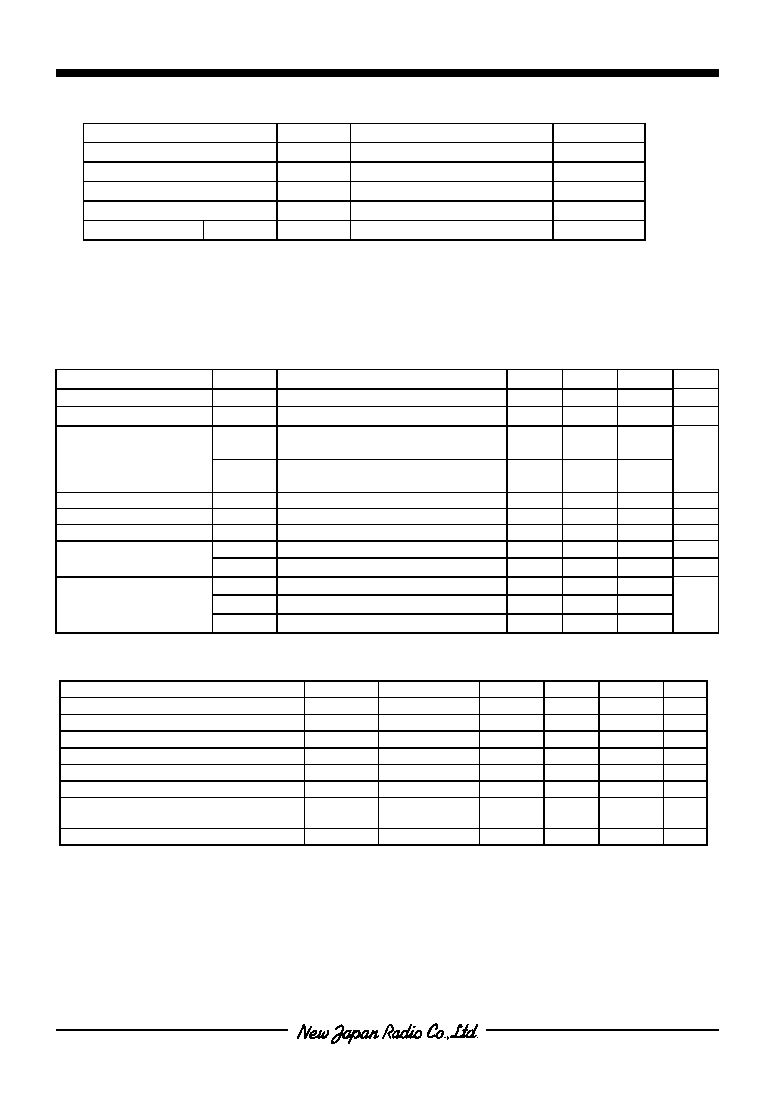
ABSOLUTE MAXIMUM RATINGS
P A R A M E T E R
SYMBOL
R A T I N G
UNIT
Supply Voltage
V
DD
-0.3 to +6.0
V
Input Voltage
VI
V
SS
-0.3 to V
DD
+0.3
V
Operating Temperature
Topr
-30 to +80
∞
C
Storage Temperature
Tstg
-40 to +125
∞
C
Power Dissipation
VSP
P
D
320
mW
Note1) Decoupling capacitor should be connected between V
DD
and V
SS
due to the stabilized operation of
the circuit.
s
ELECTRICAL CHARACTERISTICS
DC Characteristics ( Unless Otherwise Specified V
DD
=3V
±
20%, V
SS
=0V, Ta=25
∞
C )
P A R M E T E R
SYMBOL
C O N D I T O I N S
MIN.
TYP.
MAX.
UNIT
Operating Voltage
V
DD
2.0
3.6
V
Detecting Voltage
V
DET
1.3
1.6
1.9
V
I
DD1
Oscillation Output off, XT=32.768kHz
V
DD
=2.0V, CE=CLK=0V
0.8
2.0
Operating Current
I
DD2
Oscillation Output off, XT=32.768kHz
V
DD
=3.6V, CE=CLK=0V
0.8
2.0
µ
A
3-state Leakage Current
I
TSL
DATA Terminal ( CE=0V )
-2.0
2.0
µ
A
Input Leakage Current
I
IL
CLK Terminal
-1.0
1.0
µ
A
Input Current
I
IN
CE Terminal ( V
DD
=CE=3.6V )
12.0
µ
A
V
IH
CLK, CE, DATA Terminals
V
DD
X0.8
V
DD
µ
A
Input Voltage
V
IL
CLK, CE, DATA Terminals
V
SS
V
DD
x0.2
V
I
OH1
DATA Terminal ( V
DD
=2.4V, V
OH
=1.8V )
0.4
I
OH2
F
OUT
Terminal ( V
DD
=2.4V, V
OH
=1.8V )
1.0
Output Current
I
OL
DATA,F
OUT
Terminals ( V
DD
=2.4V, V
OL
=0.4V )
1.0
mA
AC Characteristics ( Unless Otherwise Specified V
DD
=3V
±
20%, V
SS
=0V, Ta=25
∞
C )
P A R A M E T E R
SYMBOL
CONDITIONS
MIN.
TYP.
MAX.
UNIT
CLK Pulse " H " Period
t
CWH
0.47
5000
µ
S
CLK Pulse " L " Period
t
CWL
0.47
5000
µ
S
CE Set-up Time Before CLK Rising
t
CS
470
nS
CE Hold Time After CLK Falling
t
CH
20
nS
DATA Set-up Time Before CLK Rising
t
WDS
100
nS
DATA Hold Time After CLK Rising
t
WDH
20
nS
DATA Delay Time CLK Falling
t
RDD
V
DD
=2.4V
CL=50pF
200
nS
Rise / Fall Time
t
RF
40
nS

NJU6350
s
TIMING CHART of Real Time Clock Block
1
2
3
4
5
6
7
8
9
10
System control data
CLK
DATA
11 12
1
2
3
4
5
6
7
8
9
10
11
12
(Write)
CE
DATA
(Read)
Timer data
System control data
Timer data
CE
CLK
DATA
t
CS
t
WDS
t
WDH
t
CWH
t
CWL
t
CH
t
RDD
CE
CLK
DATA
The DATA terminal is changed over from Input and Output.
NJU6350
s
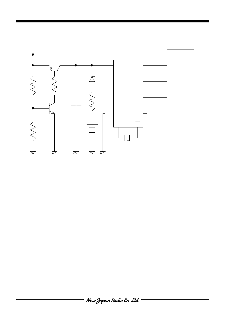
APPLICATION CIRCUIT
V
DD
V
SS
XT
XT
CE
CLK
DATA
F
OUT
VCC
32.768kHz
CPU
NJU6350

MEMO
[CAUTION]
The specifications on this databook are only
given for information , without any guarantee
as regards either mistakes or omissions. The
application circuits in this databook are
described only to show representative usages
of the product and not intended for the
guarantee or permission of any right including
the industrial rights.