2003/03/07 ( 1 / 6 )
NJU6363 Series
Low Operating Current Fundamental Quartz Crystal Oscillator
s
GENERAL DESCRIPTION
s
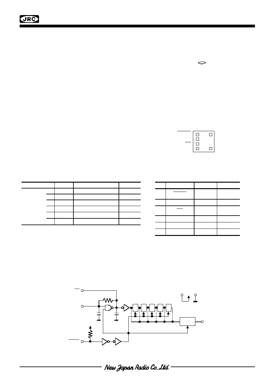
PACKAGE OUTLINE
The NJU6363 series is a C-MOS fundamental quartz crystal
oscillator that consists of an oscillation amplifier, 3-stage
divider and 3-state output buffer.
The 3-stage divider generates only one frequency selected
of f
0
,f
0
/2,f
0
/4 f
0
/8, f
0
/16 and f
0
/32 by internal circuits is output.
The oscillation amplifier is realized very low stand-by current
using NAND circuit.
The 3-state output buffer is C-MOS compatible.
s
FEATURES
s
PAD LOCATION
q
Low Operating Current
1mA @1.8V
q
Operating Voltage
1.5 to 3.6V
q
Maximum Oscillation Frequency
40MHz @1.5V
q
High Fan-out
I
OH
/I
OL
=1mA @1.8V
q
3-Stage Divider Maximum Divider f
0
/32
q
Oscillation Stop and Output Stand-by Function
q
3-State Output Buffer
q
Oscillation Capacitors Cg and Cg on-chip
q
Package Outline
Thin-Chip
q
C-MOS Technology
LINE-UP TABLE
COORDINATES
Starting Point:Chip Center Unit[um]
Chip
Size:0.7x0.75mm
Thin-Chip
Thickness(-D):200
�
20um
Pad
Size:90x90um
s
BLOCK DIAGRAM
Type No.
F
OUT
Internal
Connect Cg/Cd
A f
0
Connected
A
Line 8/9
B f
0
/2 Connected
B
Line 8/9
C f
0
/4
Connected C Line
8/9
D f
0
/8
Connected D Line
8/9
E f
0
/16 Connected
E
Line 8/9
NJU6363
F f
0
/32 Connected
F
Line 8/9
No
Pad Name
X
Y
1
CONT
-178 231
2
XT -178 77
3
XT
-178 -77
4
V
SS
-178
-231
5
F
OUT
206
-231
6
V
DD
206
231
NJU6363XC-D
CONT
XT
XT
Cg
Cd
Rf
2
/
1
2
/
1
2
/
1
2
/
1
2
/
1
A
B
C
D
E
F
BUFFER
STATE
3
-
OUT
F
DD
V
SS
V
Thin-Chip
CONT
XT
V
SS
F
OUT
XT
V
DD
2003/03/07 ( 2 / 6 )
NJU6363 Series
s
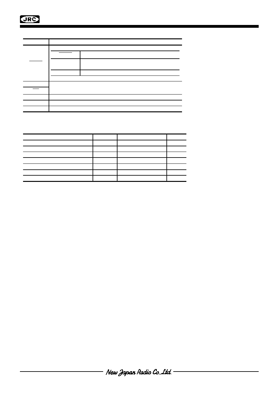
TREMINAL DESCRIPTION
SYMBOL FUNCTION
CONT
Oscillation and 3-state Output Buffer Control
CONT
F
OUT
H or OPEN
Output either one frequency selected of f
0
,
f
0
/2,f
0
/4,f
0
/8, f
0
/16 and f
0
/32 Note1)
L
Oscillation Stop and High impedance Output
XT
XT
Quartz Crystal Connecting Terminals
V
SS
V
SS
=0V
F
OUT
Frequency
Output
V
DD
V
DD
=1.8/2.5V/3.3V
Note1) Refer to the line-up table.
s
ABSOLUTE MAXIMUM RATINGS
(Ta=25�C)
PARAMETER SYMBOL
RATING UNIT
Supply Voltage
V
DD
-0.5
to
+7.0 V
Input Voltage
V
IN
V
SS
-0.5 to V
DD
+0.5 V
Output Voltage
V
O
-0.5
to
V
DD
+0.5 V
Input Current
I
IN
�
10
mA
Output Current
I
O
�
25
mA
Operating Temperature Range
Topr
-40 to +85
�C
Storage Temperature Range
Tstg
-55 to +125
�C
Note2) If the supply voltage(V
DD
) is less than 7.0V, the input voltage must not over the V
DD
level though 7.0V is
limit specified.
Note3) Decupling capacitor should be connected between V
DD
and V
SS
due to the stabilized operation for the
circuit.