2002/11/29 ( 1 / 6 )
NJU6376 Series
3rd. Over Tone Small Sized Quartz Crystal Oscillator
s
GENERAL DESCRIPTION
s
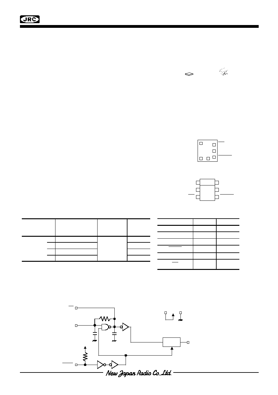
PACKAGE OUTLINE
The NJU6376 series is a C-MOS 3rd. over tone quartz
crystal oscillator that consists of an oscillation amplifier and
3-state output buffer.
The type numbers are classed into four versions G, H, J
and K according to their oscillation frequency range shown in
the line-up table.
The oscillation amplifier is realized very low stand-by
current using NAND circuit.
The 3-state output buffer is C-MOS compatible
Furthermore, the package is small-sized MTP-6.
s
FEATURES
s
PAD LOCATION/PIN CONFIGURATION
q
Operating Voltage
2.2 to 5.5V
q
Oscillation Frequency Range
(See Line-up Table)
q
Low Operating Current
q
High Fan-out
I
OH
/I
OL
=4mA @2.5V
q
Oscillation Stop and Output Stand-by Function
q
3-State Output Buffer
q
Oscillation Capacitors Cg and Cd on-chip
q
Package Outline
Chip/MTP-6
q
C-MOS Technology
s
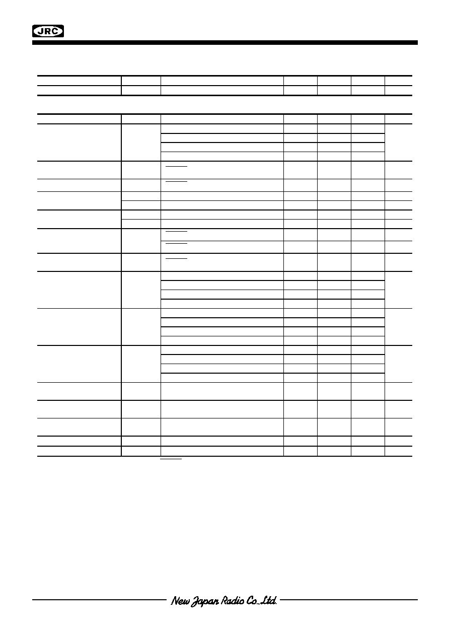
LINE-UP TABLE
s
COORDINATION
s
BLOCK DIAGRAM
Type No.
Recommended
Oscillation
Frequency Range
Output
Frequency
Cg/Cd
G
30 to 40MHz
18/18pF
H
40 to 50MHz
16/16pF
J
50 to 60MHz
11/11pF
NJU6376
K
60 to 75MHz
f
0
10/10pF
Pad Name
X
Y
F
OUT
-220
245
V
SS
-205
-230
XT 13
-230
CONT
205 -191
V
DD
205
0
XT
205 191
Starting Point:Chip Center Unit[um]
Chip Size: 0.70x0.75mm
Thin-Chip Thickness(-C):260
�
20um
Pad Size:90x90um
NJU6376XC-C NJU6376XF1
F
OUT
V
SS
XT
V
DD
XT
CONT
1
2
3
6
5
4
MTP-6
Thin-Chip
CONT
XT
V
SS
F
OUT
XT
V
DD
CONT
XT
XT
Cg
Cd
Rf
BUFFER
STATE
3
-
OUT
F
DD
V
SS
V
2002/11/29 ( 2 / 6 )
NJU6376 Series
s
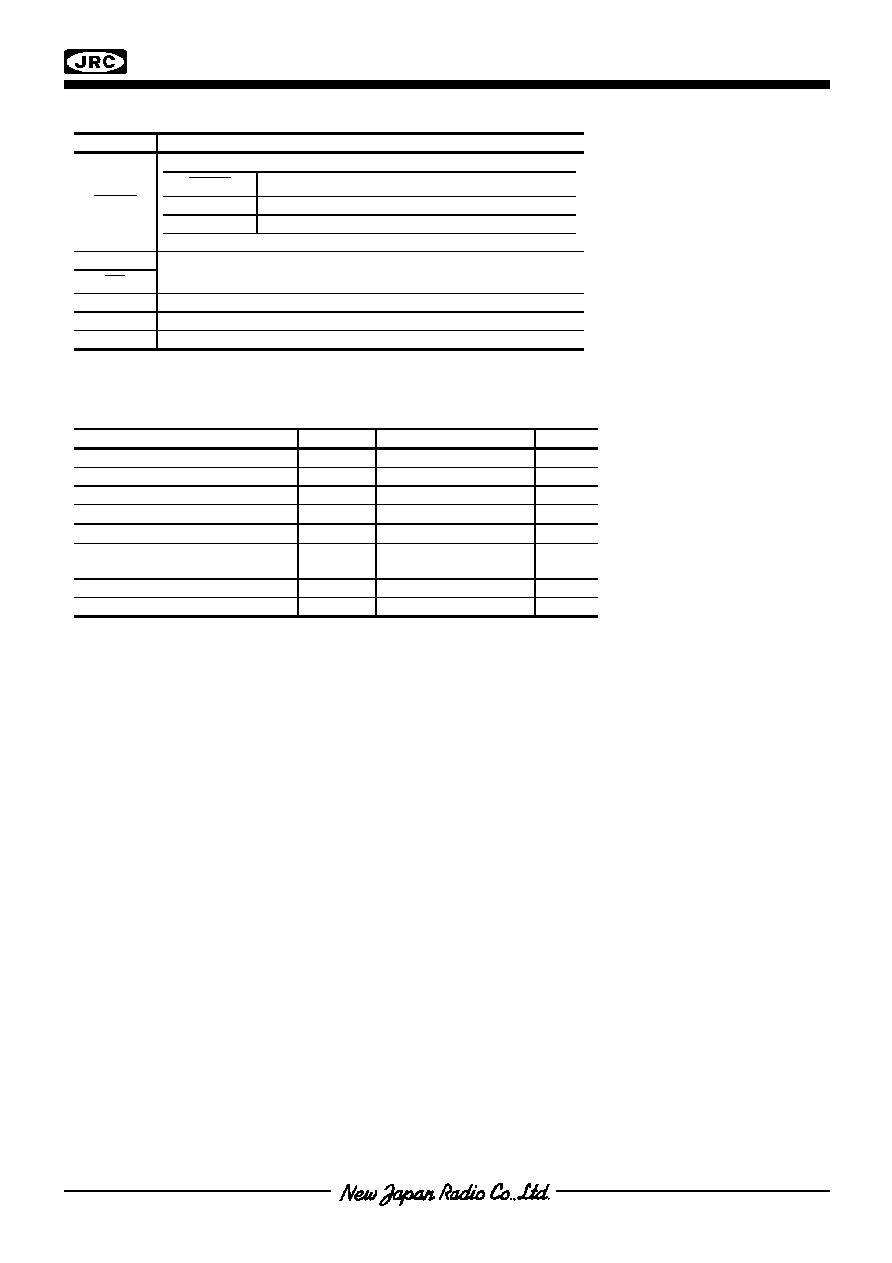
TREMINAL DESCRIPTION
SYMBOL FUNCTION
CONT
Oscillation and 3-state Output Buffer Control
CONT
F
OUT
H or OPEN Output frequency f
0
Note1)
L
Oscillation Stop and High impedance Output
XT
XT
Quartz Crystal Connecting Terminals
V
SS
V
SS
=0V
F
OUT
Frequency
Output
V
DD
V
DD
=2.5V/3.0V/5.0V
Note1) Refer to the line-up table.
s
ABSOLUTE MAXIMUM RATINGS
(Ta=25�C)
PARAMETER SYMBOL
RATING UNIT
Supply Voltage
V
DD
-0.5
to
+7.0 V
Input Voltage
V
IN
V
SS
-0.5 to V
DD
+0.5 V
Output Voltage
V
O
-0.5
to
V
DD
+0.5 V
Input Current
I
IN
�
10
mA
Output Current
I
O
�
25
mA
Power Dissipation
Note4)
P
D
200(MTP-6)
mW
Operating Temperature Range
Topr
-40 to +85
�C
Storage Temperature Range
Tstg
-55 to +125
�C
Note2) If the supply voltage(V
DD
) is less than 7.0V, the input voltage must not over the V
DD
level though 7.0V is
limit specified.
Note3) Decupling capacitor should be connected between V
DD
and V
SS
due to the stabilized operation for the
circuit.
Note4) The power dissipation is the maximum value at only the package.