2003/03/07 ( 1 /
4
)
NJU6396
3rd. Over Tone Quartz Crystal Oscillator for 166MHz
s
GENERAL DESCRIPTION
s
PACKAGE OUTLINE
The NJU6396 is a C-MOS IC for XOs, and can oscillate up
to 166MHz maximum at very low operating voltage.
High Fan-out is gained from low operating voltage with
3-state output buffer and the oscillation amplifier that is
realized very low stand-by current using NAND circuit.
Furthermore, not using PLL, the electrical character shows
a very low jitter.
The NJU6396 is suitable for mobile, optical communications
(included WDM system) and not to mention previous
applications; Computer & Peripherals, telecommunications,
LAN/WAN, Wireless and so on.
s
FEATURES
s
PAD LACATION
q
Operating Voltage
2.7 to 3.6V
q
Maximum Oscillation Frequency 166MHz
q
High Fan-out
I
OH
/I
OL
=8mA @3.3V
q
Oscillation Stop and Output Stand-by Function
q
3-State Output Buffer
q
Oscillation Capacitors Cg and Cg on-chip
q
Package Outline
q
C-MOS Technology
Thin-Chip
s
PAD CONFIGURATION
Starting Point:Chip Center Unit[um]
Chip
Size:0.7x0.75mm
Thin-Chip
Thickness:200
�
20um
Pad
Size:90x90um
s
BLOCK DIAGRAM
No
Pad Name
X
Y
1
CONT -178 231
2
XT -178 77
3
XT -178
-77
4
V
SS
-178
-231
5
F
OUT
206 -231
8
V
DD
206 231
NJU6396C-D
CONT
XT
XT
Cg
Cd
Rf
BUFFER
STATE
3
-
OUT
F
DD
V
SS
V
Thin-Chip
CONT
XT
V
SS
F
OUT
XT
V
DD
2003/03/07 ( 2 /
4
)
NJU6396
s
TREMINAL DESCRIPTION
SYMBOL FUNCTION
CONT
Oscillation and 3-state Output Buffer Control
CONT
F
OUT
H or OPEN Output frequency f
0
L
Oscillation Stop and High impedance Output
XT
XT
Quartz Crystal Connecting Terminals
V
SS
V
SS
=0V
F
OUT
Frequency
Output
V
DD
V
DD
=3.3V
s
ABSOLUTE MAXIMUM RATINGS
(Ta=25
�
C)
PARAMETER SYMBOL
RATING UNIT
Supply Voltage
V
DD
-0.5
to
+7.0 V
Input Voltage
V
IN
V
SS
-0.5 to V
DD
+0.5 V
Output Voltage
V
O
-0.5
to
V
DD
+0.5 V
Input Current
I
IN
�
10
mA
Output Current
I
O
�
25
mA
Operating Temperature Range
Topr
-40 to +85
�
C
Storage Temperature Range
Tstg
-55 to +125
�
C
Note1) If the supply voltage(V
DD
) is less than 7.0V, the input voltage do not over the V
DD
level.
Note2) Decupling capacitor should be connected between V
DD
and V
SS
due to the stabilized operation for the
circuit.
2003/03/07 ( 4 /
4
)
NJU6396
s
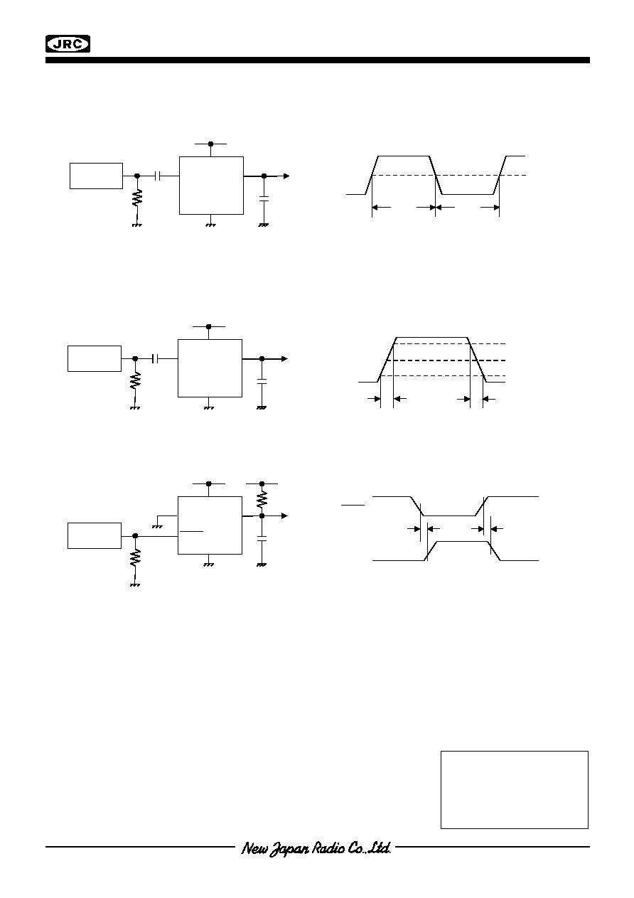
MEASURMENT CIRCUITS
(1)Output Signal Symmetry(C
L
=15pF)
(2)Output Signal Rise/Fall Time(C
L
=15pF)
(3)Output Disable/Enable Time(C
L
=15pF,R
UP
=10k
)
[CAUTION]
The specifications on this data book are only
given for information , without any guarantee
as regards either mistakes or omissions.
The application circuits in this data book are
described only to show representative usages
of the product and not intended for the
guarantee or permission of any right including
the industrial rights.
C
L
=15pF
Pulse
Generator
1000pF
50
V
DD
V
SS
XT
F
OUT
L
1/2V
DD
H
C
L
=15pF
Pulse
Generator
1000pF
50
V
DD
V
SS
XT
F
OUT
tr
tf
90%
10%
50%
R
UP
=10k
C
L
=15pF
Pulse
Generator
50
V
DD
V
SS
XT
F
OUT
CONT
T
PLZ
T
PZL
0.2V
DD
V
OL
0.8V
DD
V
OH
F
OUT
CONT