
- 1 -
NJU6533
Ver.2004-03-05
1/3, 1/4 Duty LCD Driver
!
GENERAL DESCRIPTION
NJU6533 is a 1/3 or 1/4 duty segment type LCD driver.
It incorporates 4 common driver circuits and 32 segment driver
circuits. NJU6533 can drive maximum 96 segments in 1/3 duty
ratio and maximum 128 segments in 1/4 duty ratio.
Controlled by MPU, NJU6533 can be used in many LCD
applications
!
FEATURES
#
LCD driving circuit
:Max. 32outputs (4 outputs as for general purpose ports)
#
Programmable Duty Ratio
1/3 duty ratio
:Driving max. 96 segments
1/4 duty ratio
:Driving max. 128 segments
#
Programmable Bias Ratio :1/2, 1/3 bias ratio
#
Serial Data Transfer
:Shift clock max. 2MHz
#
Built-in Oscillator
:
CR oscillation with external resistor, or external oscillation signal input.
#
Display OFF
:INHb pin
#
Operating Voltage
:3V / 5.0V
#
C-MOS Technology
:
P-Sub
#
Package Outline
:QFN48
!
BLOCK DIAGRAM
!
PACKAGE OUTLINE
NJU6533KQ1
COM1
V
LCD
V
1
V
2
V
SS
V
DD
INHb
OSC2
Oscillator
COM4
CSb
SCK
SI
Segment Drivers /General Purpose Output Ports
SEG1 SEG8
SEG9 SEG16 SEG17 SEG24 SEG25 SEG32/P4
Decoder
Data Latch Circuit
Command Register
Display Data Register
COM
Drivers
OSC1
RSTb
Power ON Reset Circuit
PRELIMINARY

- 2 -
NJU6533
Ver.2004-03-05
!
PIN CONFIGURATION
!
TERMINAL DISCRIPTION
No. Pad
Name
Function
46 V
DD
Power supply: 3V /5V
37 V
LCD
LCD driving voltage
V
LCD
V
1
V
2
V
SS
, V
LCD
V
DD
38,
39
V
1
,
V
2
Bias
At 1/3 bias ratio, keep V
1
- V
2
open
At 1/2 bias ratio, short V
1
- V
2
40 V
SS
GND
V
SS
=0V
41 INHb
Display OFF
When INHb is "H", display is ON, and when INHb is "L", display is off.
When INHb is "L", all segment and common drivers output V
SS,
and the
oscillator stop operation. But, if at the same time RSTb="L", the oscillator
functions and all segment and common drivers output V
SS
42 RSTb
Reset
When RSTb is "L", command register and latch circuit is reset
43 CSb
Chip select
When CSb is "L", data can be read in.
44
SI
Serial data input (8 bit=1word)
45 SCK
Serial
clock
47,
48
OSC1,
OSC2
External resistor connection pin for CR oscillation, or external clock input pin.
When external clock is used, input the signal to OSC1 and keep OSC2 open.
1~4
COM1 ~ COM4
Common driver outputs
5~32
SEG1 ~ SEG28
Segment driver outputs
33~36
SEG29/P1 ~
SEG32 /P4
Segment driver outputs/general purpose output ports
These 4 pins can be used as segment driver outputs or general purpose output
ports by setting Command Register.
When selected as general purpose ports, data can be outputted via these ports
during COM1 timing.
According to transferred data, "H"=V
DD
or "L"=V
SS
will be outputted.
37
1
2
3
4
5
6
7
8
10
11
12
27
26
25
30
29
28
33
32
31
36
35
34
38
39
40
41
42
43
44
45
46
47
48
24
23
22
21
20
19
18
17
16
15
14
13
COM
1
SEG9
NJU6533
COM
2
COM
3
COM
4
SEG
1
SEG
2
SEG
3
SEG
4
SEG
5
SEG
6
SEG
7
SEG
8
SEG
2
1
SEG10
SEG11
SEG12
SEG13
SEG14
SEG15
SEG16
SEG17
SEG18
SEG19
SEG20
OSC2
OSC1
V
DD
SCK
SI
CSb
RSTb
INHb
V
SS
V
2
V
1
V
LCD
SEG
2
2
SEG
2
3
SEG
2
4
SEG
2
5
SEG
2
6
SEG
2
7
SEG
2
8
S
E
G
29
/
P
1
S
E
G
30
/
P
2
S
E
G
31
/
P
3
S
E
G
32
/
P
4
9

- 3 -
NJU6533
Ver.2004-03-05
!
FUNCTION DESCRIPTION
(1) Block Function
�
Oscillator
The oscillator includes a built-in capacitor and an external resistor. It generates clock signal for LCD driving. When
use external clock, input the clock signal to OSC1 and keep OSC2 open.
�
Decoder
Input serial data is decoded and sent to the appropriate block.
�
Command Register
Command data is written to this 8 bits command register to control NJU6533 operation.
�
Display Data Register
Data is written to this 8 bits register as display data.
�
Latch Circuit
Data stored in display data register is assigned to the corresponding SEG/port.
�
Segment Driver/General Purpose Ports
Basing on display data, segment drivers output LCD SEG driving signal.
And, SEG29/P1 ~ SEG32/P4 pins can be selected as segment driver output or general-purpose ports by instruction.
�
Common Driver
Common drivers output LCD COM driving signal.
�
Power On Reset
When power is on, NJU6533 is automatically initialized. And if RSTb="L", NJU6533 is reset too.
- 4 -
NJU6533
Ver.2004-03-05
!
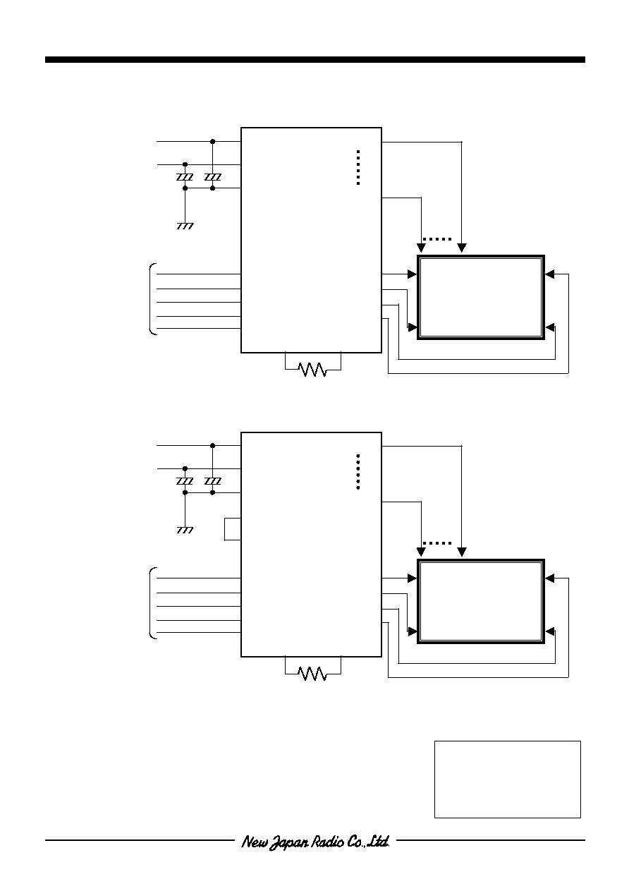
APPLICATION CIRCUIT
�
1/4 duty, 1/3 bias
�
1/4 duty, 1/2 bias
Note)
Because display data is not yet stable just after V
DD
on, if LCD panel is turned on, unexpected pattern will be
displayed, therefore, keep INHb terminal to "L" level until data transfer from MPU is over.
[CAUTION]
The specifications on this databook are only
given for information , without any guarantee
as regards either mistakes or omissions. The
application circuits in this databook are
described only to show representative usages
of the product and not intended for the
guarantee or permission of any right including
the industrial rights.
V
LCD
V
DD
V
SS
V
1
V
2
RSTb
INHb
CSb
SCK
SI
NJU6533
SEG1
SEG34/P4
COM1
COM2
COM3
COM4
+ +
V
LCD
V
DD
From MPU
LCD Panel
OSC1
OSC2
V
LCD
V
DD
V
SS
V
1
V
2
RSTb
INHb
CSb
SCK
SI
NJU6533
SEG1
SEG34/P4
COM1
COM2
COM3
COM4
+ +
V
LCD
V
DD
From MPU
LCD Panel
OSC1
OSC2