NJU6678V
NJU6678V
104-common x 132-segment
104-common x 132-segment
BIT MAP LCD DRIVER
BIT MAP LCD DRIVER
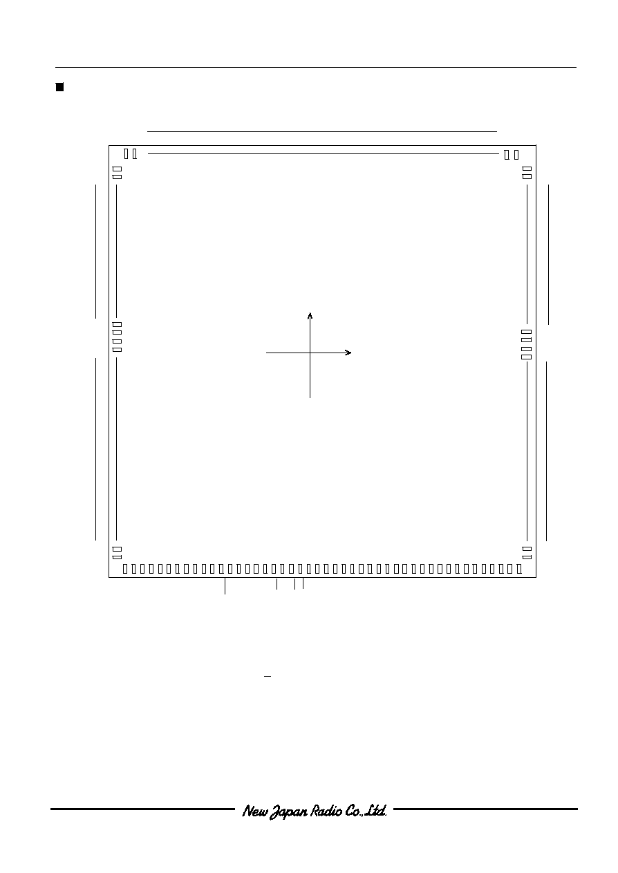
PACKAGE OUTLINE
PACKAGE OUTLINE
NJU6678VCL
NJU6678VCL
GENERAL DESCRIPTION
GENERAL DESCRIPTION
FEATURES
FEATURES
The
The
NJU6678V
NJU6678V is a 104-common x 132-segment bit map LCD driver to
is a 104-common x 132-segment bit map LCD driver to
display graphics or characters.
display graphics or characters.
It contains 21,120 bits display data RAM, microprocessor interface cir-
It contains 21,120 bits display data RAM, microprocessor interface cir-
cuits, instruction decoder, and common and segment drivers.
cuits, instruction decoder, and common and segment drivers.
An image data from CPU through the serial or 8-bit parallel interface are
An image data from CPU through the serial or 8-bit parallel interface are
stored into the 21,120 bits internal display data RAM and are displayed
stored into the 21,120 bits internal display data RAM and are displayed
on the LCD panel through the commons and segments drivers.
on the LCD panel through the commons and segments drivers.
The
The
NJU6678V
NJU6678V displays 104 x 132 dots graphics or 8-character 6-line
displays 104 x 132 dots graphics or 8-character 6-line
by 16 x 16 dots character.
by 16 x 16 dots character.
The
The
NJU6678V
NJU6678V contains a built-in OSC circuit for reducing external com-
contains a built-in OSC circuit for reducing external com-
ponents. And it features Partial Display Function containing selectable
ponents. And it features Partial Display Function containing selectable
active display block(s) (two blocks max.) and optimizing the duty cycle
active display block(s) (two blocks max.) and optimizing the duty cycle
ratio. This function dramatically reduces the operating current, setting
ratio. This function dramatically reduces the operating current, setting
the optimum boosted voltage combined with a programmable voltage
the optimum boosted voltage combined with a programmable voltage
booster circuit and an electrical variable resister. As result, it reduces
booster circuit and an electrical variable resister. As result, it reduces
the operating current.
the operating current.
The operating voltage from 2.5V to 3.3V and low operating current are
The operating voltage from 2.5V to 3.3V and low operating current are
suitable for small size battery operation items.
suitable for small size battery operation items.
Direct Correspondence of Display Data RAM to LCD Pixel
Direct Correspondence of Display Data RAM to LCD Pixel
Display Data RAM - 21,120 bits ;(1.5 times over than display size)
Display Data RAM - 21,120 bits ;(1.5 times over than display size)
LCD drivers - 104-common and 132-segment
LCD drivers - 104-common and 132-segment
Direct connection to 8-bit Microprocessor interface for both of 68 and 80 type MPU
Direct connection to 8-bit Microprocessor interface for both of 68 and 80 type MPU
Serial Interface
Serial Interface
Partial Display Function Two limited active display blocks setting. Duty ratio set automatically.
Partial Display Function Two limited active display blocks setting. Duty ratio set automatically...
Easy Vertical Scroll by setting the start line address of over size display data RAM
Easy Vertical Scroll by setting the start line address of over size display data RAM
Programmable Bias selection ; 1/4,1/5,1/6,1/7,1/8,1/9,1/10,1/11 bias
Programmable Bias selection ; 1/4,1/5,1/6,1/7,1/8,1/9,1/10,1/11 bias
Common Driver Order Assignment by mask option
Common Driver Order Assignment by mask option
Version
Version
C
C
0
0
to C
to C
103
103
(Pin name)
(Pin name)
NJU6678VA
NJU6678VA Com
Com
0
0
to Com
to Com
103
103
NJU6678VB
NJU6678VB Com
Com
103
103
to Com
to Com
0
0
Useful Instruction Sets
Useful Instruction Sets
Display ON/OFF Cont, Display Start Line Set, Page Address Set, Column Address Set, Status Read,
Display ON/OFF Cont, Display Start Line Set, Page Address Set, Column Address Set, Status Read,
Display Data Read/Write, Inverse Display, All On/Off, Partial Display, Bias Select, n-Line Inverse,
Display Data Read/Write, Inverse Display, All On/Off, Partial Display, Bias Select, n-Line Inverse,
Voltage Booster Circuits Multiple Select(Maximum 5-time), Read Modify Write, Power Saving, ADC Select, etc.
Voltage Booster Circuits Multiple Select(Maximum 5-time), Read Modify Write, Power Saving, ADC Select, etc.
Power Supply Circuits for LCD; Programmable Voltage Booster Circuits(5-time Maximum,
Power Supply Circuits for LCD; Programmable Voltage Booster Circuits(5-time Maximum, Voltage boosting
Voltage boosting
polarity:Negative voltage(V
polarity:Negative voltage(V
DD
DD
Common)
Common)),Regulator, Voltage Follower (x 4)
),Regulator, Voltage Follower (x 4)
Precision Electrical Variable Resistance
Precision Electrical Variable Resistance
Low Power Consumption
Low Power Consumption
Operating Voltage
Operating Voltage
--- 2.5V to 3.3V
--- 2.5V to 3.3V
LCD Driving Voltage
LCD Driving Voltage --- 6.0V to 17V
--- 6.0V to 17V
Package Outline
Package Outline
--- TCP / Bumped Chip
--- TCP / Bumped Chip
C-MOS Technology (
C-MOS Technology (Substrate:N)
Substrate:N)
2003
2003
Ver.4.9
Ver.4.9