NJU6680
- 1 -
Ver.2003-04-08
128-common x 128-segment 4-level Gray Scale
BITMAP LCD DRIVER
GENERAL DESCRIPTION
The NJU6680 is a 128-common x 128-segment 4-level
gray scale bit map LCD driver to display graphics or
characters.
It contains 32,768-bit display data RAM, microprocessor
interface circuits, instruction decoder, and common and
segment drivers.
An image data from CPU through the serial or 8-bit
parallel interface are stored into the 32,768-bit internal
display data RAM and are displayed on the LCD panel
through the commons and segments drivers.
The NJU6680 features 4-level gray scale display
function creating 4 types of gray scale (white / light gray /
dark gray / black) and black & white display function.
The NJU6680 contains a built-in OSC circuit for
reducing external components. And it features Partial
Display Function containing selectable active display
block and optimizing the duty cycle ratio. This function
dramatically reduces the operating current, setting the
optimum boosted voltage combined with a programmable
voltage booster circuit and an electrical variable resistor.
As result, it reduces the operating current.
The operating voltage from 2.2V to 3.6V and low
operating current are suitable for small size battery
operation items.
FEATURES
Direct Correspondence of Display Data RAM to LCD Pixel
Display Method � 4-level Gray Scale / Black & White
Display Data RAM � 32,768 bits ;( 128-Com x 128-Seg) x 2bit
LCD drivers � 128-common and 128-segment
Direct connection to 8-bit Microprocessor interface for both of 68 and 80 type MPU
Serial Interface (SI, SCL, RS, CS)
Partial Display Function
Easy Vertical Scroll by setting the start line address of over size display data RAM
Programmable Bias ratio selection ; 1/5, 1/6, 1/7, 1/8, 1/9, 1/10, 1/11, 1/12 bias
Useful Instruction Sets
Status read, Display data write, Column address set, Page address set, Initial display line set, Initial COM
0
line set, Display ON/OFF, Entire display ON/OFF, Reverse display ON/OFF, N-line inversion set, N-line
inversion OFF, ADC select, COM scan direction select, Internal resistor ratio set, Power control set, Partial
display duty set, LCD bias set, Boost level set, Contrast level set, Power save mode ON, Power save mode
OFF, Internal oscillator ON, Display data length set, Reset, FRC & PWM set, Grey scale mode set Display
mode set.
Power Supply Circuit for LCD; Programmable Booster Circuits (6 times maximum, Voltage boosting polarity :
Positive Voltage (V
SS
Common), Voltage Regulator, Voltage Follower (x 4))
Precision Electrical Variable Resistance (64 Step)
Low Operating Current
I
OUT1
=400
�
A (TYP.)
Operating Voltage
2.2 to 3.6 V
LCD Driving Voltage
6.0 to 18.0V
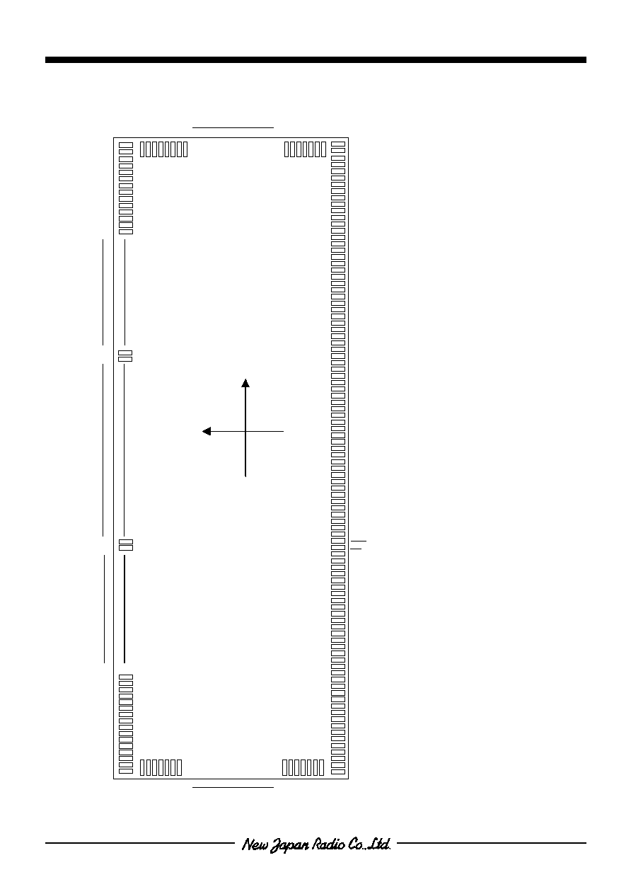
Package Outline
Bumped Chip
C-MOS Technology ( Substrate : P )
NJU6680CL
PACKAGE OUTLINE