
PRELIMINARY
1
NJU7043
Input/Output Full-Swing
High Output Current Dual C-MOS Operational Amplifier
s
GENERAL DESCRIPTION
s
PACKAGE OUTLINE
The NJU7043 is a dual C-MOS operational amplifier
permitting a full-swing input and output in full-swing under
high load.
Based on C-MOS technology, there are excellent features
such as high output current, low current consumption, low
operating voltage.
s
FEATURES
q
Oprating Voltage
V
DD
=1.8 to 5.0V
q
Input/Output Full-Swing
q
High Output Current
I
sourse
>40mA typ.at V
o
I
sink
<-40mA typ. at V
o
q
Input Offset Voltage
V
IO
=7mV max.
q
Wide Input Common Mode Voltage Range V
SS
to V
DD
q
Operating Current
I
DD
=700µA typ.
q
High Input Impedance
1T
typ.
q
Low Input Bias Current
I
IB
=1pA typ.
q
Ground Sensing
q
Tiny Package
DIP8, DMP8, SSOP8, TVSP8
s
PIN CONFIGURATION
NJU7043D
NJU7043M
NJU7043V
NJU7043RB1
1
2
3
5
4
-
+
+
-
7
6
8
PIN FUNCTION
1.OUTPUT1
2.-INPUT1
3.+INPUT1
4.V
SS
5.+INPUT2
6.-INPUT2
7.OUTPUT2
8.V
DD
PRELIMINARY
2
NJU7043
s
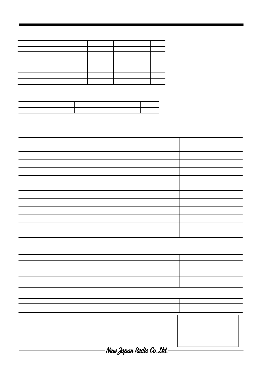
ABSOLUTE MAXIMUM RATINGS
(Ta=25
∞
C)
(Note 1)
If the supply voltage (V
DD
) is less
than 5.5V, the input voltage must not
over the V
DD
level through 5.5V is limit
specified.
(Note 2)
Decoupling capacitor should be
connected between V
DD
and V
SS
due
to the stabilized operation for the
circuit.
s
RECOMMENDED OPERATION CONDITION
(Ta=25
∞
C)
s
ELECTRICAL CHARACTERISTICS
q
DC CHARACTERISTICS
(V
DD
=3.0V,Ta=25
∞
C)
PARAMETER SYMBOL
TEST
CONDITION
MIN
TYP
MAX
UNIT
Operating Current
I
D D
No Signal, Dual Circuits
-
600 1,000 µA
Input Offset Voltage
V
I O
- -
7
mV
Input Bias Current
I
B
- 1 - pA
Input Offset Current
I
I O
- 1 - pA
Voltage Gain
A
V
R
L
=10k
70 90 - dB
Common Mode Rejection Ratio
CMR
0
V
CM
1.5V,1.5
V
CM
3.0V(Note)
45 60 - dB
Supply Voltage Rejection Ratio
SVR
2.4V
V
DD
5.0V, V
CM
=V
DD
/2
70 80 - dB
H Level Output Voltage 1
V
O H 1
R
L
=10k
2.95
- - V
L Level Output Voltage 1
V
O L 1
R
L
=10k
- -
0.05
V
H Level Output Voltage 2
V
O H 2
R
L
=600
2.90
- - V
L Level Output Voltage 2
V
O L 2
R
L
=600
- -
0.10
V
Input Common Mode Voltage Range
V
I C M
CMR>45dB
0 - 3 V
(Note) CMR is represented by either CMR+ or CMR- which has lower value.
CMR+ is measured with 1.5V
V
CM
3V and CMR- is measured with 0V
V
CM
1.5V .
q
AC CHARACTERISTICS
(V
DD
=3.0V, Ta=25
∞
C)
PARAMETER SYMBOL
TEST
CONDITION
MIN
TYP
MAX
UNIT
Unity Gain Bandwidth
GB
R
L
=10k
- 0.8 - MHz
Total Harmonic Distortion
T HD
f=1kHz , Vin=1Vpp
, A
v
=0dB -
0.05
-
%
Equivalent Input Noise Voltage
e
n
f=1kHz
- 40 -
nV/
Hz
q
TRANSIENT CHARACTERISTICS
(V
DD
=3.0V, Ta=25
∞
C)
PARAMETER SYMBOL
TEST
CONDITION
MIN
TYP
MAX
UNIT
Slew Rate
SR
R
L
=10k
- 0.7 - V/µs
PARAMETER SYMBOL
RATING
UNIT
Supply Voltage
V
DD
5.5
V
Power Dissipation
P
D
500 (DIP8)
250 (SSOP8)
300 (DMP8)
320 (TVSP8)
mW
Operating Temperature Range
Topr
-40 to +85
∞
C
Storage Temperature Range
Tstg
-55 to +125
∞
C
PARAMETER SYMBOL RATING UNIT
Supply Voltage
V
DD
1.8 to 5.0
V
[CAUTION]
The specifications on this databook are only
given for information , without any guarantee
as regards either mistakes or omissions. The
application circuits in this databook are
described only to show representative usages
of the product and not intended for the
guarantee or permission of any right including
the industrial rights.