
NJU3555
NJU3555
NJU8714
- 1 -
Ver.2004-05-21
STEREO BTL OUTPUTS SWITCHING DRIVER
FOR Class D AMPLIFIER
GENERAL DESCRIPTION
The
NJU8714
is a stereo BTL outputs switching driver
for class D amplifier. It receives PWM/PDM signals from
DSP outputs, and drives headphones or speakers by BTL
outputs.
Output drivers are composed of Series-Connected
N-channel FETs, and output voltage levels can be
controlled by variable power supply with keeping all of
input signal information.
The NJU8714 incorporates BTL outputs amplifiers,
which eliminate AC coupling capacitors. Also, it provides
"SEL" terminal which selects "Synchronous" or
"Asynchronous". "Asynchronous" can be reduced the
operating current. Therefore, it is suitable for portable
audio set and others.
FEATURES
2-channel 1bit Audio Signal Input
Stereo BTL Outputs
Output Power
: Typ.150mW@8
BEEP Function
Standby Function
Output Driver Control Function
Operating Voltage
V
DD
: 1.7V to 2.7V
V
DDO
: 0V to 2.0V
V
G
: 4.5V to 5.25V
CMOS Technology
Package Outline :SSOP20-B2
BLOCK DIAGRAM
PIN CONFIGURATION
PACKAGE OUTLINE
NJU8714VB2
D
IN2
D
IN1
BEEP
IN
MCK
STBYB
Level
Shifter
V
SS
Pre
Driver
O
BEEP1
O
BEEP2
Level
Shifter
Level
Shifter
Level
Shifter
V
G
V
DD
HALTB
Level
Shifter
V
SSO
OUT
1X
V
DDO1
OUT
1
V
SSO
OUT
2X
V
DDO2
OUT
2
Control
Logic
Control
Logic
Level
Shifter
SEL
Pre
Driver
MCK
V
SS
HALTB
D
IN1
BEEP
IN
V
DD
SEL
STBYB
D
IN2
V
G
1
2
3
4
5
20
19
18
17
16
6
7
8
9
10
O
BEEP1
OUT
1
V
SSO
OUT
1X
V
DDO1
15
14
13
12
11
O
BEEP2
OUT
2
V
SSO
OUT
2X
V
DDO2
NJU8714
- 2 -
Ver.2004-05-21
TERMINAL DESCRIPTION
No. SYMBOL
I/O
FUNCTION
1
MCK
I
Master Clock Input Terminal
2 V
SS
-
Power GND: V
SS
=0V (Note.1)
3 HALTB
I
Output
Driver
Control
Terminal
4 D
IN1
I
1bit Data Input Terminal 1
5 BEEP
IN
I
BEEP
Signal
Input
Terminal
6 O
BEEP1
O
BEEP Output terminal 1
7 OUT
1
O
Positive Output Terminal 1
8,13 V
SSO
-
Output GND terminal: V
SS
=0V (Note. 1)
9 OUT
1X
O
Negative
Output
1
10 V
DDO1
-
Output Power supply 1(Note. 2)
11 V
DDO2
-
Output Power supply 2(Note. 2)
12 OUT
2X
O
Negative
Output
2
14 OUT
2
O
Positive Output Terminal 2
15 O
BEEP2
O
BEEP Output terminal 2
16 V
G
-
Pre-driver
Power
supply
17 D
IN2
I
1bit Data Input Terminal 2
18
STBYB
I
Standby control terminal (L:Standby)
19 SEL
I
Input Signal Synchronization With "MCK"
(H: Synchronous., L: Asynchronous.)
20 V
DD
-
Power
Supply:
V
DD
=2.5V
(Note. 1) Pin No.2(V
SS
), 8(V
SSO
) and 13(V
SSO
) should be connected at the nearest point to the IC.
(Note. 2) Pin No.10(V
DDO1
) and 11(V
DDO2
) should be connected at the nearest point to the IC.
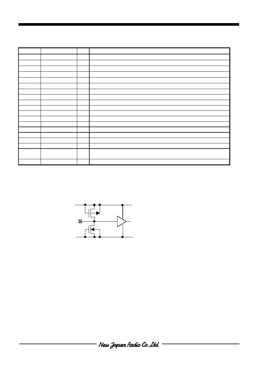
INPUT TERMINAL STRUCTURE
MCK, HALTB, D
IN1
, D
IN2
, BEEP
IN
, STBYB, SEL
V
DD
V
SS
Input Terminal

NJU3555
NJU3555
NJU8714
- 3 -
Ver.2004-05-21
FUNCTIONAL DESCRIPTION
(1) Signal Output
The OUT
1/1X
and OUT
2/2X
generate respectively L-channel and R-channel output signals, which will be
converted to analog signals via external 2nd-order or higher LC filter. A switching regulator with a high response
against a voltage fluctuation is the best selection for the V
DDO1
and V
DDO2
, which are the power supply for output
drivers. To obtain better T.H.D. performance, the stabilization of the power is required.
(2) Master Clock (MCK)
Input 1-bit audio signals such as PWM or PDM to the D
IN1
and D
IN2
pins. By setting the SEL pin to "H", master
clock (MCK) synchronizes the audio signal inputs (D
IN1
and D
IN2
). In case of "SEL" = "L", input signals go into the
amplifier circuits by own timing. Therefore, it requires careful design of PCB patterns from DSP to
NJU8714
.
The setup time and the hold time should be kept in the AC characteristics because D
IN1
and D
IN2
are fetched with
the rising edge of MCK. MCK requires jitter-free or jitter as small as possible because the jitter downs S/N ratio.
(3) Power Supply
V
DD
: Power supply for input part.
V
G
: Power supply for control logic and pre-driver which drives the transistor gates of output drivers.
It requires much higher power supply voltage than V
DDO1
and V
DDO2
for better T.H.D..
V
DDO1
, V
DDO2
: Power supply for output drivers.
(4) Output Control
Output circuit is selected by the conditions of STBYB, HALTB, SEL, D
IN1
, D
IN2
and MCK.
STBYB HALTB SEL D
IN1
, D
IN2
MCK OUT
1
OUT
2
OUT
1X
OUT
2X
L
*
*
*
H
L
*
*
*
V
SSO
V
SSO
V
SSO
V
SSO
L H *
*
*
Hi-z Hi-z Hi-z Hi-z
L V
SSO
V
SSO
V
DDO1
V
DDO2
L
H
*
V
DDO1
V
DDO2
V
SSO
V
SSO
L V
SSO
V
SSO
V
DDO1
V
DDO2
H H
H
H
V
DDO1
V
DDO2
V
SSO
V
SSO
*Don't care
BEEP circuit is operated
regardless of
STBYB and HALTB.
(5) Input Signal Synchronization Function
D
IN1
and D
IN2
are synchronized with master clock by setting SEL pin to "H".
By setting SEL pin to "L", D
IN1
and D
IN2
are
asynchronous with master clock.
(6) Output Driver Control Function
By setting HALTB pin to "L", high side output drivers become OFF and Low side output drivers become ON,
then both of OUT
1/1X
and OUT
2/2X
output V
SSO
level signals. This function works regardless of STBYB pin
setting.
(7) Standby Control Function
By setting STBYB pin to "L", the NJU8714 becomes standby condition. During standby condition, by setting
HALTB to "L", OUT
1/1X
and OUT
2/2X
become V
SSO
, and by setting HALTB pin to "H", OUT
1/1X
and OUT
2/2X
become Hi-z.
To save the power supply current at standby, MCK requires "L" level.
NJU8714
- 4 -
Ver.2004-05-21
ABSOLUTE MAXIMUM RATINGS
(Ta=25
�
C)
PARAMETER SYMBOL
RATING
UNIT
V
DD
-0.3
to
+2.75
V
G
V
DD
to +5.5
Supply Voltage
V
DDO
-0.3
to
+5.5
V
Input Voltage
Vin
-0.3 to V
DD
+0.3 V
Operating Temperature
Topr
-40 to +85
�
C
Storage Temperature
Tstg
-40 to +125
�
C
Power Dissipation
P
D
450* mW
* : Mounted on two-layer board of based on the JEDEC.
Note.1) All voltage values are specified as V
SS
=0V.
Note.2) If the LSI is used on condition beyond the absolute maximum rating, the LSI may be destroyed.
Using LSI within electrical characteristics is strongly recommended for normal operation. Use beyond
the electrical characteristics conditions will cause malfunction and poor reliability.
Note.3) The relations of V
DDO
<
V
G
must be maintained during operations.
ELECTRICAL CHARACTERISTICS
(Ta=25
�
C, V
DD
=2.5V, V
G
=5.0V, V
DDO1
= V
DDO2
=1.7V, V
SS
=V
SSO
=0V,
STBYB=HALTB=SEL=2.5V, Load Impedance=32, f
S
=44.1kHz, unless otherwise noted)
PARAMETER SYMBOL CONDITIONS
MIN
TYP
MAX
UNIT
V
DD
Supply Voltage
V
DD
-
1.7
2.5
2.7
V
DDO1
,
2
Input Voltage
V
DDO
- 0
-
2.0
V
G
Supply Voltage
V
G
-
4.5
5.0
5.25
V
Output Driver
High side Resistance
R
HPH
OUT
1
, OUT
1X
,
OUT
2
, OUT
2X
= V
DDO1
,
2
� 0.1V
V
G
=5.0V
- 1.2 2
Output Driver
Low side Resistance
R
HPL
OUT
1
, OUT
1X
,
OUT
2
, OUT
2X
= 0.1V
V
G
= 5.0V
- 1.2 2
Beep
High side Resistance
R
BEEPH
O
BEEP1
, O
BEEP2
= V
DD
� 0.1V
-
9.0
15
Power Supply Current
At Standby
I
ST
Stopping
MCK, D
IN1
, D
IN2
, BEEP
IN
STBYB= 0V
- - 1.0
uA
I
DD
-
0.05
0.1
I
DDO
-
0.25
0.5
Power Supply Current
At Operating
(Mute signal input)
I
G
No-load operating,
MCK= 256f
S
,
D
IN1
, D
IN2
= 32f
S
,
V
DDO1
= V
DDO2
= 0.18V
1.0
2.0
mA
V
IH
0.7V
DD
- V
DD
V
Input Voltage
V
IL
0
-
0.3V
DD
V
Input Leakage Current
I
LK
MCK, D
IN1
, D
IN2
, BEEP
IN
,
HALTB, STBYB, SEL
- -
�1.0
uA
Note 1) High side resistance and low side resistance depend on V
G
and V
DDO
. Therefore, V
G
and V
DDO
should be
adjusted on the application system.
Note 2) Output power using 8 speaker is 150mW(TYP:THD+N=10%) at the following condition.
V
DD
=2.5V, V
G
=5.0V, V
DDO1
= V
DDO2
=3.0V
