
NJU8725
- 1 -
CLASS D AMPLIFIER FOR DIGITAL AUDIO
!
GENERAL DESCRIPTION
The
NJU8725
is an 800mW-output class D
Amplifier featuring 6
th
modulation. It includes
Digital Attenuator, Mute, and De-emphasis circuits. It
converts digital source input to PWM signal output
which is converted to analog signal with simple
external LC low-pass filter. The
NJU8725
realizes
very high power-efficiency by class D operation.
Therefore, it is suitable for battery-powered
applications and others.
!
FEATURES
#
Stereo BTL Power Amplifier
#
Sixth-order 32f
S
Over Sampling
& PWM
#
Internal 8f
S
Over Sampling Digital Filter
#
Sampling Frequency : 96kHz (Max.)
#
De-Emphasis
: 32kHz, 44.1kHz, 48kHz
#
System Clock
: 256f
S
#
Digital Processing
: Attenuator 107step, LOG Curve
: Mute
#
Digital Audio Interface : 16bit, 18bit
:
I
2
S, LSB Justified, MSB Justified
#
Short Circuit Protection
#
Operating Voltage
: 3.0 to 3.6V
#
Driving Voltage
: V
DD
to 5.25V
#
C-MOS Technology
#
Package Outline
: SSOP24
!
BLOCK DIAGRAM
!
PIN CONFIGURATION
!
PACKAGE OUTLINE
NJU8725V
PRELIMINARY
MUTE
OUT
LP
V
DD
STBY
TEST
V
DDL
V
SSL
1
2
3
4
5
6
7
8
9
10
24
23
22
21
20
19
18
17
16
15
OUT
LN
V
DDL
MODE
LRCK
V
DDR
OUT
RN
V
SSR
OUT
RP
V
DDR
DIN
F2/SCK
F1/REQ
F0/DATA
11
12
13
14
RST
V
SS
BCK
MCK
System
Control
MUTE
STBY
F0/DATA
F2/SCK
F1/REQ
MODE
RST
32f
S
6
th
&
PWM
BCK
LRCK
DIN
Serial
Audio Data
Interface
8f
S
Over Sampling
Digital Filter
MCK
Power On
Reset Circuit
Synchronization
Circuit
V
DD
V
SS
V
DDL
V
SSL
OUT
LN
V
DDR
V
SSR
OUT
RP
V
DDR
V
SSR
OUT
RN
V
DDL
V
SSL
OUT
LP
Short Circuit
Protection

NJU8725
- 2 -
!
TERMINAL DESCRIPTION
No. SYMBOL
I/O
FUNCTION
1 V
DD
-
Logic Power Supply, V
DD
=3.3V
2 STBY
I
Standby Control Terminal
Low : Standby ON High : Standby OFF
3 TEST
I
Manufacturer Testing Terminal
Normally connect to GND.
4 MUTE
I
Mute Control Terminal
Low : Mute ON High : Mute OFF
5 V
DDL
-
Lch Power Supply, V
DDL
=V
DD
to 5.0V
6 OUT
LP
O
Lch Positive Output Terminal
7 V
SSL
-
Lch Power GND, V
SSL
=0V
8 OUT
LN
O
Lch Negative Output Terminal
9 V
DDL
-
Lch Power Supply, V
DDL
=V
DD
to 5.0V
10 MODE
I
Control Mode selection Terminal
Low : Parallel Control Mode High : Serial Control Mode
11 RST
I
Reset Terminal
Low : Reset ON High : Reset OFF
12 V
SS
-
Logic Power GND, V
SS
=0V
13 MCK
I
Master Clock Input Terminal
256f
S
clock inputs this terminal.
14 BCK
I
Serial Audio Data Bit Clock Input Terminal
This clock must synchronize with MCK input signal.
15 LRCK
I
L/R Channel Clock Input Terminal
This clock must synchronize with MCK input signal.
16 V
DDR
-
Rch Power Supply, V
DDR
=V
DD
to 5.0V
17 OUT
RN
O
Rch Negative Output Terminal
18 V
SSR
-
Rch Power GND, V
SSR
=0V
19 OUT
RP
O
Rch Positive Output Terminal
20 V
DDR
-
Rch Power Supply, V
DDR
=V
DD
to 5.0V
21
DIN
I
Serial Audio Data Input Terminal
22 F2/SCK
I
MODE="Low" : Serial Audio Interface Format Selection Terminal 2
MODE="High" : Control Register Data Shift Clock Input Terminal
The data is fetched into the control register by rise edge of SCK
signal.
23 F1/REQ
I
MODE="Low" : Serial Audio Interface Format Selection Terminal 1
MODE="High" : Control Register Data Request Input Terminal
24 F0/DATA
I
MODE="Low" : Serial Audio Interface Format Selection Terminal 0
MODE="High" : Control Register Data Input Terminal
!
INPUT TERMINAL STRUCTURE
V
DD
V
SS
Input Terminal
Inside Circuit
NJU8725
- 3 -
!
FUNCTIONAL DESCRIPTION
(1) Signal Output
PWM signals of L channel and R output from OUT
LP
/
LN
and OUT
RP
/
RN
terminals respectively. These signals
are converted to analog signal by external 2nd-order or over LC filter. The output driver power supplied from
V
DDL
, V
DDR
, V
SSL
, and V
SSR
are required high response power supply against voltage fluctuation like as switching
regulator because Output THD is effected by power supply stability.
(2) Master Clock
Master Clock is 256f
S
clock into MCK terminal for the internal circuit operation clock.
(3) Reset
"L" level input over than 3ms to the RST terminal is initialization signal to initialize the internal circuit. This
initialization signal is synchronized with internal clock and executes logical OR with the internal power on reset
signal. This Reset signal initializes the internal function setting registers also. During initialization, the
output-drivers output GND level. The reset equivalent circuit is shown bellow.
(4) 8f
S
Over Sampling Digital Filter
8f
S
Over Sampling Digital Filter interpolates
Audio data and decreases aliasing noise.
It realizes Attenuation and De-Emphasis function by serial function control.
(5) 32f
S
6
th
& PWM
32f
S
6
th
& PWM convert from Audio data of the 8f
S
Over Sampling Digital Filter to the 32f
S
one bit PWM
data.
(6) Short Circuit Protection
Short Circuit Protection protects IC with output terminal of high-impedance condition when output terminal is
shorted to GND or other output terminal.
The high-impedance condition is released automatically with master clock input, not released without master
clock input.
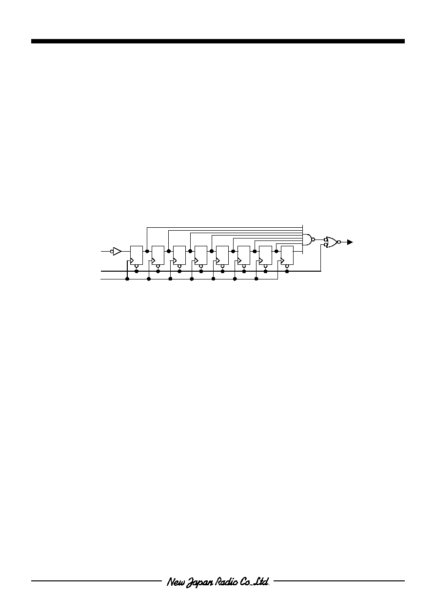
D
D
D
D
D
D
D
D
Internal Reset
RST
Power on Reset
CLK
(About 10kHz)
Figure 1. Reset Equivalent Circuit

NJU8725
- 4 -
(7) System Control
(7-1) Standby
Standby functions by "L" level input to the STBY terminal. In busy of Standby, conditions of digital audio
format set, attenuation level, de-emphasis, and attenuator operation time are kept and output terminals are
high-impedance.
(7-2) Control Mode Set
A control mode as shown below is selected by the MODE terminal.
MODE Control
Method
Function
Terminals
0
Parallel
Digital Audio interface Format Set
F0, F1, F2
1
Serial
Control Register serial data input
DATA, REQ, SCK
Parallel
: Digital Audio Interface Format is set directly by using F0, F1, and F2 terminals.
Serial :
NJU8725
is controlled serial input data by 3-wire serial interface using DATA, REQ, and
SCK terminals
By this setting, the function of F0/DATA, F1/REQ, and F2/SCK are changed.
Refer to
(8-5)F0,F1,F2 about function of F0, F1, and F2 terminals.
Refer to
(8)Control Register about function of DATA, REQ, and SCK terminals.
(7-3) Mute
Mute functions by "L" signal into the MUTE terminal. In busy of mute, a current attenuation value
becomes -
by internal digital attenuator. And MUTE is stopped by "H" signal into the MUTE terminal, the
attenuation value returns from -
to previous value.
MUTE Attenuation
Level
0
-
1 Set
Value
1024/f
S
1024/f
S
-
-
Set Value
MUTE
MCK
Attenuation Value
Set Value
Figure 2. Mute Timing

NJU8725
- 5 -
(8) Serial Audio Data Interface
(8-1) Input Data Format Selection
The digital audio interface format is selected out of I
2
S, MSB Justified or LSB Justified, and 16 bits or 18
bits data length.
(8-2) Input Timing
Digital audio signal data into DIN terminal is fetched into the internal shift register by BCK signal rising
edge. The fetched data in the shift register are transferred by rising edge or falling edge of LRCK as
shown below:
Data Format
Rising Edge
Falling Edge
I
2
S
Lch Input Register
Rch Input Register
MSB Justified
Rch
Input Register
Lch
Input Register
LSB Justified
Rch
Input Register
Lch
Input Register
BCK and LRCK must be synchronized with MCK.
Figure 3.1. 16 bits I
2
S Data Format
Left Channel
Right Channel
LRCK
BCK
DIN
14
0
1
15
13
14
0
1
15
13
Right Channel
Left Channel
Figure 3.2. 16 bits MSB Justified Data Format
LRCK
BCK
DIN
13
0
1
14
0
1
14
15
13
15
15
Figure 3.3. 16 bits LSB Justified Data Format
Left Channel
Right Channel
14
0
1
2
3
0
15
14
0
1
2
3
15
LRCK
BCK
DIN