PPRELIMINARY
Ver.1.0
NJW1104
- 1 -
DOLBY PRO LOGIC SURROUND DECODER
n
n
n
n
GENERAL DESCRIPTION
n
n
n
n
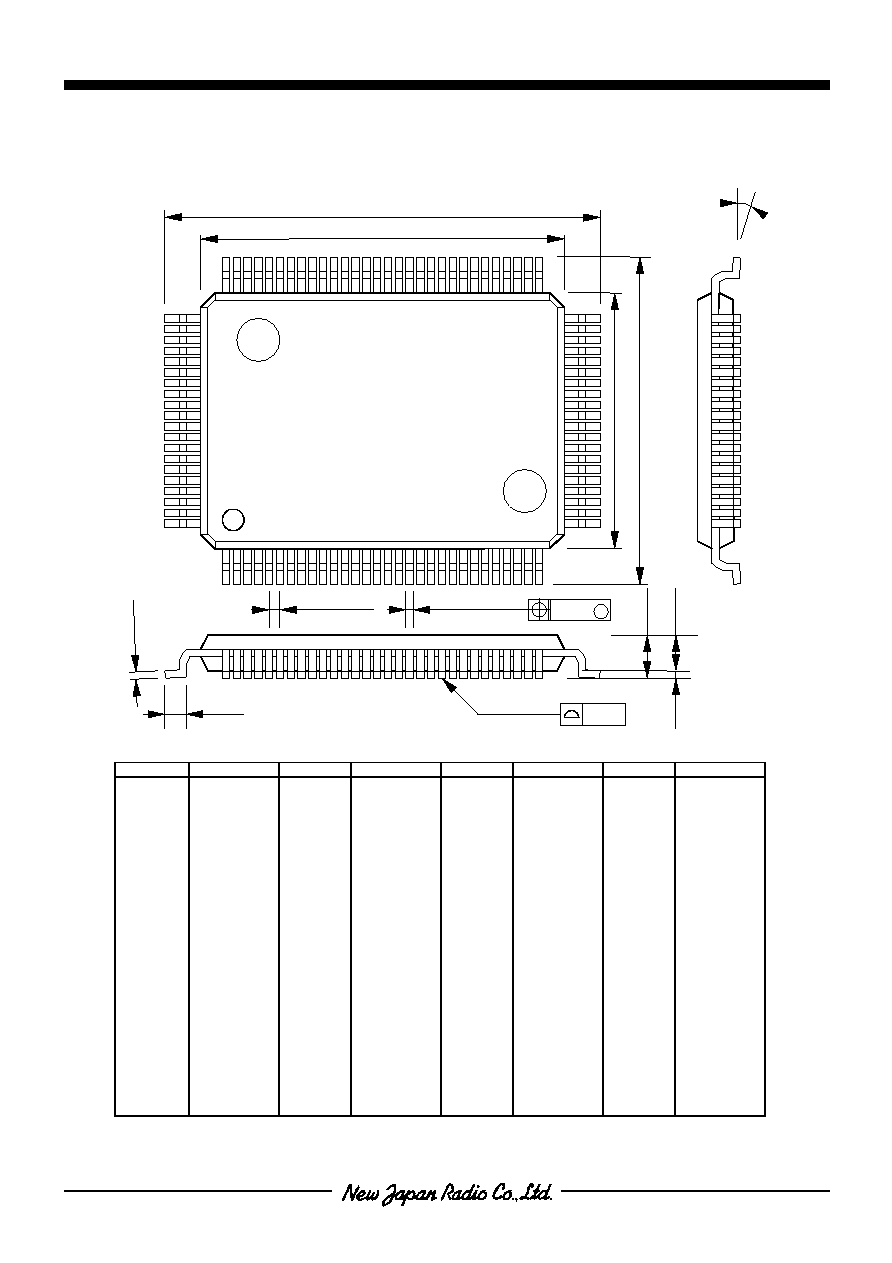
PACKAGE OUTLINE
The NJW1104 is a surround processor including all of
the necessary circuits of Dolby Pro Logic Surround
decoder and digital delay.
In addition to Dolby Pro Logic Surround function, it
performs easily other surround function such as Hall, Live,
Disco and others.
Dolby and double-D symbol are trademarks of Dolby Laboratories Licensing Corporation.
San Francisco, CA94103-4813.USA.
This device is available only to licensees of Dolby Lab.
Licensing and application information may be obtained from Dolby Lab.
n
n
n
n
FEATURES
l
Operating Voltage : V
CC
=10V(Analog Block), V
DD
=5V(Digital Block)
l
Digital Delay on chip
l
Serial Data Interface(3-wire)
DATA, REQ, SCK
l
Bi-CMOS Technology
l
Package Outline
QFP80, QFP100
n
n
n
n
FUNCTION
[Dolby Pro Logic Surround]
l
Automatic input balance
l
Noise sequencer
l
Adaptive matrix
l
Center channel control
(Wide band, Normal, Phantom, Off)
l
Modified B-type noise reduction
l
7kHz low-pass filter
l
Dolby 3 stereo mode
l
Digital time delay(15,20,25,30msec.)
[Other Surround]
l
Surround Signal Selector
(L+R, L-R, EXTIN)
l
Front mixing control
l
Digital time delay
(15,20,25,30,40,50,60msec.)
[Other Function]
l
Digital auxiliary outputs
(AUX1-AUX10)
n
n
n
n
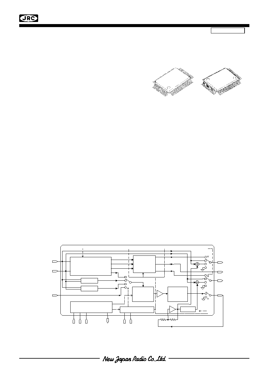
SYSTEM BLOCK DIAGRAM
EXTIN
7KHz
LPF
SW. Controller
ADD/SUB
.
L+R
L-R
Center Mode
Modified
B-NR
MCU Interface
Delay
Input Autobalance
Noise Sequencer
Adaptive Matrix
RIN
LOUT
COUT
ROUT
SOUT
LIN
DA
T
A
SC
K
RE
Q
AU
X
1
-
10
MD
1
MD
2
NJW1104FC2-80
NJW1104FC2
Ver.1.0
NJW1104
- 2 -
n
n
n
n
ABSOLUTE MAXIMUM RATING (Ta=25�C)
PARAMETER
SYMBOL
RATING
UNIT
Supply Voltage
V
CC
V
DD
13
6.5
V
Power Dissipation
*
P
D
(QFP80) 1.3
(QFP100) 1.3
W
Operating Temperature Range
T
opr
-20 to +75
�C
Storage Temperature Range
T
stg
-40 to +125
�C
*On board
n
n
n
n
ELECTRICAL CHARACTERISTICS (V
CC
=10V, V
DD
=5V, Ta=25�C)
PARAMETER
SYMBOL
TEST CONDITION
MIN.
TYP.
MAX.
UNIT
u
OVERALL
Supply Voltage Range
V
CC
V
DD
9
4.5
10
5
13
5.5
V
V
Supply Current
I
CC
I
DD
No Signal
No Signal
-
-
37
6
50
10
mA
mA
Reference Voltage
V
REF
No Signal
3.6
4.0
4.4
V
Threshold Voltage
V
thh
V
thl
Digital input high level
Digital input low level
0.7V
DD
0.0
-
-
V
DD
0.3V
DD
V
V
u
INPUT AUTO BALANCE
Capture Range
CPR
-
5
-
Error Correction
CER
-
4
-
u
ADAPTIVE MATRIX (0dB=300mVrms, f=1kHz at Cin Cout)
Output Level Accuracy
relative to Cch
D
Vol
L,R,S'ch.out
-0.5
0
0.5
dB
Matrix Rejection relative
MR
L,R,S'ch.out
25
40
-
dB
Headroom
HR-AM
V
CC
=9V at THD=1%
15
17
-
dB
Total Harmonic Distortion
THD-AM
L,R,C,S'ch.out at 4ch.mode
L,R,ch.out at 2ch.mode
-
-
0.05
0.002
0.2
0.1
%
%
Signal to Noise Ratio
SNAM
Rg=0,wt:CCIR-ARM at 4ch.mode
L,R,ch.out at 2ch.mode
75
93
80
100
-
-
dB
dB
u
NOISE SEQUENCER
Output Noise Level
Vno
-15.0
-12.5
-10.0
dB
Output Noise Level
Accuracy relative to Cch
D
Vno
L,R,S'ch.out
-0.5
0.0
0.5
dB
u
MODIFIED B-TYPE NOISE REDUCTION (0dB=300mVrms, f=100Hz at Sin Sout)
Voltage Gain
GV-NR
Vin=0dBd,f=100Hz
-
9.5
-
dB
Decode Responce1
DEC1
Vin=0dBd,f=1kHz
-1.6
-0.1
1.4
dB
Decode Responce2
DEC2
Vin=-15dBd,f=1.4kHz
-3.0
-1.5
0.0
dB
Decode Responce3
DEC3
Vin=-20dBd,f=1.4kHz
-4.9
-3.4
-1.9
dB
Decode Responce4
DEC4
Vin=-40dBd,f=5kHz
-6.8
-5.3
-3.8
dB
Total Harmonic Distortion
THDNR
Vin=0dBd,f=1kHz
-
0.07
0.3
%
Headroom
HRNR
V
CC
=9V at THD=1%
15
17
-
dB
Signal to Noise Ratio
SNNR
Rg=0,weightted:CCIR/ARM
73
78
-
dB
Ver.1.0
NJW1104
- 3 -
n
n
n
n
ELECTRICAL CHARACTERISTICS (V
CC
=10V, V
DD
=5V, Ta=25�C)
PARAMETER
SYMBOL
TEST CONDITION
MIN.
TYP.
MAX.
UNIT
u
OTHER SURROUND
Total Harmonic Distortion
THDOS
Vin=0dBd,f=1kHz
L+R,L-R output
-
0.05
0.2
dB
Headroom
HROS
V
CC
=9V at THD=1%
L+R,L-R mode
15
17
-
dB
Signal to Noise Ratio
SNOS
Rg=0,weighted:CCIR/ARM
L+R,L-R mode
75
80
-
dB
u
DIGITAL TIME DELAY
12.4
15.4
18.4
ms
17.5
20.5
23.5
ms
22.6
25.6
28.6
ms
27.7
30.7
33.7
ms
38.0
41.0
44.0
ms
48.2
51.2
54.2
ms
Delay Time
Td
f
OSC
=4MHz
58.4
61.4
64.4
ms
Total Gain
Gv
-3.0
0.0
3.0
dB
Td=15.4ms
-
0.3
0.6
%
Td=20.5ms
-
0.3
0.6
%
Td=25.6ms
-
0.4
0.8
%
Td=30.7ms
-
0.5
1.0
%
Td=41.0ms
-
0.6
1.2
%
Td=51.2ms
-
0.7
1.4
%
Total Harmonic Distortion
THD
Vin=0.3Vrms
f=1kHz
30kHz LPF
Td=61.4ms
-
0.8
1.6
%
Maximum Output Voltage
Vomax
Vin:f=1kHz
30kHz LPF,THD=3%
1.5
1.8
-
Vrms
Td=15.4ms
-
-85
-75
dBV
Td=20.5ms
-
-85
-75
dBV
Td=25.6ms
-
-85
-75
dBV
Td=30.7ms
-
-80
-70
dBV
Td=41.0ms
-
-80
-70
dBV
Td=51.2ms
-
-80
-70
dBV
Output Noise Voltage
No
Rg=600
W
Vin=0Vrms
JIS-A
Td=61.4ms
-
-75
-65
dBV
u
DIGITAL AUXILIARY OUTPUT
Low Level Output
VOL
Output Current=-1mA
0.0
-
0.3V
DD
dB
High Level Output
VOH
Output Current=1mA
0.7V
DD
-
V
DD
dB