
- 1 -
NJW1151
6-CHANNEL ELECTRONIC VOLUME
s
s
s
s
GENERAL DESCRIPTION
s
s
s
s
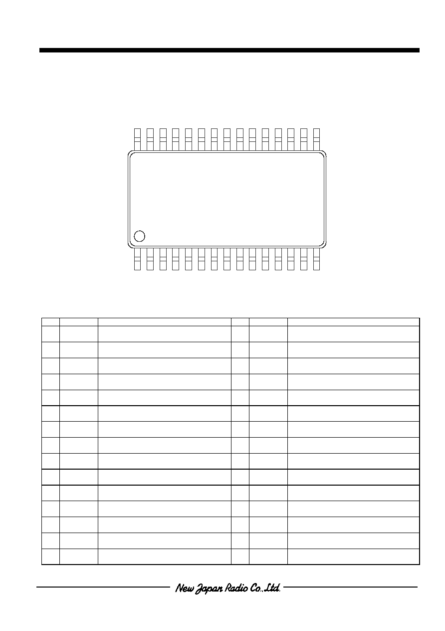
PACKAGE OUTLINE
The NJW1151 is a 6-CHANNEL ELECTRONIC VOLUME,
which also includes tone control, balance and trim level
control. The NJW1151 is suitable for multi-channel audio
system, such as AV amplifier, mini stereo component,
speaker system, and others.
All of internal status and variables are controlled by I
2
C
BUS interface.
s
s
s
s
FEATURES
q
Operating Voltage
+8.0 to +15.0V
q
I
2
C BUS Interface
q
6-Chnnel Master Volume
0 to �79dB, MUTE
q
Balance control for L, R-ch
0 to �30dB, MUTE
q
Trim Level Control for C, SL, SR, SW-ch 0 to �20dB
q
Independent Tone Control (Bass, Treble) for L, R-ch
q
Bi-CMOS Technology
q
Package Outline
SDMP30
s
s
s
s
BLOCK DIAGRAM
NJW1151M
Balance
Control
Level Trim
Master
Volume
Tone Control
Bass/Treble
I
2
C BUS
Interface
Power
Supply
+8 to +15V
Lch TONE in
Rch TONE in
Lch TONE out
Rch TONE out
Lch in
Rch in
Lch out
Rch out
C-ch in
SL-ch in
SR-ch in
SW-ch in
C-ch out
SL-ch out
SR-ch out
SW-ch out
- 2 -
NJW1151
s
s
s
s
PIN FUNCTION
No. SYMBOL
FUNCTION
No.
SYMBOL
FUNCTION
1 VREF Reference
voltage
16
SCL I
2
C bus clock input
2
V+
Power supply voltage
17
SDA I
2
C bus data input
3
VREFC
Reference voltage stabilization capacitor
18
SWOUT
Volume Sub Woofer channel output
4
RTIN
Tone control Right channel input
19
SROUT
Volume Surround Right channel output
5
RTOUT
Tone control Right channel output
20
SLOUT Volume Surround Left channel volume
output
6
RTC
Tone control Right channel
Treble filter capacitor
21
COUT
Volume Center channel output
7
RBC1
Tone control Right channel
Bass filter capacitor
22
ROUT
Volume Right channel output
8
RBC2
Tone control Right channel
Bass filter capacitor
23
LOUT
Volume Left channel output
9
RBC3
Tone control Right channel
Bass DC cut capacitor
24
LBC3
Tone control Left channel
Bass DC cut capacitor
10
LIN
Volume Left channel input
25
LBC2
Tone control Left channel
Bass filter capacitor
11
RIN
Volume Right channel input
26
LBC1
Tone control Left channel
Bass filter capacitor
12
CIN
Volume Center channel input
27
LTC
Tone control Left channel
Treble filter capacitor
13
SLIN
Volume Surround Left channel input
28
LTOUT
Tone control Left channel output
14
SRIN
Volume Surround Right channel input
29
LTIN
Tone control Left channel input
15
SWIN
Volume Sub Woofer channel input
30
GND Ground
(IC substrate)
1 15
16
30
- 3 -
NJW1151
s
s
s
s
ABSOLUTE MAXIMUM RATING (Ta=25
�
�
�
�
C)
PARAMETER SYMBOL
RATING
UNIT
Supply Voltage
V
+
+15
V
Maximum Input Voltage
V
IM
V
+
(
)
V
Power Dissipation
P
D
700
mW
Operating Temperature Range
Topr
-40 to +85
�
C
Storage Temperature Range
Tstg
-40 to +125
�
C
(
) For the maximum input voltage less than 0 to V+
s
s
s
s
ELECTRICAL CHARACTERISTICS ( Ta=25
�
�
�
�
C,V
+
=14V, V
DD
=5V)
PARAMETER SYMBOL
TEST
CONDITION
MIN.
TYP.
MAX.
UNIT
Power Supply
Operating Voltage
V
+
8.0 14.0
15.0 V
Supply Current
I
CC
No
Signal
- 10 30 mA
Input/Output Characteristics
Voltage Gain
G
V
V
IN
=1Vrms, f=1kHz
Master=0dB, Balance=0dB
Trimmer=0dB
-0.5 0 0.5 dB
Voltage Gain Error
G
V
V
IN
=1Vrms, f=1kHz
Master=0dB
-0.5 0 0.5 dB
Maximum Attenuation 1
A
TT1
f=1kHz, V
IN
=1Vrms
Master=-79dB
- -79 - dB
Maximum Attenuation 2
A
TT2
f=1kHz, V
IN
=1Vrms
Mute
- -90 - dB
Attenuation Error
A
TT
f=1kHz, V
IN
=1Vrms
Master=-50dB
Trimmer=-10dB
-1 0 1 dB
Maximum Output Voltage
V
OM
f=1kHz,THD=1%
Master=0dB
3.0 4.0 - Vrms
Output Noise
V
NO
Master=0dB,
Rg=0,A-weight
-
-110
(3.2
�
)
-100
(10
�
)
dBV
(Vrms)
Total Harmonic Distortion
T.H.D.
f=1kHz,Vo=1Vrms,
Master=0dB,Trimmer=0dB
- 0.005
0.05 %
Channel Separation
CS
f=1kHz,Vo=1Vrms
Master=0dB,A-weight
- -90 -80 dB
Tone Control Characteristics
Treble Boost Gain1
HF
BST
Vo=1Vrms f=10kHz
Treble=10dB
8 10 12 dB
Treble Boost Gain2
HF
CUT
Vo=1Vrms f=10kHz
Treble=-10dB
-12 -10 -8 dB
Bass Boost Gain1
LF
BST
Vo=1Vrms f=50Hz
Bass=10dB
8 10 12 dB
Bass Boost Gain2
LF
CUT
Vo=1Vrms f=50Hz
Bass=-10dB
-12 -10 -8 dB

- 4 -
NJW1151
s
s
s
s
I
2
C BUS Block CHARACTERISTICS (SDA, SCL)
PARAMETER SYMBOL
MIN.
TYP.
MAX.
UNIT
High Level Input Voltage
V
IH
3.0 - 5.0 V
Low Level Input Voltage
V
IL
0 -
1.5
V
High Level Input Current
I
IH
-
-
10
�A
Low Level Input Current
I
IL
-
-
10
�A
Low Level Output Voltage (3mA at SDA pin)
V
OL
0 -
0.4
V
Maximum Output Current
I
OL
-3.0 - - mA
Maximum Clock Frequency
f
SCL
- -
100
kHz
Data Change Minimum Waiting Time
t
BUF
4.7 - - �s
Data Transfer Start Minimum Waiting Time
t
HD:STA
4.0 - - �s
Low Level Clock Pulse Width
t
LOW
4.7 - - �s
High Level Clock Pulse Width
T
HIGH
4.0 - - �s
Minimum Start Preparation Waiting Time
t
SU:STA
4.7 - - �s
Minimum Data Hold Time
t
HD:DAT
0 - 3.45 �s
Minimum Data Preparation Time
t
SU:DAT
250 - - ns
Rise Time
t
R
-
-
1.0
�s
Fall Time
t
F
-
-
300
ns
Minimum Stop Preparation Waiting Time
t
SU:STO
4.7 - - �s
I
2
C BUS Load Condition: Pull up resistance 4k
(Connected to +5V)
Load capacitance 200pF (Connected to GND)
SDA
SCL
t
BU
t
HD:ST
Sr
P
t
LOW
t
R
t
HD:DA
t
HIGH
t
F
t
SU:DA
S
P
t
SU:ST
t
SU:ST
t
HD:ST

- 5 -
NJW1151
s
s
s
s
TERMINAL DESCRIPTION
No. SYMBOL
FUNCTION
EQUIVALENT
CIRCUIT
TERMINAL
VOLTAGE
1
VREF
Reference voltage
V+ / 2
2 V+
Power supply voltage
V
+
3 VREFC
Reference voltage stabilization
capacitor
V+ / 2
4
29
RTIN
LTIN
Tone control
Right channel input
Left channel input
V+ / 2
GND
GND VREF
V+
300
50K
GND
V+
V+
GND
50K
50K