 | –≠–ª–µ–∫—Ç—Ä–æ–Ω–Ω—ã–π –∫–æ–º–ø–æ–Ω–µ–Ω—Ç: NJW1508 | –°–∫–∞—á–∞—Ç—å:  PDF PDF  ZIP ZIP |
NJW1504/1508
- 1 -
PLL Synthesizer with I
2
C Bus for TV Tuner
n
DESCRIPTION
The NJW1504/1508 are a PLL frequency synthesizer especially
designed for TV and VCR tuning systems and consists of PLL circuit
and a prescaler which operates up to 1.0GHz, built into one chip.
The NJW1504/1508 are controlled through an I
2
C-bus.
n
FEATURES
∑
Operating Voltage 5V
∑
Low Operating Current : 15mA typ. @Vcc=5V
∑
Prescaler accepts frequencies up to 1GHz on chip
∑
Reference Signal :
NJW1504: Reference Signal Oscillator with peripheral of Xtal on chip
NJW1508: Buffer Amplifier for External Reference Signal on chip
∑
34V max. tuning voltage output
∑
Package Outline: SSOP16
n
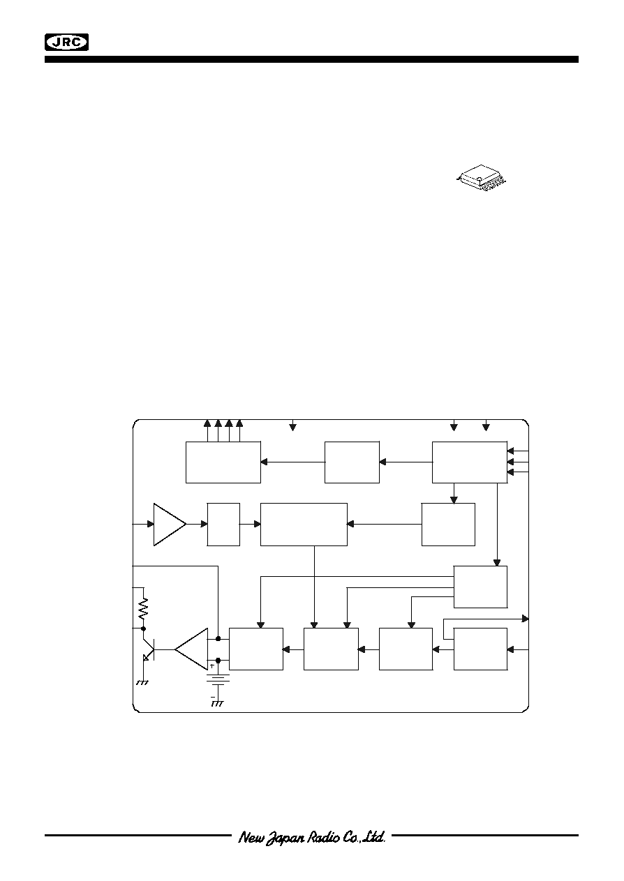
BLOCK DIAGRAM
(Note)
Purchase of I
2
C components of New Japan RadioCo.,Ltd or one of its sublicensed Associated Companies conveys a license
under the Philips I
2
C Patent Rights to use these components in an I
2
C system, provided that the system conforms to the I
2
C
standard specification as definedby by Philips.
n
PACKAGE OUTLINE
NJW1504V/NJW1508V
BS0-BS3
BAND SW
4bit
4bit
Latch
VCC3
VCC1
5V
GND
ADRS
SDA
SCL
I2C
Bus
Receive
r
15bit
Latch
8bit
Latch
Programmable
Divider 15bit
PreAMP
1/8
CP
VCC2
AMPOUT
HF IN
AMP
Phase
OUT
Phase
Comp.
1/1024
1/512
(1/640)
Ref.
Divider
X'tal
OSC
OSCOUT
XTAL
NJW1504/1508
- 2 -
n
ABSOLUTE MAXIMUM RATINGS (T
A
=25
∞
C)
Parameter
Symbol
Ratings
Unit
Supply Voltage (Vcc1, 3)
Vcc1, Vcc3
-0.3 to +6.5
V
Supply Voltage (Vcc2)
Vcc2
-0.3 to +36
V
Input Voltage (except I
2
C bus)
Vi
-0.3 to Vcc+0.3
V
Output Voltage (except I
2
C bus)
Vo
-0.3 to Vcc+0.3
V
I
2
C bus Input Voltage
V
iiic
-0.3 to 6.5
V
Power Dissipation
P
D
300
mW
Operating Temperature Range
T
opr
-20 to +85
∞
C
Storage Temperature Range
T
stg
-40 to +125
∞
C
n
RECOMMENDED OPERATING CONDITION (T
A
=25
∞
C)
Parameter
Condition
Symbol
Min.
Typ.
Max.
Unit
Operating Voltage
Vcc1, Vcc3
Vcc1, Vcc3
4.5
5
5.5
V
Operating Voltage
Vcc2
Vcc2
0
-
34
V
X'tal Operating Range
f
xtal
3.15
4
4.05
MHz
HF Input Frequency
Input= -20dBm
f
hf
80
-
1000
MHz
Clock Frequency
f
SCL
0
-
100
KHz
Bus Free Time
t
BUF
4.7
-
-
uS
Data Hold Time
t
HDSTA
2
-
-
uS
SCL Low Hold Time
t
LOW
4.7
-
-
uS
SCL High Hold Time
t
HIGH
2
-
-
uS
Set-up Time
t
SUSTA
2
-
-
uS
Data Hold Time
t
HDDAT
0
-
-
uS
Data Set-up Time
t
SUDAT
250
-
-
nS
Rise Time
t
R
-
-
1000
nS
Fall Time
t
F
-
-
300
nS
Data Set-up Time
Refer to I
2
C bus Timing Chart
t
SUSTO
4
-
-
uS
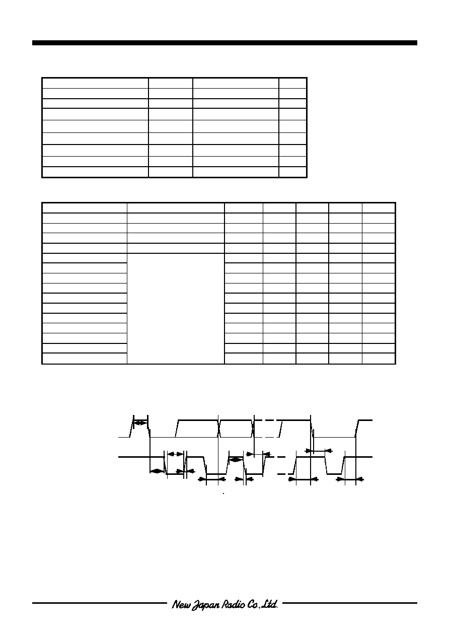
I
2
C bus Timing Chart
V
IH
min(0.7 Vcc1) and V
IL
max(0.3 Vcc1)
S C L
S D A
t
B U F
t
L O W
t
H D ; S T A
t
R
t
H D ; D A T
t
H I G H
t
F
t
S U ; D A T
t
S U ; S T A
t
H D ; S T A
t
S U ; S T O
NJW1504/1508
- 3 -
n
ELECTRICAL CHARACTERISTICS (Vcc1,3=5V,Vcc2=34V,T
A
=25
∞
C)
Parameter
Condition
Symbol Min.
Typ.
Max.
Unit
Operating Current 1
f
HF
=100MHz
I
CC
12
15
21
mA
Operating Current 2
AMPOUT: Low Level
I
CC
2
-
1.6
-
mA
AMP Input Current
Phase OUT: High Imp (2.5V)
I
IN
(-50)
0.1
(50)
nA
AMP Output Current
ANP OUT: Low Level
AMPOUT Input=5V
I
OUT
-
-
-2
mA
AMP Gain
f=1KHz
AV
40
50
60
dB
Phase Comparator
Output Current
Current Source
I
sourse
190
280
400
uA
Phase Comparator
Output Current
Current Sink
I
sink
-400
-280
-190
uA
Band Switch
"L" Output Current
BS0=BS1=0.3V
I
OBS0-1L
-2.0
-1
0
mA
"H" Output Current
BS0=BS1=4.7V
I
OBS0-1H
11.0
15.0
-
mA
"L" Output Current
BS2=BS3=0.3V
I
OBS2-3L
-2.0
-1.0
0
mA
"H" Output Current
BS2=BS3=4.7V
I
OBS2-3H
5.5
7.5
-
mA
I
2
C bus
"H" Input Current
SCL, SDA Terminal
I
IN
H
-5
0
5
uA
"L" Input Current
SCL, SDA Terminal
I
IN
L
-5
0
5
uA
"H" Input Voltage Range
SCL, SDA Terminal
V
IH
3.5
-
5.3
V
"L" Input Voltage Range
SCL, SDA Terminal
V
IL
0
-
1.5
V
ACK Sink Current
ACK Output, SDA=0.4V
V
ACK
3
-
-
mA
NJW1504/1508
- 4 -
n
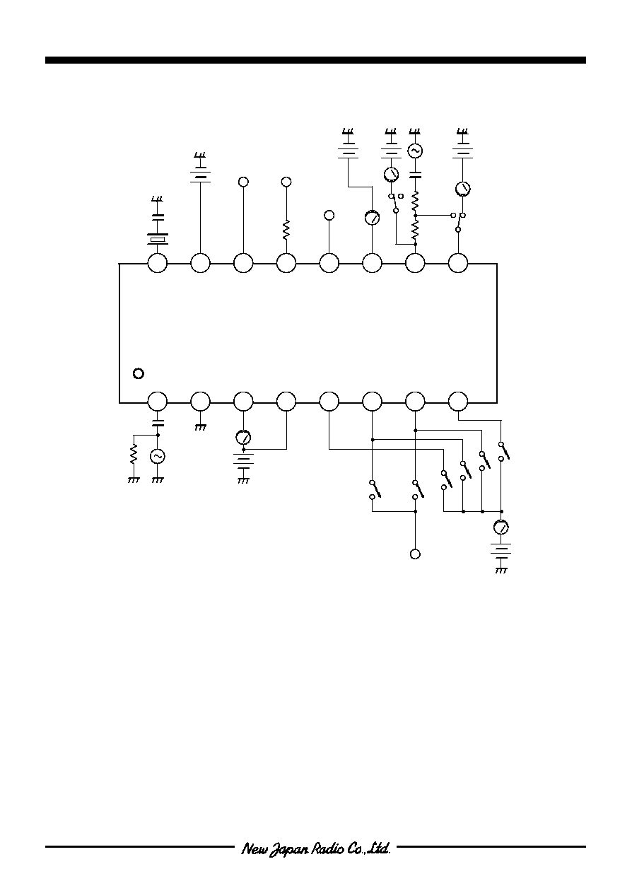
TEST CIRCUIT
1 6
HF
GND
VCC1
VCC3
BS3
BS2
BS1
BS0
XTAL
ADRS
SDA
SCL
OSC OUT
VCC2
AMP OUT
CP
1 5
1 4
1 3
1 2
1 1
1 0
9
8
7
6
5
4
3
2
1
4 M H z
5 V
1 0 0
3 4 V
V S 3
5 V
2 m V
1 k H z
V S 2
2 . 5 V
V S 1
4 . 7 V o r 0 . 3 V
C O U N T E R
5 V
5 0
S G
- 2 0 d B m
1 n
1 8 p
O S C O U T
S C L
S D A
2 7 0
3 1 6 k

NJW1504/1508
- 5 -
n
I
2
C bus Protocols
The input information, which consists of chip address and next two or four byte data, is received by I
2
C bus
receiver. The allowable I
2
C bus protocols are as follows.
(1) STA CA CB BB STO
(2) STA CA D1 D2 STO
(3) STA CA CB BB D1 D2 STO
(4) STA CA D1 D2 CB BB STO
STA: Start Condition
STO: Stop Condition
CA: Chip Address
CB: Control Byte
BB: Band switch Byte
D1: Divider Byte 1
D2: Divider Byte 2
For suitable circuit operation,5-byte data should have chip address, 2-byte control data, band data, and 2-byte
divider byte. Following chip address. 2-byte data is received. For distinction of each data, first and third data
byte has a function bit. As function bit, divider byte has "1" and control/band data has "0".
1-7
9
S D A
S C L
S T A
A D D R E S S
R/W
1 -7
A C K
D A T A
8
8
9
9
A C K
A C K
S T O