Preliminary
NJW4302
- 1 -
THREE-PHASE DC BRUSHLESS MOTOR CONTROL IC
s
GENERAL DESCRIPTION
The NJW4302 is a three-phase DC brushless motor
pre-driver IC for precision applications.
The NJW4302 consists of PWM driver, motor velocity
control, FG(Frequency Generator) output, and voltage
velocity integration circuit.
The NJW4302 realizes stabilized velocity and it is suitable
for printer, FAX, and other DC motor control systems.
s
FEATURES
∑
Speed discriminator and PLL speed
control circuit
∑
Direct PWM driver
∑
CR oscillator
∑
Lock protection output
∑
Break circuit (short circuit braking)
∑
Start/stop switch Start/Stop Switch Circuit
∑
Current limit circuit
∑
Thermal shut down/Under voltage
lockout circuit
∑
FG output amplifier/Integrating circuit
∑
Shunt regulator output : 5V
∑
Bi-CMOS technology
∑
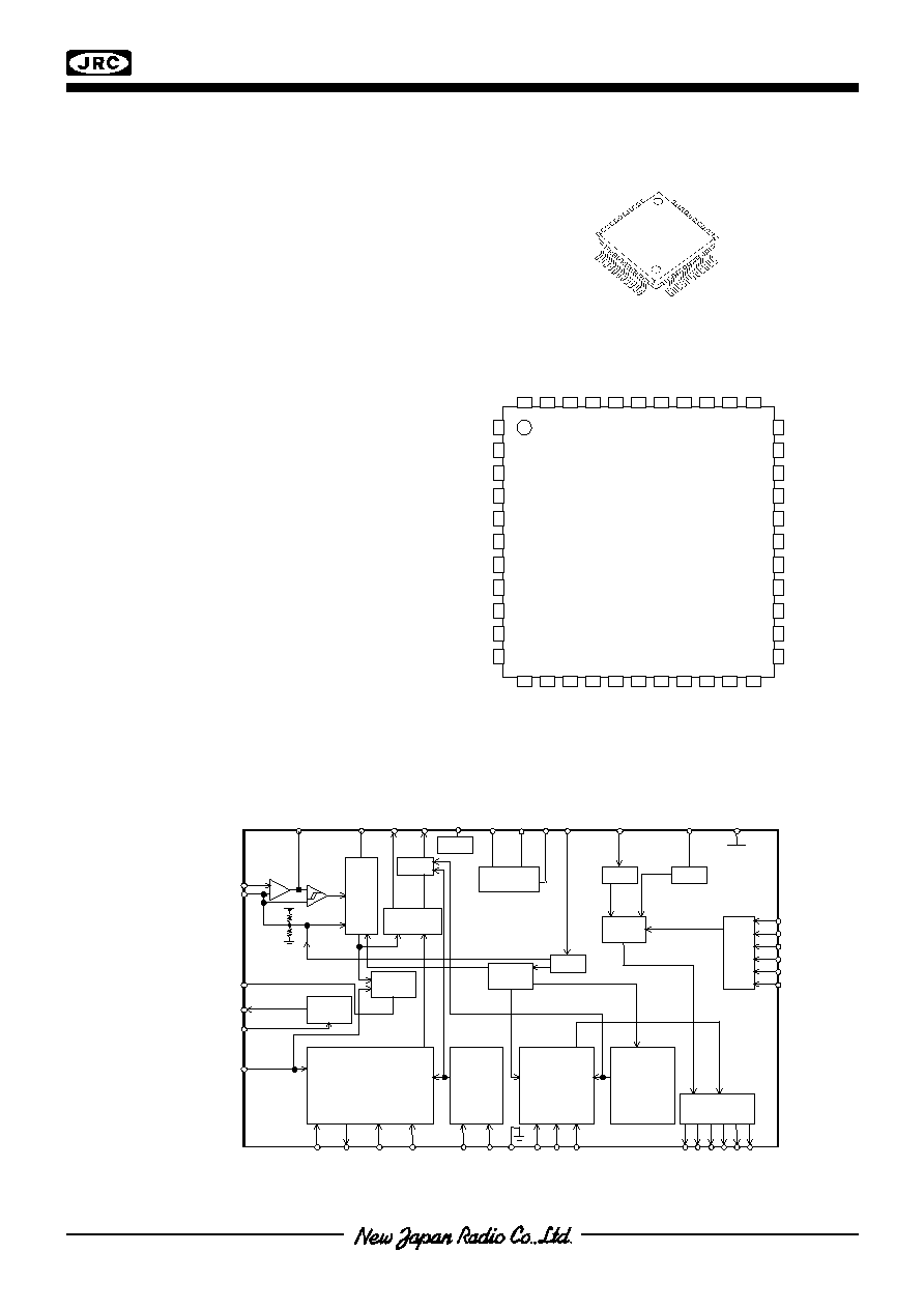
PACKAGE OUTLINE QFP44
s
PIN CONFIGRATION
PVCC
VCC
VREG
DGND
AGND
VSH
CR
CROCK
R
C
WH
FILO
FILI
INTREF
TOC
INTOUT
INT IN
DOUT
POUT
LD
BR
FR
WL
VH
VL UH
UL RF
H3
H3
H2
H2
H1
H1+
FGIN+
FGIN-
FGOUT
FGSOUT
PGND
AGND
N2
N1
SS
CLK
NJW4302 QFP44
NJW4302 QFP44
NJW4302 QFP44
NJW4302 QFP44
s
BLOCK DIAGRAM
s
PACKEGE
OUTLINE
NJW4302FA1
PLL C OU N TER
ALTER N ATIVE
C OU N TER
C IR CU IT
PWM BLOC K
PR OTEC TION
C IR C U IT
TSD / L VD S
PR I- D R IVER
-
+
-
+
FG
V
R EG
1
SPEED
PL L
SPEED
D I SC RIMI N ATOR
V
R EF
L D
S/S
IN TEGR ATION
AMP
BR
F/R
L OGIC
H AL L
H YS
AMP
C L K
Vreg
Pou t
FGIN
+
FGIN-
FGO
FGSO
O
D o ut
L D
IN TR EF
F
IN TIN IN TOU TS/S
BR
F/R
H1
+
H1 -
H2
+
H2 -
H3
+
H3 -
U L VL WL U H VH WH
TOC
R F
C R
GN D
N 2
N 1
V
+
VC O
O U T
C R OC K
ROC K
OSC
VSH
FILI
FILO
R
C
Preliminary
NJW4302
- 2 -
s
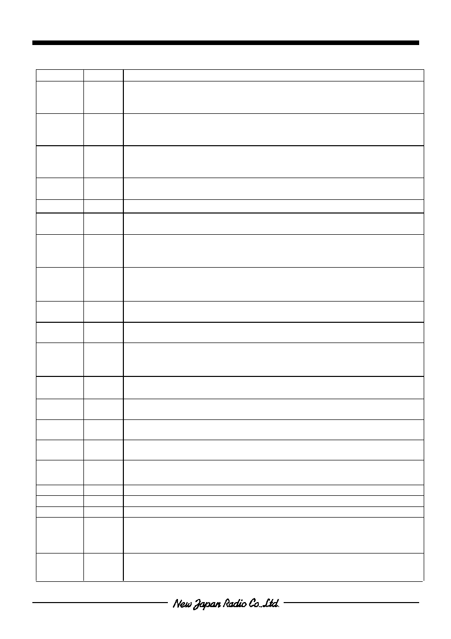
PIN DESCRIPTION
SYMBOL PIN
No.
DESCRIPTION
H1+,H1-
H2+,H2-
H3+,H3-
33, 34
35, 36
37, 38
Hall input pins
Positive input terminal is defined as IN
+
,Negative input terminal as IN
-
respectably.
Positive input is defined as IN
+
> IN
-
as Negative.
UH
VH
WH
41
43
1
Output pins(for fixed current source )
UL
VL
WL
40
42
44
Output pins(open collector sink outputs).
Duty control implement with PWM signal.
VPCC
VCC
2
3
Power-supply voltage pin
Connect a noise decoupling capacitor between these pins and the ground.
VREG
4
Shunt regulator output pin
PGND.DGND
AGND
5,6
27,28
Ground pins
These pins are all connected internally to the ground(GND).
VSH
7
Shunt regulator ON/OFF output pin
"H" or open:ON
"L":OFF
CR
8
PWM oscillator frequency setting pin
Three blocks use the oscillator: motor constraint detection circuit, clock disconnection protection circuit
and others
CROCK
9
Reference clock signal oscillator pin
Connect a capacitor between this pin to the ground.This oscillator provides clock signal when motor is locked.
R
10
VCO oscillation frequency setting pin
Connect a resistor between this pin and the ground.
C
11
VCO oscillation frequency setting pin
Connect a resister between this pin and ground.
Set the value of the capacitor so that the oscillator frequency does not exceed 1MHz.
FILI
13
VCO filter amplifier input pin
This pin is connected to VCO PLL output with 10K resistor internally in the IC.
FILO
12
VCO filter amplifier output pin
This pin is connected to VCO circuit internally in the IC.
D OUT
18
Speed discriminator output pin
Output"L"level for over speed.
P OUT
19
PLL output pin
Output the phase comparison result for 1/2fCLK and1/2fFG.
LD
20
Lock detection output pin
Open collector becomes"L"within the speed lock range(±6.25).
INT REF
14
Integrating amplifier forward rotation input(a potential of 1/2V
+
)
INT IN
17 Negative input for Integration amplifier
INT OUT
16 Output for Integration amplifier
TOC
15
Torque command input pin
This pin is normally connected to the INT OUT pin. When the TOC voltage level falls,the UL,VL and Wl PWM duties are
changed to increase.
FG IN+
32
Input pin for FG amplifier forward rotation (a potential of 1/2V
+
)
Connect a noise decoupling capacitor between V
+
terminal and the ground.

Preliminary
NJW4302
- 3 -
FG IN-
31 FG
amplifier reverse rotation input.
FGOUT 30 FG
amplifier output.
FGSOUT
29
FG amplifier output(after the schmitt)
Open collector output.
RF
39
Output current detection
Connect a resistor between this pin and GND pin.The output limitation maximum current(IOUT)is set to be 0.5/Rf.
SS 24
Start
Stop control
"L":Start
"H"or Open:Stop
FR
22
Forward/reverse rotation control
"L":Forward
"H"or Open:reverse
BR
21
Brake control (short braking operation)
"L":Start
"H"or Open:Brake
CLK
23
External clock signal input
10kHz max.
N1
N2
25
26
Speed discriminator count switching

Preliminary
NJW4302
- 4 -
s
FUNCTIONAL DESCRIPTION
1. VCO circuit
The variable range of PLL circuit is determined by two factors: VCO frequency determined by RC value connected
to Pin 15 and Pin 16 and VCO loop filter constants. VCO frequency range must be within 160kH
Z
to 1.0MH
Z.
The typical external value is as follows:
R=20k,C=100pF.
The filter constants are C=0.47µF,R=27k.
2. Output drive circuit
The PWM control is made by upper side of external transistor.
3. Speed lock range
The speed lock range is ±6.25% of fixed speed. When the motor speed is within the lock range, the LD pin
(an open collector output)goes "L". If the motor speed goes out of the lock range, the LD pin goes "H".
Please be noted that the LD signal may go on during startup.
4. PWM frequency
The PWM frequency is determined by resistor and capacitor value connected to the CR pin.
The PWM frequency is given by expressed as:
f
PWM
=
1/(0.48CR)
When C=1500pF,R=75K,the PWM frequency goes about 19KHz.
5. Lock detection circuit(CLOCK)
Lock detection circuit protects the driver IC and the motor from fatal over current failure when the motor is
locked during startup. If the LD output remains "H" (motor lock state) for a certain period (Hold time),all phase of upper
side transistors are to be turned off.
The hold time can be programmed by capacitor value attached to the CLOCK pin by the following:
Set time(sec) =66◊C(µF)
With C=0.068µF,the hold time can be programmed for approximately 4.5 sec.
Once Lock detection circuit is activated, the state remains unchanged unless it is turned off, or stopped.
This function can be disabled when the CLOCK pin is connected to the ground.
6. Forward / Reverse(F/R)Switching
The direction control can be made with the state of the F/R pin. The direction can be changed even during the
motor in motion.

Preliminary
NJW4302
- 5 -
7. Brake Switch
NJW4302 uses a short brake method that turns on all phase of upper side transistors for braking. During the
time, all lower side transistors are turned off.
8. VREG pin/VSH pin
NJW4302 includes a regulator to generate for +5V regulated IC supply when the motor drive circuit
is designed with a single power supply. The VREG pin and V+ pin compose a shunt regulator for 5V±5%
output with a external resistor and a transistor. To use the regulator, the VSH pin must be either "H", or Open.
Otherwise, the VSH pin must be "L" and the VREG pin is to be opened.
9. Frequency Generator (FG) Amplifier
The internal FG amplifier with few passive components composes a filter amplifier shown in the
application. Circuit for noise rejection. The output voltage of the amplifier must be at least 250mA p-p since it feature
Schmitt comparator.
The capacitor connected between the FGIN+ pin and the ground is necessary for bias voltage
stabilization and initial reset pulse generation for the internal logic. The reset pulse is generated when the
FGIN+ pin goes from 0 to approximately 1.25V.
10. Integration Amplifier
The integration amplifier integrates the D-out and P-out and converts them to speed command voltage. During the
time, it also sets the control loop gain and frequency characteristics using external components.
11. Speed Control Circuit
NJW4302 features two speed control method; speed discriminator
circuit with PLL circuit and phase
comparison circuit. The FG pulse frequency is controlled to be the same frequency with a clock frequency input to the CLK
pin. Therefore, the motor speed can be controlled by changing the clock frequency.
The motor speed (N) can be expressed as:
N=CLK (Hz)◊(60/FGP)[RPM] ( FGP: Number of FG pulse per one rotation)
Given that the oscillation frequency range is 160kHz~1.0MH
Z
and the number of counts is 1024,the range of
clock frequency is 156H
Z
~960H
Z ,
and therefore the motor speed can be changed from 260rpm to 1600rpm.

Preliminary
NJW4302
- 6 -
s
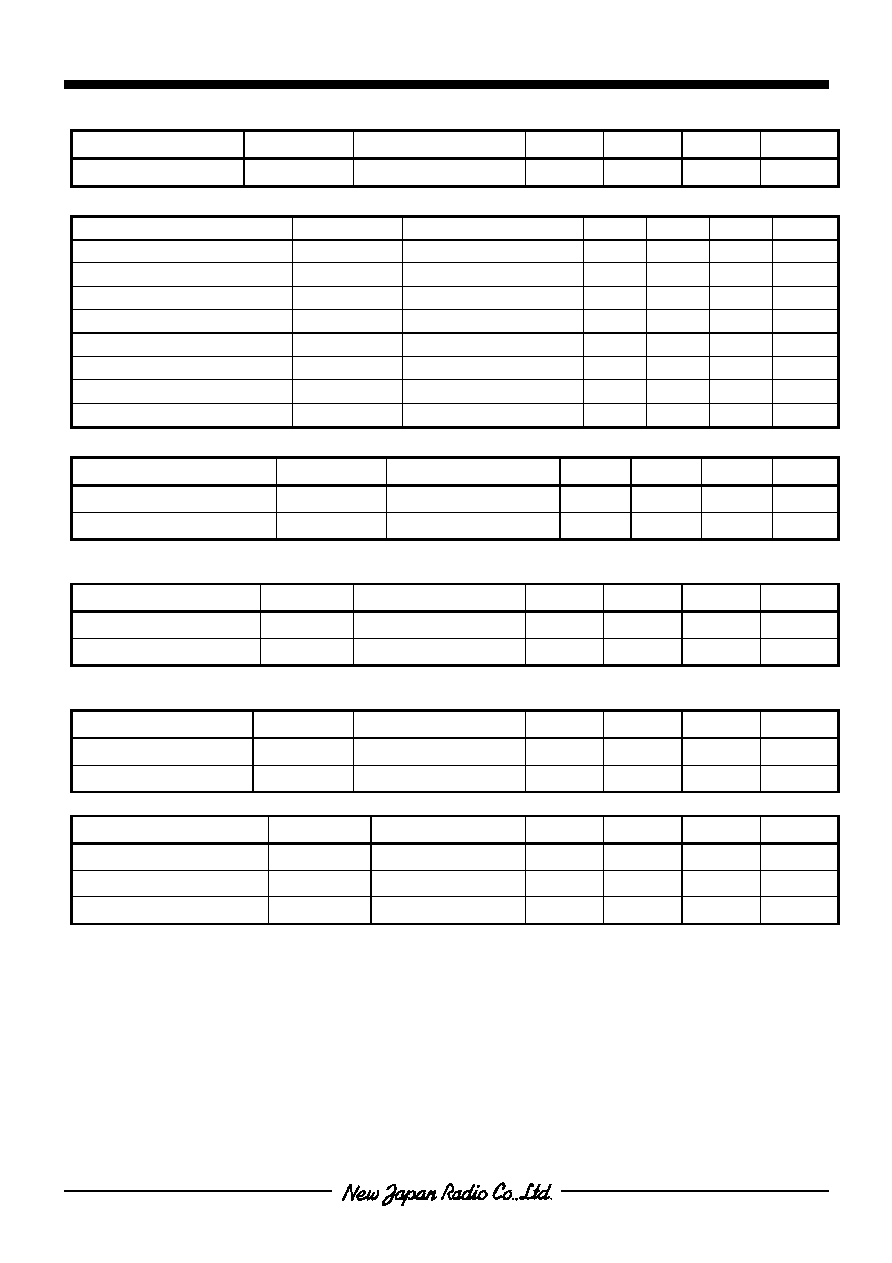
ABSOLUTE MAXIMUM RATING
PARAMETER SYMBOL
TEST
CONDITION
RATINGS
UNIT
Maximum supply voltage
V+
7
V
Maximum input current
Ireg
Vreg pin(5.6V)
10
mA
Output current
Io
UL,VL,WL
30
mA
Operating temperature
Topr
-40
85
∞
C
Storage temperature
Tstg
-55
150
∞
C
Power dissipation
Pd
700
mW
s
ALLOWABLE MAXIMUM RANGES/Ta=25
∞
∞
∞
∞
C
PARAMETER SYMBOL
CONDITION
RATINGS
UNIT
Input current range
I
REG
V
REG pin=
5.6V 1.0~5.0
mA
FG Schmitt output applied voltage
V
FGSO
0~8
V
FG Schmitt output current
I
FGSO
0~5
mA
Lock detection output current
I
LD
0~20 mA
Supply voltage
V
+
4.5~5.5 V

Preliminary
NJW4302
- 7 -
s
ELECTRICAL CHARACTERISTICS / Ta=25
∞
∞
∞
∞
C,V+=5.0V
PARAMETER SYMBOL
CONDITION
MIN.
TYP.
MAX.
UNIT
Supply current 1
I
CC
1
-
38
55
mA
Supply current 2
I
CC2
in
stop
mode
-
8
18 mA
Output saturation voltage
V
O
(sat) UL,VL and WL terminal Io=20mA
-
0.2
0.7
V
Output current
I
O
UH,VH and WH
t
erminal
Vout=1.4V
-20 -16 -12 mA
Output leakage current
I
O
(leak) UL,VL,WL
output
-
-
100
µA
Output off voltage
V
O
(off) UH,VH,WH
output
-
-
0.5
V
∑
HALL AMPLIFIER
PARAMETER SYMBOL TEST
CONDITION
MIN.
TYP.
MAX.
UNIT
Input bias current
I
HB
(HA) -4
-1
-
µ
A
Common mode input voltage range
V
ICM
1.5
-
VCC-1.5
V
Hall input sensitivity
V
IN
(HA)
-
60
-
mV
P-P
Hysteresis
V
IN
(HA)
17
32
60
mV
Input voltage Low High
V
SLH
8 16 30 mV
Input voltage High Low V
SHL
-30
-16
-8
mV
∑
∑
∑
∑
CR OSCILLATOR
PARAMETER
SYMBOL TEST
CONDITION MIN. TYP. MAX. UNIT
Output high level voltage
V
OH
(CR)
2.4
2.7
3.0
V
Output low level voltage
V
OL
(CR)
1.3
1.6
1.9
V
RC oscillation frequency
f(CR)
R=75k,C=1500pF -
19
-
kHz
RC oscillation voltage
V(CR)
0.9
1.1
1.3
V
P-P
∑
∑
∑
∑
CLOCK OSCILLATOR
PARAMETER SYMBOL
TEST
CONDITION
MIN.
TYP.
MAX.
UNIT
Output high level voltage
V
OH
(RK)
2.7
3.0
3.3
V
Output low level voltage
V
OL
(RK)
0.1
0.4
0.7
V
External capacitor charge current
I
CHG
1
- -10 -
µ
A
External capacitor discharge current
I
CHG
2
- 10 -
µ
A
Clock oscillation frequency
f
(RK)
C=0.068µF
- 35 - Hz
RC oscillation voltage
V
(RK)
2.4
2.6
2.8 V
P-P
∑
VCO OSCILLATOR (PLL COUNTER)
PARAMETER SYMBOL
TEST
CONDITION
MIN.
TYP.
MAX.
UNIT
C - terminal high-level output voltage
V
OH
(C)
1.15 1.25 1.35 V
C - terminal low-level output voltage
V
OL
(C)
0.9 1.0 1.1 V
VCO oscillation frequency
f
(C)
-
-
1.0
MHz
Amplitude V
(C)
0.15
0.25
0.6
V
P-P
Preliminary
NJW4302
- 8 -
∑
∑
∑
∑
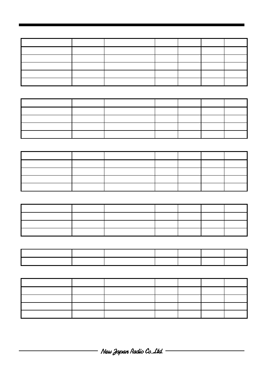
CURRENT LIMITING OPERATION
PARAMETER SYMBOL
TEST
CONDITION
MIN.
TYP.
MAX.
UNIT
Limiter V
RF
0.47
0.52
0.57
V
∑
∑
∑
∑
FG AMPLIFIER
PARAMETER SYMBOL
TEST
CONDITION
MIN.
TYP.
MAX.
UNIT
Input offset voltage
V
IO
(FG)
-10 0 10 mV
Input bias current
I
B
(FG)
-1 0 1
µ
A
Output low-level voltage
V
OH
(FG)
V
+
-1.5 V
+
-1.0 - V
Output high-level voltage
V
OL
(FG)
-
1 1.5 V
FG input sensitivity
V
IN
(
FG
)
GAIN
=40dB
- 3 - mV
Schmitt amplifier for next stage
V
SH
(FG)
100 180 250 mV
Operating frequency range
FG
- 16 - kHz
Open loop gain
AV(
FG
) f
(FG)
=2kHz -
51
-
dB
∑
∑
∑
∑
FGSO OUTPUT
PARAMETER SYMBOL
TEST
CONDITION
MIN.
TYP.
MAX.
UNIT
Output saturation voltage
V
O(FGSO)
I
O(FGS)
=2mA -
0.1
0.5
V
Output leak current
I
L(FGSO)
V
O
=V
+
-
-
10
µ
A
∑
SPEED DISCRIMINATOR OUTPUT (Dout)
PARAMETER SYMBOL
TEST
CONDITION
MIN.
TYP.
MAX.
UNIT
Output high-level voltage
V
OH(D)
V
+
-1.0 V
+
-0.7 - V
Output low-level voltage
V
OL(D)
- 0.4 - V
∑
SPEED CONTROL PLL OUTPUT (Pout)
PARAMETER SYMBOL
TEST
CONDITION
MIN.
TYP.
MAX.
UNIT
Output high-level voltage
V
OH(P)
3.35
3.65 3.95
V
Output low-level voltage
V
OL(P)
1.35 1.65 1.95
V
∑
∑
∑
∑
LOCK DETECTION (LD)
PARAMETER SYMBOL
TEST
CONDITION
MIN.
TYP.
MAX.
UNIT
Output saturation voltage
V
OL
(LD)
I
LD
=10mA -
0.1
0.5
V
Output leak current
I
L
(LD)
V
O
=V
+
- - 10
µ
A
Lock range
LOCK
Design target spec
-6.25
-
+6.25
%

Preliminary
NJW4302
- 9 -
∑
∑
∑
∑
INTEGRATER AMPLIFIER
PARAMETER SYMBOL
TEST
CONDITION
MIN.
TYP.
MAX.
UNIT
Input offset voltage
V
IO
(INT)
-10
-
10
mV
Input bias current
I
B
(INT)
-0.4
-
0.4
µ
A
Output high-level voltage
V
OH
(INT)
V
+
-0.12 V
+
-0.8 - V
Output low-level voltage
V
OL
(INT)
-
0.8
1.2
V
Open loop gain
AV(
INT
)
-
60
-
dB
Gain-band width product
GBW(
INT
)
- 1.6 - MHz
Reference voltage
V
B
(INT)
2.375 2.5 2.625
V
∑
∑
∑
∑
FILTER AMPLIFIER (PLL COUNTER)
PARAMETER SYMBOL
TEST
CONDITION
MIN.
TYP.
MAX.
UNIT
Input bias current
I
B(FIL)
- 0.4 -
µ
A
Output high-level voltage
V
OH(FIL)
V
+
-1.2 V
+
-0.8 - V
Output low-level voltage
V
OL(FIL)
-
0.8
1.2
V
Hysteresis V
B(FIL)
2.375 2.5 2.625 V
∑
∑
∑
∑
S/S AMPLIFIER
PARAMETER SYMBOL
TEST
CONDITION
MIN.
TYP.
MAX.
UNIT
Input high-level voltage
V
IH(S/S)
3.5
4.2
V
+
V
Input low-level voltage
V
IL(S/S)
0
0.8
1.0
V
Hysteresis
V
IN(S/S)
1.0 1.3 1.6 V
Pull-Up resistance
R
U(S/S)
60
80
100
k
∑
∑
∑
∑
F/R AMPLIFIER
PARAMETER SYMBOL
TEST
CONDITION
MIN.
TYP.
MAX.
UNIT
Input high-level voltage
V
IH(F/R)
3.5
4.2
V
+
V
Input low-level voltage
V
IL(F/R)
0
0.8
1.0
V
Hysteresis
V
IN(F/R)
1.0 1.3 1.6 V
Pull-Up resistance
R
U(F/R)
60
80
100
k
∑
∑
∑
∑
BR AMPLIFIER
PARAMETER SYMBOL
TEST
CONDITION
MIN.
TPY.
MAX.
UNIT
Input high-level voltage
V
IH(BR)
3.5
4.2
V
+
V
Input low-level voltage
V
IL(BR)
0
0.8
1.0
V
Hysteresis
V
IN(BR)
1.0 1.3 1.6 V
Pull-Up resistance
R
U(BR)
60
80
100
k
Preliminary
NJW4302
- 10 -
∑
∑
∑
∑
CLK AMPLIFIER
PARAMETER SYMBOL
TEST
CONDITION
MIN.
TPY.
MAX.
UNIT
Input high-level voltage
V
IH(CLK)
3.5
4.2
V
+
V
Input low-level voltage
V
IL(CLK)
0
0.8
1.0
V
Hysteresis
VI
N(CLK)
1.0 1.3 1.6 V
Pull-Up resistance
R
U(CLK)
60
80
100
k
Input frequency
f
(CLK)
- 16 - kHz
∑
N1 AMPLIFIER
PARAMETER SYMBOL
TEST
CONDITION
MIN.
TYP.
MAX.
UNIT
Input high-level voltage
V
IH(N1)
3.5
4.2
V
+
V
Input low-level voltage
V
IL(N1)
0
0.8
1.0
V
Hysteresis
V
IN(N1)
1.0 1.3 1.6 V
Pull-Up resistance
R
U(N1)
60
80
100
k
∑
∑
∑
∑
N2 AMPLIFIER
PARAMETER SYMBOL
TEST
CONDITION
MIN.
TYP.
MAX.
UNIT
Input high-level voltage
V
IH(N2)
3.5
4.2
V
+
V
Input low-level voltage
V
IL(N2)
0
0.8
1.0
V
Hysteresis
V
IN(N2)
1.0 1.3 1.6 V
Pull-Up resistance
R
U(N2)
60
80
100
k
∑
∑
∑
∑
UNDER VOLTAGE LOCKOUT
PARAMETER SYMBOL
TEST
CONDITION
MIN.
TYP.
MAX.
UNIT
Operating voltage
V
SDL
-
3.75
-
V
Release voltage
V
SDH
- 4.0 - V
Hysteresis
V
SD
0.15 0.25 0.35
V
∑
SHUNT REGULATOR
PARAKMETER SYMBOL
TEST
CONDITION
MIN.
TYP.
MAX.
UNIT
Output voltage
V
O(VSH)
4.75 5.0 5.25 V
∑
∑
∑
∑
VSH AMPLIFIER
PARAMETER SYMBOL
TEST
CONDITION
MIN.
TYP.
MAX.
UNIT
Input high-level voltage
V
IH(VSH)
3.5
4.2
V
+
V
Input low-level voltage
V
IL(VSH)
0
0.8
1.0
V
Hysteresis
V
IN(VSH)
1.0 1.3 1.6 V
Pull-Up resistance
R
U(VSH)
60
80
100
k
Preliminary
NJW4302
- 11 -
s
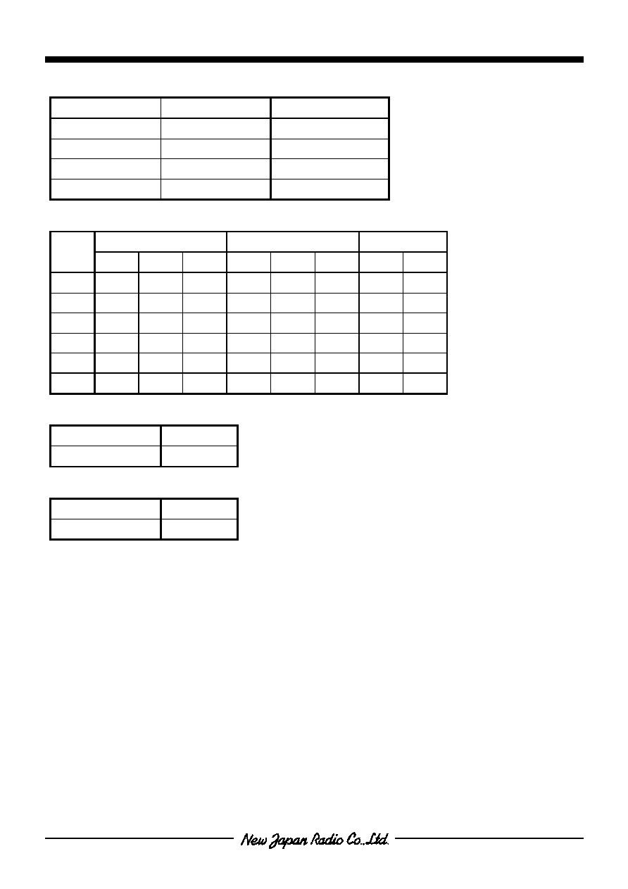
SPEED DISCRIMINATOR COUNT TABLE
N1
N2
NUMBER OF COUNTS
High or Open
High or Open
128
High or Open
Low
512
Low High
or
Open 256
Low Low 1024
s
THREE PHASE LOGIC TRUTH TABLE
F/R=L F/R=H
OUTPUTS
H 1
H 2
H 3
H 1
H 2
H 3
Source
Sink
1 H L H L H L VH
UL
2 H L L L H H
WH
UL
3 H H L L L H
WH
VL
4 L H L H L H UH
VL
5 L H H H L L UH
WL
6 L L H H H L VH
WL
s
S/S TERMINAL
High or Open
Stop
Low Start
s
BRAKE TERMINAL
High or Open
Brake
Low Release

Preliminary
NJW4302
- 12 -
s
TYPICAL APPLICATION
PVCC
VCC
VREG
DGND
AGND
VSH
CR
CROCK
R
C
FI
L
O
FI
L
I
IN
T R
E
F
TO
C
IN
T OU
T
IN
T IN
D
OU
T
PO
UT
LD
BR
F
R
WL
VH
VL
UH
UL
RF
H3
-
H3+
H2-
H2+
H1-
H1+
FGIN+
FGIN-
FGOUT
FGSOUT
PGND
AGND
N2
N1
SS
CLK
NJW4302 QFP44
WH
0.47u
2k
0.1u
1000p
100k
FGS
C
0.47u
2.4M
18k
150k
220p
0.22u
0.1u
27k
100p
20k
0.047u
1500p
VSH
75k
47u
Q
VR
R
10
R
12
R
13
R
14
C
4
R
3
R
7
C
9
R
11
R
9
C
10
R
8
C
8
R
2
C
3
C
2
C
1
R
1
C
6
C
5
C
7
R
4
R
5
R
6
C
VR
VM
Preliminary
NJW4302
- 13 -
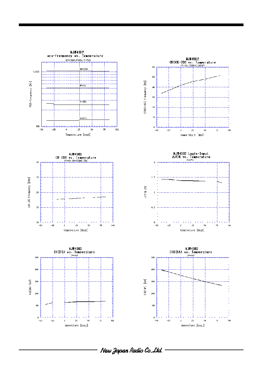
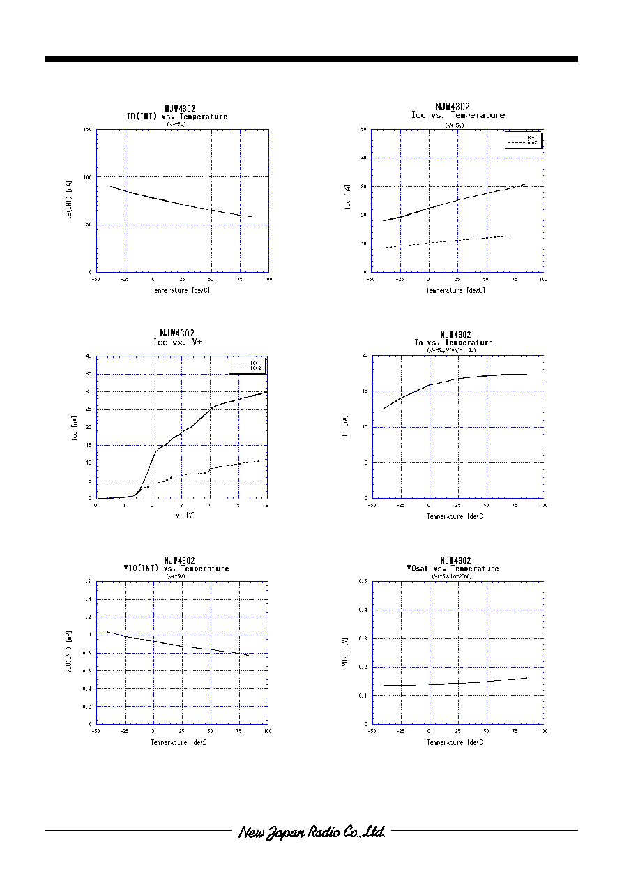
s
TYPICAL CHARACTERISTICS
Preliminary
NJW4302
- 14 -
s
TYPICAL CHARACTERISTICS
(Ta=25degC,With standard device)

Preliminary
NJW4302
- 15 -
s
APPLICATION NOTE
∑
FG Amplifier
FG Amplifier consists of input differential amplifier and output Schmitt-trigger comparator. Input amplifier is
constructed as low-pass filter with external resistors and capacitors to reduce noise. The amplifier output level
should be over 250mVp-p to adjust gain by external resistors, due to hysteresis of Schmitt-trigger comparator.
FG+ input is biased internally to the half level of Vcc. This DC bias voltage is also used to RESET the internal logic
circuit. For stable RESET operation, It a capacitor, requires a 0.1 uF capacitor connected to FG+ terminal. RESET is
enable a during 0V to 1.25V of the voltage at the FG+.
FG Sensor Amplifier Application Circuit
NJW4302
for Internal logic
FG+
FG-
FGO
FGS
100k
2k
1000p
0.47u
0.1u

Preliminary
NJW4302
- 16 -
∑
FG interfac for logic output device
The circuit below is a FG interface for logic output device (i.e. Hall IC and optical encoder). Two external
resistors are required to adjust the input voltage within the common mode input voltage range,0 to Vcc-1.5V.
∑
Power supply generating from Vref
To supply for NJM4302, Hall sensor and Power stage, QR1 should have 100mA current capacity. It needs 47
microfarad capacitor on V+ of NJW4302 for ripple filtering.
∑
Hall sensor biasing
Hall biasing is determined by Hall signal amplitude. Hall signal amplitude must be larger than input sensitivity
of NJW4302.
∑
FG Input
Internal FG Amplifier is a differential amplifier which inputs and output are pin-outed. The DC gain of this
amplifier, A
FG
, is:
8
7
R
R
A
FG
=
C8 is for noise reduction, C9 is for DC cut. Typical value of C10 is 0.1 microfarad. The inductor symbol
connected FGIN is FG sensing copper pattern on PC board.
∑
Power supply generating from Vref
To supply for NJM4302, Hall sensor and Power stage, QR1 should have 100mA current capacity. It needs 47
microfarad capacitor on V+ of NJW4302 for ripple filtering.
∑
Hall sensor biasing
Hall biasing is determined by Hall signal amplitude. Hall signal amplitude must be larger than input sensitivity
of NJW4302.
FG interface for logic level input
0.1u
NJW4302
for Internal logic
FG +
FG -
FGO
FG
1.5k
3.5k
logic
5 V

Preliminary
NJW4302
- 17 -
∑
FG Input
Internal FG Amplifier is a differential amplifier and both inputs and output are connected to the pin. The DC gain
of this amplifier, A
FG
, is:
8
7
R
R
A
FG
=
C8 is for compensation or noise reduction, C9 is for DC cut. Typical value of C10 is 0.1 microfarad. The
inductor symbol connected FGIN is FG sensing copper pattern on PC board.
∑
PWM Frequency
PWM clock generates by CR oscillator. The frequency is:
1
1
48
.
0
1
C
R
f
PWM
=
In fig.x*, f
PWM
is about 19kHz. If f
PWM
is about 20kHz, it could reduce audible noise.
∑
Variable range of VCO frequency
VCO frequency in typical value is recommend 160kHz to 1MHz. External constants is:
R2 = 20k ohm, C3 = 100pF, R3 = 27k ohm, C4 = 0.47 uF
If it can not be settled into this range, change the division of speed discriminator.
∑
Detecting time of rock protection
Detecting time is settled by C2 as follow:
2
66 C
t
ROCK
=
In fig.x*, t
rock
is about 3.1 sec.
∑
Integration Amplifier
Both speed discriminator output and PLL output should be mixed via two resistors before input to INTIN of
Integration Amplifier. Mixing resistor, Timing resistors and capacitors are necessary for good system operation.
C6 is need for non-polar type capacitor for good stability.
∑
∑
∑
∑
Upper power transistor
To reduce ripple of power line, Upper output transistor is connect NJM4302 via common-base NPN transistors.
Minimum output current is 12mA, it is able to drive 1A class transistor. If more current is needed, change the
output transistor to Darlington type. Re-circulating diodes is needed on between collector and emitter of output
transistor.
∑
Lower power transistor
Lower output could drive external power transistor directly to about 1.5A. If more current is needed, change
the output transistor to Darlington type. The resistor connected between base and emitter of power transistor is
necessary on PWM operation for sharp cut-off of power transistor. When your system have any noise, attach a
capacitor in parallel the resistor.
Re-circulating diodes is needed on between collector and emitter of output transistor. R11 is a current sensing
resistor and settled by following:
O
RE
I
V
R
=
11
When VRF is sensing voltage, Io is sensing current. Take care of power dissipation of R11, also.

Preliminary
NJW4302
- 18 -
∑
Recirculation Diodes
Recirculation diodes are recommend to use Shottkey-burrier type. Forward voltage "VF" and reverse returning
time "trr" are contributed for power dissipation.
[CAUTION]
The specifications on this databook are only
given for information , without any guarantee
as regards either mistakes or omissions. The
application circuits in this databook are
described only to show representative usages
of the product and not intended for the
guarantee or permission of any right including
the industrial rights.